Oxidation dynamics of ultrathin GaSe probed through Raman spectroscopy
Abstract
Gallium selenide (GaSe) is a 2D material with a thickness-dependent gap, strong non-linear optical coefficients and uncommon interband optical selection rules, making it interesting for optoelectronic and spintronic applications. In this work, we monitor the oxidation dynamics of GaSe with thicknesses ranging from 10 to 200 nm using Raman spectroscopy. In ambient temperature and humidity conditions, the intensity of all Raman modes and the luminescence decrease rapidly with moderate exposure to above-gap illumination. Concurrently, several oxidation products appear in the Raman spectra: Ga2Se3, Ga2O3 and amorphous and crystalline selenium. We find that no safe measurement power exists for optical measurements on ultrathin GaSe in ambient conditions. We demonstrate that the simultaneous presence of oxygen, humidity, and above-gap illumination is required to activate this photo-oxidation process, which is attributed to the transfer of photo-generated charge carriers towards aqueous oxygen at the sample surface, generating highly reactive superoxide anions that rapidly degrade the sample and quench the optical response of the material.
Gallium selenide (GaSe) is a layered pseudo-direct gap semiconductorNagel1979 with strong non-linear properties in the visible, IR and THZ ranges Allakhverdiev2009 ; Mandal2008 , a high photoresponse from 2 to 5 eV Ho2006b , a highly anisotropic band structure exhibiting uncommon selection rules Liang1975 ; Kuroda1981 , and interesting spin physics Starukhin2010 . Atomically thin GaSe can be mechanically exfoliated from bulk samples Late2012 ; Hu2012 or grown by chemical vapor transport Lei2013 . Its bulk band gap of Aulich1969a ; Allakhverdiev2009 is predicted to increase to more than for the monolayer Rybkovskiy2011 ; Hu2013 . Atomically thin flakes and devices have shown a high photoresponse Li2014d ; Hu2012 , a composition tunable band gap Jung2015 , near-unity optical polarization Tang2015 , the strongest second-harmonic generation observed in a monolayer 2D material Karvonen2015 ; Zhou2015a , and transistors with high ON/OFF ratios Late2012b .
Like most 2D materials, the properties of GaSe are expected to sensitively depend on the interaction of its surface with its chemical environment. In bulk form, GaSe is generally considered as a stable material and is known to have a high laser damage threshold suitable for non-linear optics applications Fernelius1994 ; Allakhverdiev2013 . Nonetheless, bulk GaSe is also known to naturally form a native oxide Drapak2008a and thermally- and photo-induced oxidation has been reported Katerynchuk2014 ; Iwakuro1982 ; Kovalyuk2008 . Recently, exposure to intense laser light was found to degrade optical properties and lead to chemical transformations Beechem2015 ; Andres-Penares2017 ; Susoma2017 . Given the interest for few-layer GaSe for electronic and optoelectronic applications, it appears critical to examine the oxidation dynamics of ultrathin GaSe and determine the conditions in which this oxidation can be suppressed or at least minimized.
In this paper, we monitor the complex oxidation dynamics of ultrathin GaSe and identify the emergence of several oxidation products using Raman spectroscopy. This oxidation, highly detrimental to all optical and electronic processes, requires the simultaneous presence of oxygen, humidity, and above-gap illumination and is adequately described in the framework of the Marcus-Gerischer theory. We demonstrate that removing any of these three components greatly reduces the oxidation rate.
GaSe layers were mechanically exfoliated from Bridgeman-grown bulk crystals Jandl1976 using PDMS stamps onto silicon (Si) substrates covered with a thermal oxide (SiO2). Flakes with thicknesses ranging from 10 to were identified by optical contrast using an optical microscope and their thickness was established from atomic force microscopy (AFM) measurements. Raman measurements were conducted in backscattering geometry using a single-mode laser. The spatial and spectral resolution were and , respectively. For sample in vacuum experiments, samples were exfoliated in a dry N2-flushed environment and transferred to an optical cell evacuated to a pressure of . Deoxygenated water vapor was obtained from deionized water subjected to several freeze-thaw cycles under vacuum. Experiments in oxygen were done using 99.999% O2 gas (3 ppm H2O) at a partial pressure of . Finally, measurements in ambient air were done at a temperature of and under a 48% relative humidity.
Raman spectra are used to monitor the integrity of thin GaSe layers and the appearance of photo-induced oxidation products. In this first experiment, samples were exposed to of radiation at , which corresponds to about of the established laser damage threshold for nanosecond pulses at May1997 . This illumination is about above the bandgap of GaSe. Fig. 1 presents the evolution of the Raman spectrum as a function of exposure time for a 45 nm thick GaSe sample in air. Freshly exfoliated GaSe measured in vacuum (pristine GaSe) presents the usual dominant Raman modes expected from bulk GaSe Hoff1975 ; Jandl1976 ; Wieting1972 : at , at , and at . Two other vibrational modes located at and at were often observed from pristine GaSe. These Raman modes are also associated to bulk GaSe Wieting1972 ; Hoff1975 ; Jandl1976 , but they will not be considered in this work due to their much weaker intensity compared to , and .
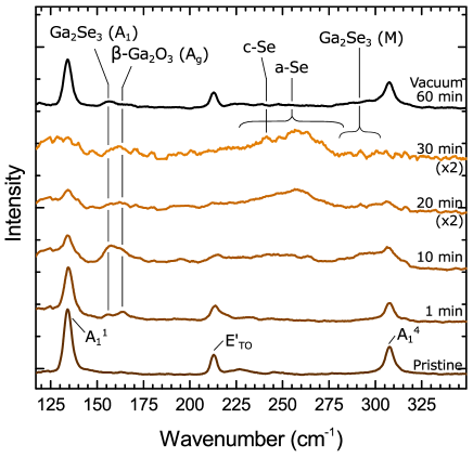
The Raman spectrum evolves significantly as a function of exposure time. The intensity of all features associated with GaSe rapidly decreases and several additional Raman modes appear at frequencies of , , and . All GaSe vibrational modes are already accounted for Hoff1975 ; Wieting1972 and none of these additional features can be related to any of the various known GaSe polytypes. They are attributed to a photo-induced chemical transformation of GaSe and corresponds to well-known thermal oxidation products: Ga2Se3 , a-Se, -Ga2O3 (see §SI in Supplementary Material for a description of the three main thermal oxidation pathways and their activation temperatures).
The frequency and width of the first mode at corresponds to the vibrational mode of Ga2Se3 Finkman1975 . Although Ga2Se3 exhibits several Raman-allowed modes, the one at is the narrowest and most intense Yamada1992 ; Markl1995 ; Finkman1975 and thus the more likely to be observed. Ga2Se3 has a defect zinc-blende structure in which Ga vacancies may or may not be ordered. The polarization-resolved Raman measurements presented in Fig. S1(a) in Supplementary Material suggest that the photo-induced -Ga2Se3 phase is polycrystalline. Another feature related to Ga2Se3 is observed at after a 10 min photoexposure. This broad () feature actually corresponds to a group of at least three vibrational modes with various symmetry representations (, , ) that have been assigned to localized vibrational modes of vacancy-disordered Ga2Se3 Yamada1992 . For its connection with multiple vibrational modes, this feature is labeled Ga2Se3 (M). Its presence suggests a high level of disorder in the Ga2Se3 phase.
After exposure of 20 min and more, the Raman signal is dominated by two even broader features. The first at likely corresponds to SeO2 or SeO3 Raman modesAnderson2000 ; Brassington1987 , but a quantitative analysis of this feature has proven difficult; it will not be further discussed. The other feature at matches the characteristics of a mode associated to selenium Balitskii2002 ; Beechem2015 and its width () suggests an amorphous phase (a-Se) Carroll1981 ; Baganich1991 . The narrower peak () at appears last and is associatedLucovsky1967 to a selenium crystalline phase (c-Se). As it has been often demonstrated, a-Se easily photo-crystallizes Poborchii1998 ; Ishida1997 .
The feature observed at does not correspond to any modes belonging to GaSe, -Ga2Se3 , or Se and its oxides. However, its frequency and width match the characteristics of the vibrational mode of -Ga2O3 Onuma2014 ; Dohy1982 . According to Ref. Dohy1982, , this feature should be the second most intense Raman feature from -Ga2O3 ; the most intense one, found in single crystals at , has not been unambiguously observed in this work. Polarization-resolved data is presented in Fig. S1(b) in the Supporting Information.
The formation of these oxidation products is monitored as a function of time through the intensity of their Raman modes. Fig. 2 (a) shows that the relative integrated intensity of all GaSe modes (, , ) rapidly decreases with time. After of exposure, relative Raman intensities have dropped to 15% of their initial values, revealing that the integrity of the GaSe layer is severely compromised by photo-induced oxidation mechanisms. The luminescence intensity measured at also rapidly decreases (see Fig. S2 in the Supplementary Material).
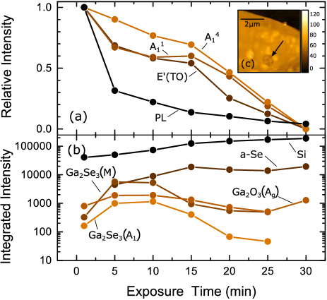
Fig. 2 (b) shows the integrated intensity of the oxidation products. After only one minute of exposure, the intensity of these modes is substantial and easily measurable. -Ga2Se3 and Ga2Se increase to a maximum value after 5- and then decrease below the detection limit after . -Ga2O3 appears and then retains a relatively constant intensity throughout the oxidation process. In contrast, the intensity of a-Se rapidly increases and eventually plateaus at an intensity significantly higher than that of all other observed Raman modes, as can be seen in Fig. 1.
Direct oxidation of GaSe into and Se has been shown to dominate at low temperatures Balitskii2004 ; Drapak2008a ; Stakhira2005 and, after complete oxidation involving high temperatures, only and elemental selenium should remain Berchenko1997 (see §SI of Supplementary Material). The rapid initial increase in intensity of all modes associated to Ga2Se3, Ga2O3 and Se suggests that more than one oxidation pathway is activated and that thermal oxidation is not the dominant mechanism due to the low temperatures involved. As detailed in §II of the supplementary material, the temperature increase occurring in the experiment presented in Figs 1 and 2 is less than .
The Raman intensity is proportional to the quantity of material in the probed volume, but it is also sensitive to its structural quality. It is therefore difficult to establish the concentrations of crystalline oxidation products, as, for example, the decrease of both Ga2Se3 modes could be related to its oxidation into Ga2O3 (see §SI of the Supplementary Material) or to the degradation of its crystalline structure as the oxidation progresses. During oxide formation, excess Se segregates at the surface Drapak2008a . As seen from Fig. 2(b), its intensity quickly increases at short exposure times and mirrors the drop of intensity of GaSe Raman modes and luminescence signal. Because its response is much less sensitive to its structural quality, -Se is believed to be the most reliable Raman marker of oxidation amongst the various products (see also §V in Supplementary Material).
The Raman signal from the Si substrate located underneath the GaSe flake steadily increases with time even though the excitation conditions are rigorously controlled. This is explained by the generation of a large-gap oxide and localized ablation. Oxidation leads to the formation of -Ga2O3 with a gap of Tippins1965 , which is transparent at the excitation energy of . Also, post-exposure AFM measurements indicate a layer-by-layer thinning induced by the laser exposure (see Fig. 2 (c)). This is explained by the high volatility of Se and the high atomic mobility of the remaining metallic Ga Markl1995 . As a net result, the absorption from the GaSe flake decreases.
As suggested by the data presented in Fig. 1 (topmost curve), placing the sample in a vacuum environment protects GaSe samples from photo-induced oxidation. Curve A presented in Fig. 3 shows the evolution of the Raman intensity of a thick flake as a function of time for an excitation power of . For such thin layers, this power yields a weak but measurable Raman signal. The intensity of GaSe Raman modes is only marginally affected after an exposure of more than in vacuum. At the time indicated by the vertical dashed line, the sample was exposed to ambient air. After a few minutes, the Raman intensity has dropped by two orders of magnitude and the signal is completely lost after . This clearly shows that thin GaSe flakes are unstable in ambient conditions and that minimal laser illumination is sufficient to induce significant degradation, establishing that no safe above-gap excitation power exists for atomically-thin samples.
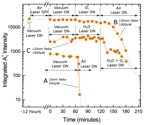
Curve B presented in Fig. 3 shows the Raman intensity of of a flake exposed to of laser intensity. For the first data point, the sample is in vacuum. The sample is then exposed to ambient air without any illumination. After 12 hours, the sample is again measured under vacuum conditions and the Raman intensity is very similar to that initially measured, indicating that exposure to oxygen and water vapor alone does not induce significant chemical changes. After of laser illumination in vacuum, no appreciable change in intensity is observed, even though residual H2O is present in the sample chamber and on the sample. Then, dry oxygen (3 ppm H2O) is introduced in the optical cell and the sample is exposed to radiation for another . A slight change in Raman intensity is observed, but the overall signal loss is minor because of the limited amount of H2O available at the sample. Finally, the sample is exposed to ambient air and continually illuminated for another . It takes about for the intensity to change significantly. This delay is attributed to a relatively slow nucleation and initial growth of degradation by-products for thicker samples. From that point on however, a rapid decline of intensity takes place, losing more than one order of magnitude within less than one hour. Curve C in Fig. 3 shows the Raman intensity from a flake measured in vacuum and then in deoxygenated water vapor. The Raman intensity does not show any appreciable change after 1 hour in each environment. Introduction of oxygen in the chamber at the 120 min mark leads to a rapid decrease in the Raman intensity. These experiments establish that continuous above-gap illumination, water vapor and oxygen alone do not support the photo-oxidation process, but that the simultaneous presence of all three is required.
Although the observed oxidation byproducts are those observed from thermally-activated oxidation (Eqs. (S1a)-(S1c) in the Supplementary Material), the photo-oxidation process observed in this work is not temperature driven. The Raman shifts observed correspond to a temperature variation of at most at the studied exposure powers (see §SII in the Supplementary Material for the detailed analysis). This result confirms that the above gap illumination is not contributing significant heat, but rather generating an carrier density in the conduction band.
The results presented thus far suggest that the photo-oxidation involves these three steps: optical excitation of carriers, electron transfer towards aqueous () oxygen molecules at the surface of the sample, and spontaneous reaction between aqueous oxygen superoxide anions (O) with the -doped semiconductor. This process can be modeled using the following equations:
| (1a) | ||||
| (1b) | ||||
| (1c) | ||||
where represents GaSe with photoexcited electron hole pairs, and represents GaSe oxidation byproducts. Although the photo-driven dynamics are expected to be quite different from the thermal dynamics discussed in Ref. Balitskii2004, , our results confirm that the oxidation byproducts are similar.
The charge transfer between the photo-excited carriers and aqueous oxygen (Eq. (1b)) can be understood in the framework of the Marcus-Gerischer theory, where the rate of charge transfer is described by Favron2015 Favron2015 :
| (2) |
where is the conduction band electron density, and are the concentrations of neutral oxygen and superoxide in the water at the sample surface, is the GaSe electron affinity, is the Fermi level of the oxygen-water solution and is the solvent reorganization energy around oxygen molecules. Since GaSe has an electron affinity which positions the lower conduction band in line with the aqueous oxygen acceptor states, the exponential function in Eq. 2 enables charge transfer towards the aqueous O2 (see §SVI in the supplementary material). The generated aqueous superoxide anions (O) at the surface then rapidly react with the p-doped GaSe (Eq. (1c)) to produce the observed oxidation byproducts, which will in turn decrease the observed GaSe Raman intensity.
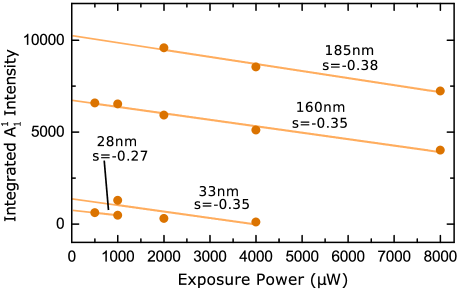
In the thickness regime studied here, the band gap variation is negligible,Rybkovskiy2011 ; Hu2013 and the absorption coefficient is independent of thickness. The rate at which superoxide anions are generated is thus proportional to the exposure power, . Fig. 4 shows the intensity of obtained after an exposure of 15 min at the indicated exposure power in ambient air for samples of varying thicknesses. As predicted by Eq. (2), the observed degradation rate increases linearly with exposure power and is independent of sample thickness, as evidenced from the very similar slopes measured. This confirms the role of the linear dependence of the photo-oxidation mechanism on above gap illumination and further rules out thermal processes.
In summary, GaSe exhibits a relatively complex oxidation dynamics compared to other 2D materials. It involves several components : oxygen, humidity, and above-gap illumination, and results in the generation of several oxidation products, Ga2Se3, Ga2O3 and amorphous and crystalline selenium. Luminescence and Raman measurements in ambient conditions are found to severely degrade the optical and electronic characteristics of GaSe, indicating that no safe illumination threshold exists, especially for thin layers of GaSe. Hence, the study of the intrinsic characteristics of 2D GaSe requires a controlled environment at all stages of processing and characterization.
See supplementary material for more detail on the thermal oxidation process and thermal effects, for further analysis of the polarized Raman spectra of the oxide products and of sample photoluminescence, and for additional information regarding the role of water vapor and oxygen in the oxidation process.
This work was made possible by funding from the Fonds de Recherche du Québec-Nature et Technologie (FRQNT) and the Natural Sciences and Engineering Research Council of Canada (NSERC).
References
- (1) S. Nagel, A. Baldereschi, and K. Maschke, Journal of Physics C: Solid State Physics 12, 1625 (1979).
- (2) K. R. Allakhverdiev, M. Ö. Yetis, S. Özbek, T. K. Baykara, and E. Y. Salaev, Laser Physics 19, 1092 (2009).
- (3) K. C. Mandal, S. H. Kang, M. Choi, J. Chen, X.-C. Zhang, J. M. Schleicher, C. A. Schmuttenmaer, and N. C. Fernelius, IEEE Journal of Selected Topics in Quantum Electronics 14, 284 (2008).
- (4) C. H. Ho, M. H. Hsieh, and C. C. Wu, Review of Scientific Instruments 77, 113102 (2006).
- (5) W. Y. Liang, Journal of Physics C: Solid State Physics 8, 1763 (1975).
- (6) N. Kuroda and Y. Nishina, Physica B+C 105, 30 (1981).
- (7) A. N. Starukhin, D. K. Nelson, and B. S. Razbirin, Journal of Experimental and Theoretical Physics 111, 645 (2010).
- (8) D. J. Late, B. Liu, H. S. S. R. Matte, C. N. R. Rao, and V. P. Dravid, Advanced Functional Materials 22, 1894 (2012).
- (9) P. Hu, Z. Wen, L. Wang, P. Tan, and K. Xiao, ACS nano 6, 5988 (2012).
- (10) S. Lei, L. Ge, Z. Liu, S. Najmaei, G. Shi, G. You, J. Lou, R. Vajtai, and P. M. Ajayan, Nano letters 13, 2777 (2013).
- (11) E. Aulich, J. L. Brebner, and E. Mooser, Physica Status Solidi (C) 31, 129 (1969).
- (12) D. V. Rybkovskiy, N. R. Arutyunyan, A. S. Orekhov, I. A. Gromchenko, I. V. Vorobiev, A. V. Osadchy, E. Y. Salaev, T. K. Baykara, K. R. Allakhverdiev, and E. D. Obraztsova, Physical Review B 84, 085314 (2011).
- (13) P. Hu, L. Wang, M. Yoon, J. Zhang, W. Feng, X. Wang, Z. Wen, J. C. Idrobo, Y. Miyamoto, D. B. Geohegan, and K. Xiao, Nano letters 13, 1649 (2013).
- (14) X. Li, M.-W. Lin, A. A. Puretzky, J. C. Idrobo, C. Ma, M. Chi, M. Yoon, C. M. Rouleau, I. I. Kravchenko, D. B. Geohegan, and K. Xiao, Scientific Reports 4, 5497 (2014).
- (15) C. S. Jung, F. Shojaei, K. Park, J. Y. Oh, H. S. Im, D. M. Jang, J. Park, and H. S. Kang, ACS Nano 9, 9585 (2015).
- (16) Y. Tang, W. Xie, K. C. Mandal, J. A. McGuire, and C. W. Lai, Journal of Applied Physics 118, 113103 (2015).
- (17) L. Karvonen, A. Säynätjoki, S. Mehravar, R. D. Rodriguez, S. Hartmann, D. R. T. Zahn, S. Honkanen, R. A. Norwood, N. Peyghambarian, K. Kieu, H. Lipsanen, and J. Riikonen, Scientific Reports 5, 10334 (2015).
- (18) X. Zhou, J. Cheng, Y. Zhou, T. Cao, H. Hong, Z. Liao, S. Wu, H. Peng, K. Liu, and D. Yu, Journal of the American Chemical Society 137, 7994 (2015).
- (19) D. J. Late, B. Liu, J. Luo, A. Yan, H. S. S. R. Matte, M. Grayson, C. N. R. Rao, and V. P. Dravid, Advanced Materials 24, 3549 (2012).
- (20) N. C. Fernelius, Prog. Crystal Growth and Charact 28, 275 (1994).
- (21) K. Allakhverdiev. In Proceedings of SPIE, T. N. Dreischuh and A. T. Daskalova, editors, volume 8770, 877003, mar (2013).
- (22) S. I. Drapak, S. V. Gavrylyuk, Z. D. Kovalyuk, and O. S. Lytvyn, Semiconductors 42, 414 (2008).
- (23) V. N. Katerynchuk, Z. R. Kudrynskyi, and Z. D. Kovalyuk, Inorganic Materials 50, 339 (2014).
- (24) H. Iwakuro, C. Tatsuyama, and S. Ichimura, Japanese Journal of Applied Physics 21, 94 (1982).
- (25) Z. Kovalyuk, V. Katerynchuk, A. Savchuk, and O. Lytvyn, Superlattices and Microstructures 44, 416 (2008).
- (26) T. E. Beechem, B. M. Kowalski, M. T. Brumbach, A. E. McDonald, C. D. Spataru, S. W. Howell, T. Ohta, J. A. Pask, and N. G. Kalugin, Applied Physics Letters 107, 173103 (2015).
- (27) D. Andres-Penares, A. Cros, J. P. Martínez-Pastor, and J. F. Sánchez-Royo, Nanotechnology 28, 175701 (2017).
- (28) J. Susoma, J. Lahtinen, M. Kim, J. Riikonen, and H. Lipsanen, AIP Advances 7, 015014 (2017).
- (29) S. Jandl, J. L. Brebner, and B. M. Powell, Physical Review B 13, 686 (1976).
- (30) M. May, S. Debrus, K. Zakrzewska, H. Benisty, and A. Chevy, Journal of the Optical Society of America B 14, 1048 (1997).
- (31) R. M. Hoff, J. C. Irwin, and R. M. A. Lieth, Canadian Journal of Physics 53, 1606 (1975).
- (32) T. J. Wieting and J. L. Verble, Physical Review B 5, 1473 (1972).
- (33) E. Finkman, J. Tauc, R. Kershaw, and A. Wold, Physical Review B 11, 3785 (1975).
- (34) A. Yamada, N. Kojima, K. Takahashi, T. Okamoto, and M. Konagai, Japanese Journal of Applied Physics 31, 186 (1992).
- (35) A. Märkl, M. von der Emde, C. Nowak, W. Richter, and D. Zahn, Surface Science 331, 631 (1995).
- (36) A. Anderson, A. Sanders, and W. Smith, Journal of Raman Spectroscopy 31, 403 (2000).
- (37) N. J. Brassington, H. G. M. Edwards, and V. Fawcett, Spectrochimica Acta Part A: Molecular Spectroscopy 43, 451–454 (1987).
- (38) O. A. Balitskii, V. P. Savchyn, and V. O. Yukhymchuk, Semiconductor Science and Technology 17, L1 (2002).
- (39) P. J. Carroll and J. S. Lannin, Solid State Communications 40, 81 (1981).
- (40) A. Baganich, V. Mikla, D. Semak, A. Sokolov, and A. Shebanin, Phys. Stat. Sol. 166, 297 (1991).
- (41) G. Lucovsky, A. Mooradian, W. Taylor, G. B. Wright, and R. C. Keezer, Solid State Communications 5, 113 (1967).
- (42) V. V. Poborchii, A. V. Kolobov, and K. Tanaka, Applied Physics Letters 72, 1167 (1998).
- (43) K. Ishida and K. Tanaka, Physical Review B 56, 206 (1997).
- (44) T. Onuma, S. Fujioka, T. Yamaguchi, Y. Itoh, M. Higashiwaki, K. Sasaki, T. Masui, and T. Honda, Journal of Crystal Growth 401, 330 (2014).
- (45) D. Dohy, G. Lucazeau, and A. Revcolevschi, Journal of Solid State Chemistry 45, 180 (1982).
- (46) O. Balitskii and V. Savchyn, Materials Science in Semiconductor Processing 7, 55 (2004).
- (47) Y. Stakhira and N. Tovstyuk, Materials Science and Engineering: B 116, 112 (2005).
- (48) N. Berchenko, O. Balitskii, R. Lutsiv, V. Savchyn, and V. Vasyltsiv, Materials Chemistry and Physics 51, 125 (1997).
- (49) H. H. Tippins, Physical Review 140, A316 (1965).
- (50) A. Favron, E. Gaufres, F. Fossard, A.-L. Phaneuf-L’Heureux, N. Y.-W. Tang, P. L. Levesque, A. Loiseau, R. Leonelli, S. Francoeur, and R. Martel, Nat Mater 14, 826 (2015).