Two-Dimensional Lattice Model for the Surface States of Topological Insulators
Abstract
The surface states in three-dimensional (3D) topological insulators can be described by a two-dimensional (2D) continuous Dirac Hamiltonian. However, there exists the Fermion doubling problem when putting the continuous 2D Dirac equation into a lattice model. In this paper, we introduce a Wilson term with a zero bare mass into the 2D lattice model to overcome the difficulty. By comparing with a 3D Hamiltonian, we show that the modified 2D lattice model can faithfully describe the low-energy electrical and transport properties of surface states of 3D topological insulators. So this 2D lattice model provides a simple and cheap way to numerically simulate the surface states of 3D topological-insulator nanostructures. Based on the 2D lattice model, we also establish the wormhole effect in a topological-insulator nanowire by a magnetic field along the wire and show the surface states being robust against disorder. The proposed 2D lattice model can be extensively applied to study the various properties and effects, such as the transport properties, Hall effect, universal conductance fluctuations, localization effect, etc.. So it paves a new way to study the surface states of the 3D topological insulators.
pacs:
73.20.-r, 71.10.Pm, 73.63.Nm, 74.62.EnI Introduction
The three-dimensional (3D) topological insulators (TIs), which possess both insulating bulk states and conducting surface states protected by time-reversal symmetry, have attracted intense attentionHMZ ; Qxl . The surface states present an odd number of gapless Dirac cones and are robust against time-reversal-invariant disorders due to their spin-momentum locked helical properties. The surface states have been confirmed by the angle-resolved photoemission spectroscopy (ARPES) experimentsHD ; Chen ; Xia . However, it is a challenge to observe quantum transport of the surface states , which are usually covered by bulk carriers caused by material defectsButchN . Recently, several unambiguous experimental observations of quantum Hall effect based on surface states have been obtained in TI materialsYXu1 ; RYoshimi ; NKoirala ; YXu2 . Another experimental evidence for the surface transport is the Aharonov-Bohm conductance oscillations in a TI nanowire with a magnetic field paralleling the wireHPeng ; FXiu ; Dufouleur ; SHong ; SCho . The oscillations are subject to an anomalous phase shift of half flux quanta arising from a Berry phase for surface states on a curved surface in 3D TI nanowiresGRosenberg ; JBardarson ; REgger ; YZhang .
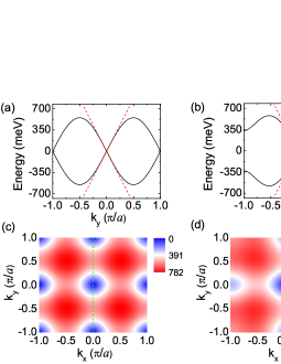
On the other hand, to quantitatively simulate the transport properties of surface states, a low-energy lattice model is desirable to describe the thin films or nanostructures of 3D TIs. The 3D TIs can be described by a continuous 3D effective model with parameters that obtained by fitting the energy spectrum from ab initio calculationsHZhang ; CXLiu ; WYShan . By discretizing the 3D effective model, a 3D cubic lattice Hamiltonian can be a candidate for further calculations. Moreover, a 3D Fu-Kane-Mele model in diamond lattice with spin-orbit interactions can also realize 3D TI phase by choosing suitable parametersLFu . However, it is computationally expensive to do calculations basing on the Hamiltonian derived from a 3D lattice model. To acquire a high-accuracy result, a huge-dimension Hilbert space is needed. Despite of insulating bulk states, the low-energy description of surface states in 3D TIs around the Dirac node is solely given by a massless 2D Dirac Hamiltonian. The 2D lattice model can greatly reduce the computational cost with a same precision in comparison with 3D lattice model. However, there exists the Fermion doubling problem, when placing the massless 2D Dirac equation into a lattice formNielsen ; Kogut ; Vafek2 . As shown in Fig.1(c), three additional Dirac nodes appear at boundaries of the first Brillouin zone. This has impeded the utility of a 2D lattice model to quantitatively study the fascinating transport properties related to surface states in 3D TIs.
In this paper, we propose a square-lattice model in terms of 2D Dirac Hamiltonian with a Wilson term to describe the surface states of 3D TIs. We show that the modified 2D lattice model can mimic the linear dispersion of surface states near the point and opens energy gaps at the spurious Dirac cones located at boundaries of the Brillouin zone (see Fig.1). In particular, its Berry phase is very close to for the low Fermi level case, which is well consistent with 3D model. The proposed 2D model can be extensively applied to study the various properties and effects of the surface states of the 3D topological insulator, such as the transport properties, Hall effect, universal conductance fluctuations, localization effect, band structures, and so on. Moreover, as an example of the application, the electrical and transport properties of a cuboid TI nanowire are studied by employing the proposed 2D lattice model. The results show that the surface spectrum opens a small gap and is doubly degenerate, which is same with the band structure calculated from 3D model. From the 2D lattice model, we also establish the wormhole effect by threading a magnetic flux across the cross section of TI nanowire. Further, we obtain a consistent picture for the conductance of a clean TI nanowire from both the 2D and 3D lattice models and show that the conductance is robust against the surface disorders. All these investigations show that the proposed 2D lattice model can faithfully describe the surface states of 3D TI in the long wavelength limit. Note that the numerical calculation based on the 2D lattice model is much quicker than the one based on 3D model.
The rest of the paper is organized as follows. In Sec. II, the theoretical model and the methods for describing the surface states of 3D TI are presented. In Sec. III, we demonstrate the utility of the proposed 2D lattice model by studying the band structure and transport properties of a cuboid TI nanowire. Sec. IV discusses the advantages of the proposed 2D lattice model. Finally, a brief summary is given in Sec. V.
II Model and Methods
The low-energy 2D effective Hamiltonian for the surface states of 3D TI isLHZ ; LiuH ,
| (1) |
where is the Fermi velocity, with the Pauli matrices, is the momentum, and is the normal vector of a specific surface. Its spectrum has a single Dirac cone construction with , in which is the component of perpendicular to . For simplicity, we take parallel to z direction and in the following. Now, we discretize the Hamiltonian in Eq.(1) to obtain a square lattice Hamiltonianbook1 ,
| (2) |
where and are the annihilation and creation operators at site , respectively. () is the primitive vectors of quare lattice along the x (y) direction, and is the lattice constant. In this paper, we set the Fermi velocity and the lattice constant . This Fermi velocity corresponds to topological insulator and , which can be experimentally extracted from ARPES and scanning tunneling spectroscopy.RYoshimi ; ZhangT
It can be seen from the band structure shown in Fig.1(a) that the lattice Hamiltonian can reproduce the linear spectrum of the effective Hamiltonian in Eq.(1) near the point. Unfortunately, the lattice model also has low-energy excitations with linear dispersion in the vicinity of points (0,). We can identify four Dirac cones in the first Brillouin zone [see Fig. 1(c)]. As mentioned above, this is the Fermi doubling problem in a lattice model for chiral Weyl fermions and involved with continuous chiral symmetryNielsen . In order to avoid the Fermi doubling problem, we introduce a Wilson term with a zero bare mass into the lattice HamiltonianKogut ; Vafek2 :
| (3) |
which is the counterpart of a continuous term . In fact, the Wilson term which includes the Pauli matrix acts as a momentum-dependent mass term and breaks the chiral symmetry explicitly. For momentum near the point, i.e., the center of Brillouin zone, the Wilson term vanishes quadratically, and thus the spectrum keeps gapless, in the long wavelength limit. However, for the doubler fermions, that are the states at boundaries of the first Brillouin zone, the Wilson term is nonvanishing and opens a finite gap. One also can obtain the same conclusion from the spectrum of the lattice Hamiltonian. The spectrum of Hamiltonian in a lattice can be formulated by . For , approaches to , which gives a linear dispersion at the low energy case. The Wilson term can open an energy gap at points (0,) and (,0) [Fig.1(b)] and a gap at points , so that three additional Dirac cones arising from the Fermi doubling are removed, leaving the single one near the point [Fig.1(d)]. On the other hand, if the Fermi level is low (small Fermi momentum ), the Berry phase for eigenstates of Hamiltonian around the Fermi surface is modulo , which is very closed to the Berry phase of surface states in 3D TIs, although the Wilson term has broken the time-reversal symmetry. Therefore, the lattice Hamiltonian can restore properties of surface states in the long wavelength limit.

III Band structure and transport properties
Next, we quantitatively study the properties of a cuboid TI nanowire [see Fig.3(a)] based on the lattice Hamiltonian proposed above. The nanowire has a cross section of a size and is invariant under translation along the y axis, so that the momentum is a good quantum number. To study the surface states of 3D TI nanostructure with non-planar surfaces, one has to solve the Dirac Hamiltonian in curved 2D spacesLeeD1 ; VafekO . For a cuboid TI nanowire, one can completely describe the surface states by different Hamiltonians on specified surfaces as provided in Eq. (1) supplemented with matching conditions at boundary linesBreyL ; Deb . Furthermore, by some local unitary transformations, an effective 2D model can be derived for the four surfacesTM ; TM2 ; ZhouY . For the -x/-z/+x surfaces, we make rotations by fixing the y axis and the original x axis is changed into z/-x/-z axes. After corresponding unitary transformations, the effective 2D Hamiltonian for surface states reads
| (4) |
with
where and are the annihilation and creation operators at site respectively. N is the total number of lattices encircle the TI nonowire.
To demonstrate the effectiveness of this 2D lattice Hamiltonian, we firstly calculate the band structure of surface states for a 3D TI nanowire [see Fig.2]. Without the Wilson term (), each band is fourfold degenerate and the low-energy spectrum emerges at both and as shown in Fig.2(a). Two of the quadruplet can be ascribed to the redundant species doubling at boundary with in the first Brillouin zone [see Fig.1(c)]. These band structures, even if at the low energy, are completely different with 3D TI models in Eq.(1) or Eq.(5). However, by introducing the Wilson term with , it can be clearly observed in Fig.2(b) that the redundant degenerate modes are shifted away from the doubly degenerate ones. Now each band is twofold degenerate due to the same eigenvalues for surface states on the opposite surface. A large gap is opened at and the low-energy spectrum only involves in the vicinity of point. Here a small gap is also opened at because of the Berry phase for carriers taking a circle around the nanowire.
Here, it is worth noting that the coefficient in the Wilson term needs to be fine tuned in the calculation. For the smaller , the band structure of the Hamiltonian can perfectly be coincident with that of the 3D model , but the gap due to the Wilson term at the boundary of first Brillouin zone may be too small to settle the Fermion doubling problem. On the other hand, the bigger can well settle the Fermion doubling problem, but it may caused a serious departure near the point. So can not be too big and too small. While in the range of to , the band structures of the Hamiltonian can perfectly be coincident with that of from about to , and the gap is large enough at the boundary of first Brillouin zone also. This means that our method can work well in a large range of .
To further ensure the accuracy of the 2D lattice Hamiltonian in Eq.(III), we make a comparison with the low-energy approach of Zhang et al. HZhang , in which the Hamiltonian near the point has the form:
| (5) |
with , , and . are Pauli matrices in orbital space and / denote the identity matrix. In this paper, we have made further simplification that , , , and . Here the parameters and are assigned to the same values with ,HZhang and the Fermi velocity is the same with Fig. 1. These parameters guarantee the Hamiltonian with isotropy and particle-hole symmetry. By discretizing the Hamiltonian (5), we obtain a cubic lattice model by which surface states can be derived with open boundary conditionsHJiang . Fig.3(b) plots the band structure calculated from both the 2D and 3D lattice models. The two different lattice models provide very unanimous results for the spectrum in bulk gap at low energy. So the 2D lattice model proposed above is very effective for quantitative studies of the surface properties of 3D TI.
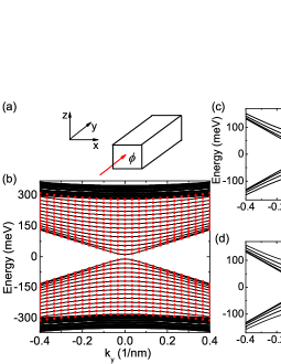
Now, we show the wormhole effect based on the 2D lattice model of Eq.(III). Since the spin-momentum locked properties of surface states, surface electron obtains a Berry phase while it goes around the four facets of a TI nonowireGRosenberg ; JBardarson ; REgger ; YZhang . The extra Berry phase yields a gapped spectrum of surface state in a TI nanowire as shown in Fig.3(c). By threading a magnetic flux along the nanowire [see Fig.3(a)], surface electron also get an Aharonov-Bohm phaseAronovA . Here, the effect of longitudinal magnetic field is included by adding a phase term to in Eq.(III), where is the vector potential for a magnetic field parallel to the y direction. By a flux , the Aharonov-Bohm phase exactly cancels the Berry phase and a pair of non-degenerate linear modes emerge with closing the gap [Fig.3(d)]. The phenomenon is known as wormhole effectGRosenberg .
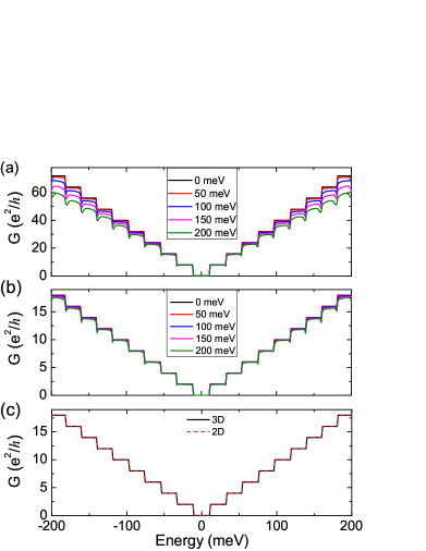
Next, we study the effectiveness of the 2D lattice Hamiltonian on the simulation of transport properties. Here, we construct a two-terminal device by dividing an infinite TI nanowire into a center region with a length and two semi-infinite left/right leads. The conductance can be calculated from the Landauer-Büttiker formula, .book1 Here the transmission coefficient , in which the , the Green function , with the Fermi energy, and being the Hamiltonian of center regionsun1 . The retarded self-energy stems from coupling to the left/right leadLeeD2 . With the presence of disorders, on each site the term in Eq.(III) is changed to , where is uniformly distributed in the range with disorder strength . Here, we only consider surface disorders in the center region. Fig.4(a) and (b) show the conductance as a function of Fermi energy at different disorder strength without and with the Wilson term, respectively. For , the conductance exhibits quantum plateaus and the results obtained from a 2D lattice model with a Wilson term agree well with the ones from a 3D lattice model while the Fermi energy is inside the bulk gap [see Fig.4(b) and (c)]. However, without the Wilson term, the 2D lattice model gives a quadrupled conductance owing to additional transport modes from Fermi doubling [Fig.4(a)]. Moreover, for , the disorders can induce scattering between the quadrupled Dirac cones and the plateau structure is distinctly destroyed for disorder strength [see Fig.4(a)]. As the Wilson term has eliminated the redundant Dirac cones, the quantum plateaus of conductance are robust against disorder [see Fig.4(b)], which is reasonable for surface state in 3D TIs. Considering that the 2D lattice model proposed in this paper has discarded bulk states, it can be used to simulate the low-energy transport properties of surface states in 3D TI systems with a large size or high accuracy in a much less expensive way.
IV Advantages of the 2D lattice model
In this section, we will discuss the advantages of the proposed 2D lattice model comparing with other methods and some potential applications. The 2D lattice model is a simplification of 3D model. In principle, it can not predict phenomena beyond the 3D model. However, in the practical calculations, the 2D lattice model can greatly improve computation speed and reduce the memory usage. This means that our method can deal systems with large size beyond the ability of 3D model and new physics may appear with increasing the size of samples. So it is more efficient than other methods in the literatures for numerical simulation. What’s more, the proposed 2D lattice model can be extensively utilized to study the various properties and effects of the surface states of the 3D topological insulator. For example, by using this 2D lattice model, one can study the transport properties, Hall effect, universal conductance fluctuations, localization effect, band structures, and so on.
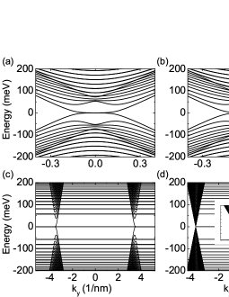
Next, we calculate the band structure in 3D TI samples under a perpendicular magnetic field to illuminate the fast computing speed and less memory usage. For a cuboid TI nanowire [see Fig.3(a)] with a cross section [here being the number of lattice along the and direction and the corresponding cross section of size ], the band structure calculated from both 3D lattice model in Eq.(5) and 2D lattice model in Eq.(4) are shown in Fig.5(a) and (b). The two models provide very coincident picture for band structure and the zero Landau level appears as expected. It is worth noting that only basis orbits are needed to obtain such results with the 2D lattice model. However, it requires basis orbits to work with the 3D lattice model. So, the new method is more efficient and much quicker. The ratio of the computation speeds based on the 2D model and 3D model is about .
Moreover, we consider another two large nanowires with a cross section and [see Fig.5(c) and (d)], both of which are described with 6392 basis orbits in the 2D lattice model. The Fig.5(c) clearly shows many unambiguous Landau levels with high index due to the large size along the direction. Moreover, as shown in Fig.5(d), a great many of nonchiral edge modes coexist with chiral edge mode in the side surface due to the large size in the direction, which can destroy the integer quantized Hall plateaus. These physics are hidden in small size samples because of the quantum confinement. Notice that it is extremely difficult for 3D lattice model to deal with such large samples. If by using the 3D lattice model, the basis orbits are and for the samples in Fig.5(c) and (d), and the computation time required are increased by about and times, respectively. So, it is impossible to obtain the results of Fig.5(c) and (d) from the 3D model. Therefore, in practical numerical simulation, the proposed 2D model can give new physics beyond 3D model.
It is also worth mention that although the conductances in Fig.4(c) from the 3D model in Eq.(5) and 2D model in Eq.(4) are very consistent, the time used in these two calculations is very different, the difference is about ten thousand times. While in the presence of the disorder, we can study the effect of the disorder on the conductances by using the 2D lattice model [see Fig.4(b)], but it is very difficult to study this effect based on the 3D model.
Based on the growth of high-quality sampleYXu1 ; RYoshimi ; NKoirala ; YXu2 , it becomes a central topic in the study of topological states that how to construct novel topological devices by utilizing the special surface states of 3D TIs. Our method can provide a cheap and accurate numerical simulations in these complicated structures, combined with the nonequilibrium Green’s function formalism, Landauer-Büttiker formula, etc. So the proposed method paves a new way to study the various properties of the surface states of the 3D TIs.
V Conclusions
In summary, we formulate a 2D lattice model for surface states of 3D TIs by appending a Wilson term with a zero bare mass to the massless Dirac equation. The Wilson term can effectively “solve” the Fermi doubling problem by opening moderate gaps at the doubled Dirac cones and maintaining the one at point. The 2D lattice model provides a very coincident picture for both low-energy band structure and conductance of a TI nanowire with respect to a 3D model, but the numerical calculations based on 2D lattice model is much quicker than based on the 3D one. Moreover, the wormhole effect can be set up in a TI nanowire under a longitudinal magnetic field. We also find that the surface states of a TI nanowire are robust against disorder.
Acknowledgments
Acknowledgments: This work was supported by NBRP of China (2015CB921102, 2014CB920901), NSF of China (11574007, 11274364, 11534001) and NSF of Jiangsu Province, China (BK20160007).
References
- (1) M.Z. Hasan and C.L. Kane, Rev. Mod. Phys. 82, 3045 (2010).
- (2) X.-L. Qi and S.-C. Zhang, Rev. Mod. Phys. 83, 1057 (2011).
- (3) D. Hsieh, Y. Xia, L. Wray, D. Qian, A. Pal, J.H. Dil, J. Osterwalder, F. Meier, G. Bihlmayer, C.L. Kane, Y.S. Hor, R.J. Cava and M.Z. Hasan, Science 323, 919(2009).
- (4) Y.L. Chen, J.G. Analytis, J.-H. Chu, Z.K. Liu, S.-K. Mo, X.L. Qi, H.J. Zhang, D.H. Lu, X. Dai, Z. Fang, S.C. Zhang, I.R. Fisher, Z. Hussain, Z.-X. Shen, Science 325, 178 (2009).
- (5) Y. Xia, D. Qian, D. Hsieh, L. Wray, A. Pal, H. Lin, A. Bansil, D. Grauer, Y.S. Hor, R.J. Cava, and M.Z. Hasan, Nat. Phys. 5, 398 (2009).
- (6) N.P. Butch, K. Kirshenbaum, P. Syers, A.B. Sushkov, G.S. Jenkins, H.D. Drew, and J. Paglione, Phys. Lett. B 81, 241301(R) (2010).
- (7) Y. Xu, I. Miotkowski, C. Liu, J. Tian, H. Nam, N. Alidoust, J. Hu, C.-K. Shih, M.Z. Hasan, and Y.P. Chen, Nat. Phys. 10, 956 (2014).
- (8) R. Yoshimi, A. Tsukazaki, Y. Kozuka, J. Falson, K.S. Takahashi, J.G. Checkelsky, N. Nagaosa, M. Kawasaki, and Y. Tokura, Nat. Commun. 6, 6627 (2015).
- (9) N. Koirala, M. Brahlek, M. Salehi, L. Wu, J. Dai, J. Waugh, T. Nummy, M.-G. Han, J. Moon, Y. Zhu, D. Dessau, W. Wu, N.P. Armitage, and S. Oh, Nano Lett. 15, 8245 (2015).
- (10) Y. Xu, I. Miotkowski, and Y.P. Chen, Nat. Commun. 7, 11434 (2016)
- (11) H. Peng, K. Lai, D. Kong, S. Meister, Y. Chen, X.-L. Qi, S.-C. Zhang, Z.-X. Shen, and Y. Cui, Nat. Mater. 9, 225 (2010)
- (12) F. Xiu, L. He, Y. Wang, L. Cheng, L.-T. Chang, M. Lang, G. Huang, X. Kou, Y. Zhou, X. Jiang, Z. Chen, J. Zou, A. Shailos, and K.L. Wang, Nat. Nanotechnol. 6, 216 (2011)
- (13) J. Dufouleur, L. Veyrat, A. Teichgräber, S. Neuhaus, C. Nowka, S. Hampel, J. Cayssol, J. Schumann, B. Eichler, O.G. Schmidt, B. Büchner, and R. Giraud, Phys. Rev. Lett. 110, 186806 (2013).
- (14) S.S. Hong, Y. Zhang, J.J. Cha, X.-L. Qi, and Y. Cui, Nano Lett. 14, 2815 (2014).
- (15) S. Cho, B. Dellabetta, R. Zhong, J. Schneeloch, T. Liu, G. Gu, M.J. Gilbert, and N. Mason, Nat. Commun. 6, 7634 (2015)
- (16) G. Rosenberg, H.-M. Guo, and M. Franz, Phys. Rev. B 82, 041104(R) (2010).
- (17) J.H. Bardarson, P.W. Brouwer, and J.E. Moore, Phys. Rev. Lett. 105, 156803 (2010).
- (18) R. Egger, A. Zazunov, and A.L. Yeyati, Phys. Rev. Lett. 105, 136403 (2010).
- (19) Y. Zhang and A. Vishwanath, Phys. Rev. Lett. 105, 206601 (2010).
- (20) H. Zhang, C.-X. Liu, X.-L. Qi, X. Dai, Z. Fang, and S.-C. Zhang, Nat. Phys. 5, 438 (2009).
- (21) C.-X. Liu, X.-L. Qi, H.J. Zhang, X. Dai, Z. Fang, and S.-C. Zhang, Phys. Rev. B 82, 045122 (2010).
- (22) W.-Y. Shan, H.-Z. Lu and S.-Q. Shen, New J. Phys. 12, 043048 (2010).
- (23) L. Fu, C.L. Kane, and E.J. Mele, Phys. Rev. Lett. 98, 106803 (2007).
- (24) H.B. Nielsen and M. Ninomiya, Nucl. Phys. B 185, 20 (1981); Phys. Lett. B 105, 219 (1981).
- (25) J.B. Kogut, Rev. Mod. Phys. 55, 775 (1983).
- (26) O. Vafek and A. Vishwanath, Annu. Rev. Condens. Matter Phys. 5, 83(2014).
- (27) H.-Z. Lu, W.-Y. Shan, W. Yao, Q. Niu, and S.-Q. Shen, Phys. Rev. B 81, 115407 (2010).
- (28) H. Liu, H. Jiang, Q.-F. Sun, and X.C. Xie, Phys. Rev. Lett. 113, 046805 (2014).
- (29) S. Datta, electronic transport in mesoscopic system, (Cambridge, 1995).
- (30) T. Zhang, P. Cheng, X. Chen, J.-F. Jia, X. Ma, K. He, L. Wang, H. Zhang, X. Dai, Z. Fang, X. Xie, and Q.-K. Xue, Phys. Rev. Lett. 103, 266803 (2009).
- (31) D.-H. Lee, Phys. Rev. Lett. 103, 196804 (2009).
- (32) O. Vafek, Phys. Rev. B 84, 245417 (2011).
- (33) L. Brey and H.A. Fertig, Phys. Rev. B 89, 085305 (2014).
- (34) O. Deb, A. Soori and D. Sen, J. Phys. Condens. Matter 26, 315009 (2014).
- (35) T. Morimoto, A. Furusaki, and N. Nagaosa, Phys. Rev. Lett. 114, 146803 (2015).
- (36) T. Morimoto, A. Furusaki, and N. Nagaosa, Phys. Rev. B 92, 085113 (2015).
- (37) Y.-F. Zhou, A.-M. Guo, and Q.-F. Sun, Phys. Rev. B 94, 085307 (2016).
- (38) H. Jiang, Z. H. Qiao, H. W. Liu, and Q. Niu, Phys. Rev. B 85, 045445 (2012).
- (39) A. G. Aronov and Y. V. Sharvin, Rev. Mod. Phys. 59, 755 (1987).
- (40) W. Long, Q.-F. Sun, and J. Wang, Phys. Rev. Lett. 101, 166806 (2008).
- (41) D.H. Lee and J.D. Joannopoulos, Phys. Rev. B 23, 4997 (1981); M.P. Lopez Sancho et al., J. Phys. F 14, 1205 (1984); 15, 851 (1985).