Low-loss Plasmonic Dielectric Nanoresonators
Abstract
Material losses in metals are a central bottleneck in plasmonics for many applications. Here we propose and theoretically demonstrate that metal losses can be successfully mitigated with dielectric particles on metallic films, giving rise to hybrid dielectric–metal resonances. In the far field, they yield strong and efficient scattering, beyond even the theoretical limits of all-metal and all-dielectric structures. In the near field, they offer high-Purcell-factor (), high-quantum-efficiency (), and highly directional emission at visible and infrared wavelengths. Their quality factors can be readily tailored from plasmonic-like () to dielectric-like (), with wide control over the individual resonant coupling to photon, plasmon, and dissipative channels. Compared with conventional plasmonic nanostructures, such resonances show robustness against detrimental nonlocal effects and provide higher field enhancement at extreme nanoscopic sizes and spacings. These hybrid resonances equip plasmonics with high efficiency, which has been the predominant goal since the field’s inception.
The material composition of an optical nanoresonator dictates sharply contrasting properties: metallic nanoparticles novotny2011antennas ; giannini2011plasmonic ; biagioni2012nanoantennas ; tsakmakidis2016large support highly subwavelength plasmons with large field strengths, but which suffer from intrinsic material losses PhysRevLett.97.206806 ; PhysRevLett.110.183901 ; PhysRevLett.112.123903 ; miller2016fundamental ; miller2015shape , whereas dielectric nanoparticles krasnok2012all ; kuznetsov_optically_2016 ; jahani2016all support exquisite low-loss versatility, but only moderate confinement as their sizes must generally be wavelength-scale or larger. In this Article, we propose and theoretically demonstrate that a combined approach—dielectric nanoparticles on metallic films—can exhibit a unique combination of strong fields and high confinement alongside small dissipative losses. We show the utility of such hybrid plasmonic dielectric resonators for (i) far-field excitations, where subwavelength silicon-on-silver nanoparticles can scatter more efficiently than is even theoretically possible for any all-metal or all-dielectric approach, and (ii) near-field excitations, where highly directional spontaneous emission enhancements are possible with quantum efficiencies and even approaching unity. Moreover, the dielectric composition of the nanoparticle, when placed atop a metallic supporting film, should mitigate much of the quantum- and surface-induced nonlocal damping that occurs at nanometer scales, an effect we confirm quantitatively with a hydrodynamic susceptibility model. Furthermore, as our approach does not rely on nanostructured metallic components, it strongly constrains parasitic dissipation arising from fabrication imperfections. More broadly, simple geometrical variations provide wide control over the individual resonant-coupling rates to photon, plasmon, and dissipative degrees of freedom, opening a pathway to low-loss, high-efficiency plasmonics.
Mitigating loss is a pivotal goal khurgin2015deal ; tassin2012comparison ; boltasseva2011low ; naik2013alternative in plasmonics. When nanoparticles interact with plane waves, their cross-sections are typically dominated by dissipative absorption. In the near field, large spontaneous-emission enhancements (Purcell factors) have been demonstrated rogobete2007design ; kinkhabwala2009large ; akselrod2014probing ; eggleston2015optical through mode-volume squeezing, but it has been typically accompanied by sub-50% quantum efficiencies at visible frequencies. Hybrid structures devilez2010compact ; rusak2014hybrid with separated dielectric (director) and metal (feed) functionality have been proposed for better radiative efficiency, but with lower enhancements. This tradeoff gives the appearance that strong and efficient plasmonic antennas are only possible at infrared frequencies khurgin2015deal , where they behave akin to perfect conductors and “plasmonic” effects are minor. Quantum corrections in plasmonics feibelman1982surface ; zhu2016quantum ; christensen2016quantum , e.g. due to electron tunneling savage2012revealing and nonlocality garcia2008nonlocal , further limit the ultimate enhancement of plasmonic resonators.
The difficulty of achieving low-loss plasmons has led to the perception that high confinement is simply incompatible with low loss, as large fields near/in a metal surface may necessarily generate significant dissipation. This intuition has led to the burgeoning field of alternative plasmonic materials boltasseva2011low ; naik2013alternative , whereby highly doped semiconductors or polar dielectrics ideally exhibit negative real permittivities with small imaginary (lossy) parts. There has been a complementary effort in all-dielectric nanoparticles krasnok2012all ; kuznetsov_optically_2016 and metamaterials kuznetsov_optically_2016 ; jahani2016all , but subwavelength resonances fundamentally require metallic components with negative permittivities khurgin2015deal ; PhysRevLett.97.206806 . Material engineering has also been proposed in the form of band engineering khurgin2010search and gain offsets zayats2013active . The perceived confinement–loss tradeoff is rigorously correct for quasistatic plasmonic resonators PhysRevLett.97.206806 , in which the desired resonant frequency directly sets the fraction of the field intensity that must reside within the lossy metal PhysRevLett.97.206806 ; PhysRevLett.110.183901 ; khurgin2012reflecting . In closed non-radiative plasmonic systems, proper geometrical optimization of dielectric-metal waveguides can reduce propagation losses oulton2008hybrid ; in open systems, the central unanswered question is whether their radiative coupling rates can be strongly increased such that radiation significantly exceeds near-field dissipative losses. Here we show that open resonators comprising high-index, low-loss nanoparticles on metallic films can simultaneously achieve high confinement and high radiative efficiencies, without significant dissipative loss.
I Conceptual Basis
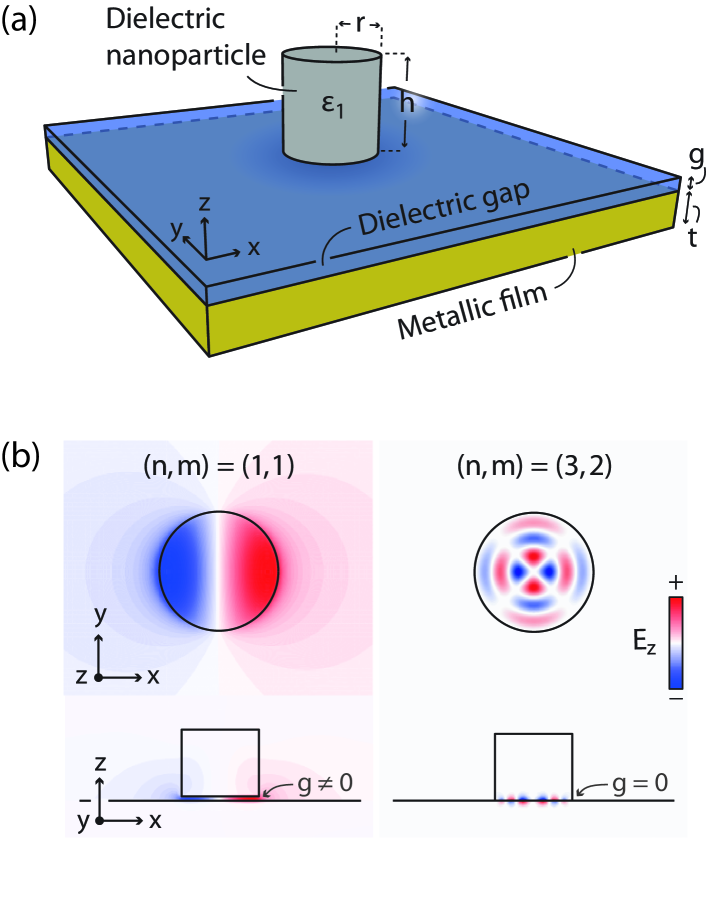
We propose a hybrid dielectric–metal resonator [Fig. 1(a)] that mitigates restrictions from metal losses on plasmonic scattering, emission, and quality factors to a great extent. The cylindrical symmetry implies that resonances can be labeled with indices , enumerating field variations in the radial and azimuthal directions, respectively. Unlike the widely used all-metal “gap-plasmon” resonances tsakmakidis2016large ; akselrod2014probing (hereafter, metal–metal resonances), which require a nonzero gap to squeeze the field inside, the dielectric–metal resonances strongly confine the resonant field for either zero or nonzero gap [Fig. 1(b)].
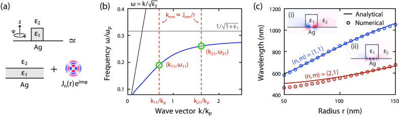
Conceptually, the dielectric–metal resonances can be understood as the surface plasmons of a planar multilayer metal–dielectric system restricted to specific quantized wavevectors . The nanoparticle’s boundary reflects surface plasmons of general wavevector without phase shift. For a cylinder of radius , the round-trip phase over the nanoparticle is given by the Bessel function of the first kind . Localized resonances are supported when this round trip phase vanishes, i.e., at the Bessel zeros :
| (1) |
Resonant frequencies are obtained by sampling the multilayer surface plasmon dispersion curve, , at the resonant wavevectors [Fig. 2(b)], as verified by the agreement between analytics and numerics [Fig. 2(c)]. Eq. (1) is most accurate for low-order resonances, when the plasmon reflection phase gordon2006light at the nanoparticle boundary is small (). Eq. (1) is also generalizable to other nanoparticle geometries and more complex multilayers.
This simple, yet accurate picture of the hybrid resonances, as part-plasmon, part-Bessel resonances, illustrates the separation of key functionality: the plasmonic metal provides vertical confinement, while the dielectric provides horizontal confinement and dictates the resonant condition. External radiative coupling occurs at the low-loss dielectric–air interface, away from the lossy metal, enabling higher radiative efficiencies than those in conventional plasmonic nanostructures.
II Far-Field Scattering
Metallic nanoparticles generally scatter more strongly than all-dielectric nanoparticles. Yet this large scattering strength—as measured, e.g., by the optical cross-section per unit particle volume—is typically accompanied by significant absorption. Thus for many applications where absorption is undesirable (such as photovoltaics atwater2010plasmonics ), the critical figure of merit is scattering strength accompanied by high radiative efficiency. Here we leverage recently developed optical-response bounds to show that low-loss dielectric nanoparticles on metallic films can achieve subwavelength scattering with large radiative efficiency, surpassing all-metal and all-dielectric scatterers and approaching fundamental limits.
There has been significant interest in finding general upper bounds to optical response gustafsson2007physical ; hugonin2015fundamental , and recently we developed new such bounds PhysRevLett.112.123903 ; miller2016fundamental ; miller2015shape . Passivity, which requires non-negative absorbed and scattered powers, imposes limits to the currents that can be excited in an absorptive scatterer, leading to bounds that are independent of shape, which account for material loss (, for material susceptibility ), and which can incorporate radiative-efficiency constraints. The bounds demonstrate miller2016fundamental that high radiative efficiency, defined as (where , , and are the scattering, absorption, and extinction cross sections, respectively), necessarily reduces the largest cross-section per volume that can be achieved. A natural figure of merit () emerges: (equivalently, ), which rewards high scattering cross-section () as well as high radiative efficiency (). The is subject to the bound miller2016fundamental
| (2) |
which depends only on the frequency , the material composition, and the incident field properties. is the ratio of the incident-field intensity (including e.g., reflection from a planar film in the absence of the nanoparticle) integrated over particle volume to the intensity of the plane wave. Perfect radiative efficiency () is unachievable for lossy scatterers, such that Eq. (2) cannot diverge. Equation (2) clearly shows that low-loss materials offer the possibility for strong and high-efficiency scattering, but all-dielectric structures cannot reach their bounds (in most parameter regimes) for lack of subwavelength resonances. On the other hand, by equipping dielectric nanoparticles with a subwavelength resonant mechanism, achieved by coupling to a metallic substrate, these high limits may actually be approached.
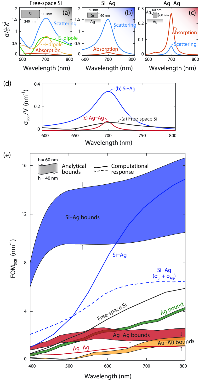
We compare scattering by three types of resonators—(i) a free-space, all-dielectric resonator, (ii) a hybrid dielectric-on-metal resonator, and (iii) a metal-on-metal resonator—at wavelength. For each resonator, the dielectric is Si. The free-space dielectric resonator [Fig. 3(a)] is designed to achieve super-scattering PhysRevLett.105.013901 (Supplementary II), with , via aligned electric- and magnetic-dipole moments. The hybrid silicon-on-silver resonator [Fig. 3(b)] is optimized to have a similar scattering cross-section, which is achieved in roughly one-fifth of the volume and with . Finally, the radius of the Ag-on-Ag resonator [Fig. 3(c)] is optimized by radius [cylinder height and gap size same as Fig. 3(b) for constant ]; notably, it only achieves only radiative efficiency. Figure 3(d) compares the scattering strengths of the three architectures, measured by , clearly showing the dielectric–metal structure’s advantage, which remains compelling across visible frequencies [Fig. 3(e)]. Fig. 3(e) compares of different structures and includes corresponding bounds (shaded regions) based on the cylinder height (Supplementary III) due to the oscillatory incident fields in the presence of the reflective film. Different from Fig. 3(a-d), all cross-sections in Fig. 3(e) (except the dashed line) isolate the contributions of the nanoparticles themselves (Supplementary IV), and the substrate is incorporated in the incident-field definition miller2015shape . At longer wavelengths, the scattering strength of the Si cylinder (blue solid line) approaches its bound, the highest among all bounds. By replacing the cylinder with a horizontally-aligned nanorod in the dielectric–metal system, scattering bounds can be saturated across the entire visible spectrum (Supplementary Fig. S1). Including film absorption and scattering in the dielectric-metal structure (blue dashed line), the hybrid resonance retains large , still outperforming all-metal and all-dielectric resonators. In the following section, we translate this large-response, high-radiative-efficiency capability from the far field to the near field.
III Near-Field Emission Enhancements
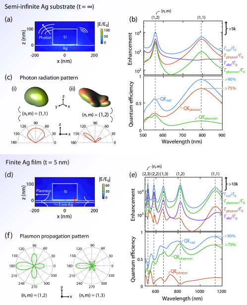
Plasmonic losses are particularly acute in the near field, for sources in close proximity to the resonator, as the source readily accesses lossy channels that dissipate energy before it can escape into a propagating far-field photon or guided plasmon. In contrast, with negligible local dissipation, dielectric–metal resonances can provide high-Purcell, high-efficiency, and high-directionality spontaneous emission enhancements. A Purcell factor with quantum efficiency (including both photon and plasmon emission) can be achieved in the optical regime. Whereas some previous work (e.g., Ref. akselrod2014probing ) has not distinguished between emission into guided plasmons and emission into radiating photons, we separate each contribution and show that a simple geometrical reconfiguration (increasing/reducing the metal-film thickness) can swing the emission rate from plasmon-dominant () to photon-dominant () or vice versa. Directional photon and plasmon emission can also be realized via high-order resonances.
We first demonstrate photon emission enhancement with a silicon cylinder on a semi-infinite Ag substrate, separated by a gap [Fig. 4(a)]. Planar dispersion analysis (Supplementary Fig. S2) suggests that this geometry should provide similar Purcell enhancement, and much higher quantum efficiency, as compared to a -gap-size metal–metal structure. We decompose yang2016near the enhanced emission from a -oriented dipole into far-field photon, guided plasmon, and local dissipative channels and obtain corresponding efficiencies (Supplementary VII) [Fig. 4(b)]. The and modes achieve Purcell factors (total enhancement) and , respectively. As importantly, the mode exhibits quantum efficiency and photon efficiency. Similar efficiencies are achieved for emitters located throughout the gap region (not shown; adopting the approach in yang2016optically ). In the far field [Fig. 4(c)], the mode exhibits wide-angle emission, while the mode enables highly directional photon emission, without the Yagi-Uda configuration devilez2010compact ; curto2010unidirectional or a periodic lattice lozano2013plasmonics .
Even higher quantum efficiencies, with similar enhancements, are possible with alternative low-loss dielectric materials (on Ag). AlSb zollner1989dielectric nanoparticles offer close-to-unity efficiencies below their direct bandgap. Ge nanoparticles exhibit Purcell factors of with high radiative () and photon () efficiencies at the technologically relevant wavelength (Supplementary Fig. S3). Relative to a previously proposed rogobete2007design infrared antenna with similar efficiency, this Purcell factor is 10 times higher.
We further demonstrate plasmon generation gan2012proposal with high efficiency by using an optically thin () metal layer [Fig. 4(d)]. The thin metal improves the modal overlap between the gap and propagating plasmons yang2016optically . The Purcell factors exceed 104 for all the modes in Fig. 4(e). Similar to the thick-metal case, high total quantum efficiencies are achieved, with that of the mode still 90%. Contrary to the thick-metal case, photon emission is suppressed while plasmon emission is strongly boosted: the plasmon efficiency exceeds 60% for each of the , and modes. The guided-plasmon propagation pattern [Fig. 4(f)] reveals highly directional plasmon launching.
IV Widely Varying Quality Factors
The quasistatic properties of metals PhysRevLett.97.206806 limit the quality factors of conventional plasmonic resonances (typically 100 in the optical regime), imposing severe restrictions on many plasmonic applications. In contrast, dielectric–metal resonances provide control over the individual absorptive- and radiative-loss rates, providing options along the entire continuum between the all-metal and all-dielectric extremes.
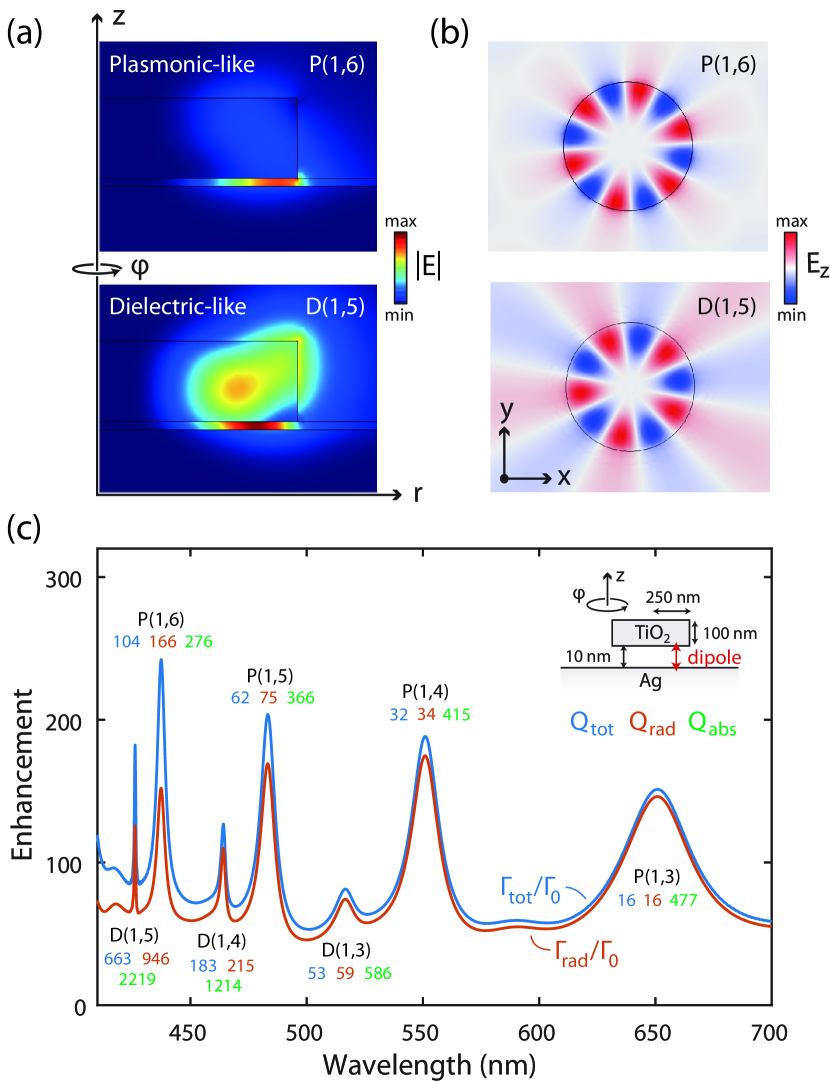
Using approximately lossless dielectrics, such as TiO2 at visible frequencies, plasmonic modes with extraordinarily high quality factors can be designed (Fig. 5). As evidenced by their field patterns [Fig. 5(a–b)], the modes of the dielectric–metal resonator partition into dielectric-like and plasmonic-like resonances—both of which display strong field confinement within the gap. Figure 5(c) shows the total, radiative, and absorptive quality factors (, , and ) of the resonances (Supplementary VIII). The dielectric-like modes generally have higher than the plasmonic-like modes because of their larger field intensity in the interior of the dielectric [Fig. 5(a)]. Unlike conventional plasmonic modes, for which is mainly limited by material loss, here is primarily limited by radiation loss, which can be readily tailored via the nanoparticle geometry and size. The of these resonances ranges widely from to , offering a wide, continuous design space for narrow- or broad-band plasmonic applications.
V Robustness to Plasmonic Quantum Corrections
Quantum phenomena beyond the classical description set the ultimate limitations on the achievable response in plasmonic nanostructures. Chief among these phenomena are nonlocality, spill-out, and surface-enabled damping feibelman1982surface . In Ag, their joint impacts are well-described by a nonlocal, effective model—GNOR mortensen2014generalized (Supplementary IX), a convective-diffusive hydrodynamic model—causing spectral blueshifting and broadening in structures with nanoscale features. In comparison, analogous quantum corrections in dielectrics are negligible due to the absence of free carriers. We show here that the dielectric–metal resonances display increased robustness to these detrimental quantum corrections compared to their metal–metal counterparts; taking field enhancement as a measure, the former is even superior for gaps .
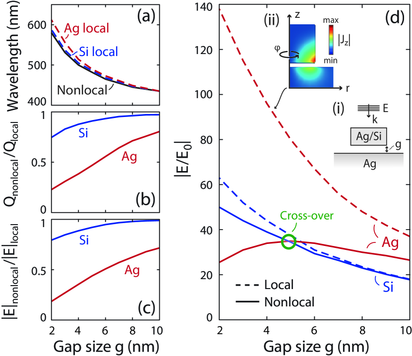
Figure 6 examines these quantum corrections for gap sizes, where inter-surface electron tunneling is absent zhu2016quantum . For both dielectric–metal and metal–metal structures (with equal nonlocal resonant frequencies), the resonant wavelength, quality factor, and field enhancement of the resonance are shown [Fig. 6(a-c)] as functions of gap size. Relative to local, classical predictions, both configurations exhibit blueshifted resonant wavelengths and reductions in quality factor and field enhancement—all of which increase as the gap size decreases. Crucially, the metal–metal system suffers more severe reductions than its counterpart. This observation can be attributed to two cooperating effects: first, in light of the plasmon–Bessel framework laid out above (Fig. 2), the planar multilayer equivalent approximately dictates the gap-dependent impact of quantum corrections. Accordingly, since the surface plasmon of the planar metal–dielectric–metal system suffers increased impact of quantum corrections compared to the planar dielectric–metal system (by a factor christensen2016quantum and see Supplementary Fig. S5), the metal–metal nanoparticle’s performance is similarly reduced. Second, the metal nanoparticle’s edges host sharply varying current densities [Fig. 6(d), inset (ii)] and consequently incur large nonlocal corrections in these regions.
Strikingly, the relative robustness of the hybrid resonances to quantum corrections enables them to demonstrate larger absolute field enhancements, for equal gap sizes [Fig. 6(d)], than the high-intensity, pure-plasmonic metal–metal resonators. The enhancement in the latter system deteriorates drastically at these gap sizes, due to the above-noted distinguishing aspects. The comparative robustness of the hybrid resonances suggests a pathway to stronger light–matter interactions in extreme nanoscale gaps chikkaraddy2016single .
VI Discussion
In this Article, we have shown the possibility for low-loss plasmonics by coupling low-loss dielectric nanoparticles with high-confinement metallic substrates. The hybrid dielectric–metal resonances exhibit strong and efficient scattering and near-field emission enhancements, large quality factors, and nonlocal robustness beyond those of conventional plasmonic nanostructures.
By avoiding any structured metallic components, the architecture has practical fabrication advantages. Single- or poly-crystalline metallic films exhibit much lower losses wu2014intrinsic ; mcpeak2015plasmonic than metallic nanoparticles (which are typically amorphous, with more severe surface roughness). Moreover, this approach avoids the use of any metallic corners or tips that may strongly absorb due to fabrication imperfections.
The approach to high efficiency presented here can work in tandem with future material improvements. Just as we have shown that re-architecting common materials can improve their plasmonic response, new, low-loss materials should be integrated into these hybrid geometries rather than conventional all-metal structures. Graphene sheets behave optically very much like ultrathin metallic films, and thus our approach extends to dielectric-on-graphene architectures for efficient graphene plasmon confinement.
Looking forward, the dielectric-metal approach prompts two directions for new exploration. First, the strong emission enhancement of the dielectric–metal resonances rely on the high index contrast between the dielectric scatterer and the dielectric spacer (comprising the gap). When the index contrast is reduced, the high efficiencies can be maintained though at the expense of reduced optical confinement. Thus continued development of very-low-index () materials, such as low-index SiO2 xi2007optical , aerogels sun2008enhanced , and low-index polymers groh1991lowest , would further increase enhancements and improve efficiencies. Second, quantum effects in dielectric and dielectric–metal structures at few-nanometer length scales are of increasing interest, and should be explored further with alternative (e.g., time-dependent density functional theory) electronic and optical models. The prospect of dielectric–metal structures that are robust to deleterious nonlocal effects is especially enticing for the growing field of quantum plasmonics fitzgerald2016quantum .
Methods
Methods and any associated references are available in the Supplementary Information.
Acknowledgements
The authors thank fruitful discussions with Prof. Koppens and Dr. Bo Zhen. This work was partly supported by the Army Research Office through the Institute for Soldier Nanotechnologies under contract No. W911NF-13-D-0001. Y.Y. was partly supported by the MRSEC Program of the National Science Foundation under Grant No. DMR-1419807. O.D.M. was supported by the Air Force Office of Scientific Research under award number FA9550-17-1-0093. T.C. was supported by the Danish Council for Independent Research (Grant No. DFF C6108-00667). M.S. was partly supported (reading and analysis of the manuscript) by S3TEC, an Energy Frontier Research Center funded by the U.S. Department of Energy under grant no. DE-SC0001299.
Author contributions
M.S. conceived the project. Y.Y., O.D.M., and T.C. developed the analytical models and theoretical analysis. J.D.J. and M.S. supervised the project. All authors contributed to discussions and manuscript writing.
Additional Information
Correspondence and requests for materials should be addressed to Y.Y. and O.D.M.
Competing financial interests
The authors declare no competing financial interests.
References
- (1) Novotny, L. & Van Hulst, N. Antennas for light. Nat. Photonics 5, 83–90 (2011).
- (2) Giannini, V., Fernández-Domínguez, A. I., Heck, S. C. & Maier, S. A. Plasmonic nanoantennas: fundamentals and their use in controlling the radiative properties of nanoemitters. Chem. Rev. 111, 3888–3912 (2011).
- (3) Biagioni, P., Huang, J.-S. & Hecht, B. Nanoantennas for visible and infrared radiation. Rep. Prog. Phys. 75, 024402 (2012).
- (4) Tsakmakidis, K. L., Boyd, R. W., Yablonovitch, E. & Zhang, X. Large spontaneous-emission enhancements in metallic nanostructures: towards leds faster than lasers. Opt. Express 24, 17916–17927 (2016).
- (5) Wang, F. & Shen, Y. R. General properties of local plasmons in metal nanostructures. Phys. Rev. Lett. 97, 206806 (2006).
- (6) Raman, A., Shin, W. & Fan, S. Upper bound on the modal material loss rate in plasmonic and metamaterial systems. Phys. Rev. Lett. 110, 183901 (2013).
- (7) Miller, O. D. et al. Fundamental limits to extinction by metallic nanoparticles. Phys. Rev. Lett. 112, 123903 (2014).
- (8) Miller, O. D. et al. Fundamental limits to optical response in absorptive systems. Opt. Express 24, 3329–3364 (2016).
- (9) Miller, O. D., Johnson, S. G. & Rodriguez, A. W. Shape-independent limits to near-field radiative heat transfer. Phys. Rev. Lett. 115, 204302 (2015).
- (10) Krasnok, A. E., Miroshnichenko, A. E., Belov, P. A. & Kivshar, Y. S. All-dielectric optical nanoantennas. Opt. Express 20, 20599–20604 (2012).
- (11) Kuznetsov, A. I., Miroshnichenko, A. E., Brongersma, M. L., Kivshar, Y. S. & Luk yanchuk, B. Optically resonant dielectric nanostructures. Science 354, aag2472 (2016).
- (12) Jahani, S. & Jacob, Z. All-dielectric metamaterials. Nature nanotechnology 11, 23–36 (2016).
- (13) Khurgin, J. B. How to deal with the loss in plasmonics and metamaterials. Nat. Nanotechnol. 10, 2–6 (2015).
- (14) Tassin, P., Koschny, T., Kafesaki, M. & Soukoulis, C. M. A comparison of graphene, superconductors and metals as conductors for metamaterials and plasmonics. Nat. Photon. 6, 259–264 (2012).
- (15) Boltasseva, A. & Atwater, H. A. Low-loss plasmonic metamaterials. Science 331, 290–291 (2011).
- (16) Naik, G. V., Shalaev, V. M. & Boltasseva, A. Alternative plasmonic materials: beyond gold and silver. Adv. Mater. 25, 3264–3294 (2013).
- (17) Rogobete, L., Kaminski, F., Agio, M. & Sandoghdar, V. Design of plasmonic nanoantennae for enhancing spontaneous emission. Opt. Lett. 32, 1623–1625 (2007).
- (18) Kinkhabwala, A. et al. Large single-molecule fluorescence enhancements produced by a bowtie nanoantenna. Nat. Photon. 3, 654–657 (2009).
- (19) Akselrod, G. M. et al. Probing the mechanisms of large purcell enhancement in plasmonic nanoantennas. Nat. Photon. 8, 835–840 (2014).
- (20) Eggleston, M. S., Messer, K., Zhang, L., Yablonovitch, E. & Wu, M. C. Optical antenna enhanced spontaneous emission. Proc. Natl. Acad. Sci. 112, 1704–1709 (2015).
- (21) Devilez, A., Stout, B. & Bonod, N. Compact metallo-dielectric optical antenna for ultra directional and enhanced radiative emission. ACS Nano 4, 3390–3396 (2010).
- (22) Rusak, E. et al. Hybrid nanoantennas for directional emission enhancement. Appl. Phys. Lett. 105, 221109 (2014).
- (23) Feibelman, P. J. Surface electromagnetic fields. Prog. Surf. Sci. 12, 287–407 (1982).
- (24) Zhu, W. et al. Quantum mechanical effects in plasmonic structures with subnanometre gaps. Nat. Commun. 7 (2016).
- (25) Christensen, T., Yan, W., Jauho, A.-P., Soljačić, M. & Mortensen, N. A. Quantum corrections in nanoplasmonics: shape, scale, and material. arXiv preprint arXiv:1608.05421 (2016).
- (26) Savage, K. J. et al. Revealing the quantum regime in tunnelling plasmonics. Nature 491, 574–577 (2012).
- (27) García de Abajo, F. J. Nonlocal effects in the plasmons of strongly interacting nanoparticles, dimers, and waveguides. J. Phys. Chem. C 112, 17983–17987 (2008).
- (28) Khurgin, J. B. & Sun, G. In search of the elusive lossless metal. Appl. Phys. Lett. 96, 181102 (2010).
- (29) Zayats, A. V. & Maier, S. A. Active plasmonics and tuneable plasmonic metamaterials (Wiley Online Library, 2013).
- (30) Khurgin, J. B. & Boltasseva, A. Reflecting upon the losses in plasmonics and metamaterials. MRS Bull. 37, 768–779 (2012).
- (31) Oulton, R. F., Sorger, V. J., Genov, D., Pile, D. & Zhang, X. A hybrid plasmonic waveguide for subwavelength confinement and long-range propagation. Nat. Photon. 2, 496–500 (2008).
- (32) Gordon, R. Light in a subwavelength slit in a metal: propagation and reflection. Phys. Rev. B 73, 153405 (2006).
- (33) Atwater, H. A. & Polman, A. Plasmonics for improved photovoltaic devices. Nat. Mater. 9, 205–213 (2010).
- (34) Gustafsson, M., Sohl, C. & Kristensson, G. Physical limitations on antennas of arbitrary shape. In Proc. R. Soc. A, vol. 463, 2589–2607 (The Royal Society, 2007).
- (35) Hugonin, J.-P., Besbes, M. & Ben-Abdallah, P. Fundamental limits for light absorption and scattering induced by cooperative electromagnetic interactions. Phys. Rev. B 91, 180202 (2015).
- (36) Ruan, Z. & Fan, S. Superscattering of light from subwavelength nanostructures. Phys. Rev. Lett. 105, 013901 (2010).
- (37) Yang, J., Hugonin, J.-P. & Lalanne, P. Near-to-far field transformations for radiative and guided waves. ACS Photon. 3, 395–402 (2016).
- (38) Yang, Y. et al. Optically thin metallic films for high-radiative-efficiency plasmonics. Nano Lett. 16, 4110–4117 (2016).
- (39) Curto, A. G. et al. Unidirectional emission of a quantum dot coupled to a nanoantenna. Science 329, 930–933 (2010).
- (40) Lozano, G. et al. Plasmonics for solid-state lighting: enhanced excitation and directional emission of highly efficient light sources. Light: Sci. Appl. 2, e66 (2013).
- (41) Zollner, S., Lin, C., Schönherr, E., Böhringer, A. & Cardona, M. The dielectric function of AlSb from 1.4 to 5.8 ev determined by spectroscopic ellipsometry. J. Appl. Phys. 66, 383–387 (1989).
- (42) Gan, C. H., Hugonin, J.-P. & Lalanne, P. Proposal for compact solid-state III-V single-plasmon sources. Phys. Rev. X 2, 021008 (2012).
- (43) Mortensen, N. A., Raza, S., Wubs, M., Søndergaard, T. & Bozhevolnyi, S. I. A generalized non-local optical response theory for plasmonic nanostructures. Nat. Commun. 5 (2014).
- (44) Chikkaraddy, R. et al. Single-molecule strong coupling at room temperature in plasmonic nanocavities. Nature 535, 127–130 (2016).
- (45) Wu, Y. et al. Intrinsic optical properties and enhanced plasmonic response of epitaxial silver. Adv. Mater. 26, 6106–6110 (2014).
- (46) McPeak, K. M. et al. Plasmonic films can easily be better: rules and recipes. ACS Photon. 2, 326–333 (2015).
- (47) Xi, J.-Q. et al. Optical thin-film materials with low refractive index for broadband elimination of fresnel reflection. Nat. Photon. 1, 176–179 (2007).
- (48) Sun, Y. & Forrest, S. R. Enhanced light out-coupling of organic light-emitting devices using embedded low-index grids. Nat. Photon. 2, 483–487 (2008).
- (49) Groh, W. & Zimmermann, A. What is the lowest refractive index of an organic polymer? Macromolecules 24, 6660–6663 (1991).
- (50) Fitzgerald, J. M., Narang, P., Craster, R. V., Maier, S. A. & Giannini, V. Quantum plasmonics. Proc. IEEE PP, 1–16 (2016).