Giant magnetoresistance and anomalous transport in phosphorene-based multilayers with noncollinear magnetization
Abstract
We theoretically investigate the unusual features of the magnetotransport in a monolayer phosphorene ferromagnetic/normal/ferromagnetic (F/N/F) hybrid structure. We find that the charge conductance can feature a minimum at parallel (P) configuration and a maximum near the antiparallel (AP) configuration of magnetization in the F/N/F structure with -doped F and -doped N regions and also a finite conductance in the AP configuration with the N region of -type doping. In particular, the proposed structure exhibits giant magnetoresistance, which can be tuned to unity. This perfect switching is found to show strong robustness with respect to increasing the contact length and tuning the chemical potential of the N region with a gate voltage. We also explore the oscillatory behavior of the charge conductance or magnetoresistance in terms of the size of the N region. We further demonstrate the penetration of the spin-transfer torque into the right F region and show that, unlike graphene structure, the spin-transfer torque is very sensitive to the chemical potential of the N region as well as the exchange field of the F region.
pacs:
73.63.-b, 75.70.Cn, 85.75.-d, 73.43.QtI Introduction
Recently, a new type of material consisting of a black phosphorus monolayer (phosphorene) has emerged as a viable candidate in the field of two-dimensional (2D) materials Li14 ; Liu14 ; andre . Unlike graphene which has a planar structure, phosphorene forms a puckered honeycomb structure, owing to an hybridization with a high in-plane structure anisotropy which has been affected in the optical and transport properties of phosphorene Liu15 ; Das14 ; Kamalakar15 ; Lu14 ; Fei14 ; Wang1 . Charge-carrier mobilities are very high at room temperature cm2 V-1 S-1 Li14 and they exhibit a strongly anisotropic behavior in phosphorene-based field effect transistor with a high on/off ratio of Liu14 . The band structure of few-layer black phosphorus has a direct gap, spanning a wide range in the visible spectrum from to eV Du10 ; Tran14 ; cakir14 ; Liang14 ; Rodin14 . The edge magnetism has been explored in different edge cutting directions Zhu14 ; Du15 ; Yang16 ; Farooq15 ; Farooq16 . The introduction of transition-metal atoms induces magnetism, where the magnitude of the magnetic moment depends on the metal species and the result can be tuned by the applied strain Hu15 ; Sui15 ; Seixas15 . Also, it is found that a spin-polarized state appears in monolayer black phosphorus by nonmagnetic impurity doping khan15 . These properties make phosphorene a quite interesting 2D material for next-generation electronic and spintronic devices based on the spin degree of freedom, which are almost dissipationless unlike those based on the charge degree of freedom fabian .
The conservation of angular momenta between itinerant electrons and localized magnetization in magnetic materials leads to the fascinating concept of spin-transfer torque; the spin angular momentum of the electrons can be transferred to the magnetization via their mutual exchange coupling which enables us to derive the dynamics of magnetization by charge current. Sloncwezski and Berger were the first to theorize about the existence of this phenomenon Berger ; Slonczewski . It is found to be important in all known magnetic materials and present in a variety of material structures and device geometries composed of magnetic-nonmagnetic multilayers such as magnetic tunnel junctions, spin valves, point contacts, nanopillars, and nanowires Brataas . The spin current flowing into the magnetic region exerts a torque on the magnetization, if the current polarization direction is non-collinear to the local magnetization in the magnetic material. This spin-transfer torque effect can cause magnetization switching for sufficiently large currents without the need for an external field. The switching aspect provides a unique opportunity to create fast-switching spin-transfer torque magnetic random access memories (STT-MRAM) Parkin , with the advantage of low power consumption and better scalability over conventional MRAMs which use magnetic fields to flip the magnetization. The spin-torque oscillator is another prominent example that serves as a field generator for microwave-assisted recording of hard-disk drives Zhu08 . Also, the spin-transfer torque leads to the spin-torque diode effect in magnetic tunnel junctions Tulapurkar . Therefore, this new discovery in condensed matter and material physics has expanded the means available to manipulate the magnetization of magnetic materials and as a result has accelerated technological development of high-performance and high density magnetic storage devices fabian ; Fert ; Brataas ; Bauer ; linder15 . Another important quantity in this field is the tunneling magnetoresistance which occurs at ferromagnetic/normal/ferromagnetic (F/N/F) hybrid structures. The resistance of the junction is different for parallel (P) and anti-parallel (AP) magnetiozation configurations and it can be experimentally measured exp1 ; exp2 . Spin-polarized resonant tunneling has been intensely studied Glazov ; Zheng ; Ertler because of its potential for applications in spin-transfer torque switching enhancement Chatterji , cavity polaritons using the resonant tunneling diode Nguyen , and in the spin-dependent resonant tunneling devices for tuning the tunneling magnetoresistance Yuasa ; Petukhov .
In the present work, we investigate the charge and spin transport characteristics of the monolayer phosphorene F/N/F hybrid structure in which the two F regions with noncollinear magnetization are connected through the normal segment of length . We model our system within the scattering matrix formalism datta . A similar study has been utilized in graphene fnfgraphene1 ; fnfgraphene2 and silicene fnfsilicene . Within the scattering formalism, we find that the transmission probability of an incoming electron from the spin band of the left F region of the F/N/F structure with P configuration of magnetization has a decreasing behavior with respect to an increase of the incidence angle, while a peak structure appears for an incoming -band electron in the proposed structure with small length . We demonstrate the appearance of a peak structure with perfect transmission for the -band electron together with additional peaks in the transmission probability of the -band electron, by increasing the contact length . However, both the incoming electrons from the and bands to the F/N/F structure with AP alignment of magnetization vectors have decreased transmission probabilities with the increase of the angle of incidence for small contact lengths and peak structures for large contact lengths.
The application of a local gate voltage to the large-length N region of the F/N/F structure leads to the amplification of transmission probability at defined angles of incidence and the attenuation of the transmission at other traveling modes in the proposed structure with the -doped N region. The - or -type doping is the process of enhancing the magnitude of the Fermi energy in the conduction or valence band of the material, tuning the electron or hole charge carriers. Then, we evaluate how it is possible to control the magnitude of the charge conductance by means of a local gate voltage in the N region, and manipulating the magnetization directions of two F regions. Depending on the chemical potential of the F region , the charge conductance can be suppressed away from the AP alignment of magnetization and finite at AP alignment in the n-type doped F/N/F structure. In particular, it displays a maximum near the AP configuration and a minimum at the P configuration in the corresponding structure with p-doped N region. We further demonstrate that the proposed spin valve structure exhibits a remarkably large magnetoresistance in analogy to the giant magnetoresistance in magnetic materials exp1 , which can be tuned to unity for determined ranges of . More importantly, we find that the perfect spin valve effect is preserved for large lengths of the N region and shows strong robustness with respect to increasing the chemical potential with the local gate voltage. In addition, we compute the equilibrium magnetic torque exerted on the magnetic order parameter of the right F region along the and directions and demonstrate the penetration of the torque into the F region. We show that the sign change of the torque can be realized by means of the gate voltage in the N region and tuning the exchange field of the F region, in addition to its magnitude changes.
This paper is organized as follows. In Sec. II, we introduce the model and establish the theoretical framework which is used to calculate the transmission probabilities, charge conductance, spin-current density, and the spin-transfer torque. In Sec. III, we present and describe our numerical results for the proposed phosphorene-based F/N/F structure. Finally, our conclusions are summarized in Sec. IV.
II Model and basic equations
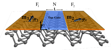
Let us consider a wide monolayer phosphorene F/N/F hybrid structure in the plane, where the N region of length couples two F regions with the magnetization vectors and , as sketched in Fig. 1. The interface between the N and F regions are located at and . It is assumed that the ferromagnetism can be induced by means of the proximity effect when it is placed with a magnetic insulator. Such an F region in graphene can be produced by using an insulating ferromagnetic substrate, or by adding F metals or magnetic impurities on top of the graphene sheet Tombros07 ; Haugen ; Swartz12 ; Wang15 ; Dugaev06 ; Uchoa08 ; Yazyev10 . The direction of the magnetization vector can be controlled by externally applied magnetic field.
The system is translationally invariant along the direction and thus the y-component of the wave vector does not change and is conserved. The effective low-energy Hamiltonian of a quasiparticle in a monolayer phosphorene, in the presence of a magnetization vector in the F region, has the form
| (1) |
which acts on a four-component spinor . The indices respectively label the conduction and valence bands, and , () denote the two spin subbands. The two sets of Pauli matrices, and , act on the real spin and the conduction and valence band pseudospin degrees of freedom, correspondingly, and is the chemical potential of the F region. The two-dimensional model Hamiltonian in the subspace of the conduction and valence bands can be described by
| (2) |
where the energies of the conduction and valence band edges, eV and eV, and the coefficients , , , in units of eV nm2, and in units of eV nm, are obtained from the first-principles simulations based on the density-functional theory (DFT) Zare ; asgari .
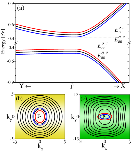
Figure 2(a) shows the anisotropic band energy dispersion of the monolayer phosphorene along the direction in the Brillouin zone, where the zero-point energy is shifted to the middle of the band gap. The isofrequency contour surface in the space of the - (-) doped monolayer phosphorene demonstrates the elliptic shape of the Fermi surfaces especially at low charge densities, as seen in Figs. 2(b) and 2(c). The black lines correspond to the N phosphorene, while the red (blue) line corresponds to the () band of the F phosphorene.
Since it is not easy to control the angle of incident charge carriers, we usually compute the conductance by integrating over the possible angles of incidence. To evaluate the charge conductance of the proposed structure at zero temperature, we use the Landauer formula landauer
| (3) |
where () describes the transmission probability of an incoming electron from the band of the left F region with an energy to the band of the right F region, is the quantum of the conductance, and .
We calculate the transmission amplitudes of the incoming -band electron and , by matching the wave functions of the three regions of the left F, N region, and the right F region (signed by 1, 2, and 3 respectively) at the two interfaces. The total wave functions in the three regions are as follows:
| (4) | |||||
| (5) | |||||
| (6) |
where,
| (7) |
and
| (8) |
| (9) |
They are, respectively, the solutions of Eq. (1) for incoming and outgoing electrons of the region with and the N region (with ) at given energies and , and transverse wave vector , with the energy-momentum relation
Here, is the chemical potential of the N() region, , , , denotes the conduction (valence) band, and () refer to the two spin subbands, and indicates the angle of propagation of the electron. Also, the two propagation directions along the axis are denoted by in . Note again that in the N region.
The propagating electron in the N(Fi) region with the velocity
| (11) |
has the longitudinal wave vector , with , , , , and . The other parameters in Eqs. (7), (8), and (9) are defined by
Finally, from the obtained expressions of the transmission amplitudes and (see the Appendix), we define the spin-current density as Stiles
| (13) |
where , and the superscript denotes the direction of the spin Pauli matrices. From now on, since we consider only incoming and outgoing quasiparticles from the conduction bands of the F region, we thus simplify using . The components of the spin-current density are obtained as follows:
| (15) | |||||
| (16) | |||||
It is worthwhile mentioning that the anisotropic feature of the band structure appears in the aforementioned equations. Finally, having calculated the above-found expressions of , we can compute the component of the spin-transfer torque, exerted on the magnetization vector of the right F region, using the following formula,
| (17) |
The resulting spin-transfer torque and also the charge conductance of the F/N/F junction will be discussed in the next section.
III Numerical results and discussions
In this section, we present our numerical results obtained using the numerical transmission amplitudes, and Eqs. (3), (13), and (17). All of the energies , , and are in units of eV. We scale the length of the N region , in units of the lattice constant in the (armchair) direction Å. Note that the chemical potential is considered the same for the both F regions.
III.1 Transmission probability
.
First, we evaluate the transmission probability of the electron from the () band of the left F region propagating with the energy equal to the chemical potential to the () band of the right F region in the proposed F/N/F structure with different alignments of magnetization vectors. Due to the translational invariance along the direction, the -component of the wave vector is conserved. Therefore, there will be critical angles of incidence for different transmission processes above which certain types of transmissions are forbidden.
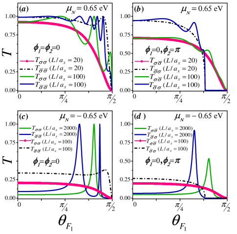
Figure 3 presents the behavior of the transmission probabilities in terms of the angle of incidence for the parallel (P) and antiparallel (AP) configuration of magnetization, respectively, in the left and right panels. We set the chemical potential of the -type F and -(-)type doped N regions eV and eV, respectively, and the exchange field eV. Since the exchange field is finite, the strength of the barrier potential is different for incoming electrons from different spin subbands [see Fig. 2(a)]. In the P configuration, the transmission probability () is less than the and monotonically decreases with for a small length of the N region (), while a peak structure with unit transmission appears for [see Fig. 3(a)]. Increasing the value leads to the appearance of a peak structure for together with additional peaks with unit amplitudes for . The unity is attained in prerequisite condition when , where is an integer value Zheng . In the AP configuration, the transmission probabilities of both the and band electrons have decreasing behavior with , and peak structures with appear with the increase of the contact length [see Fig. 3(b)]. Note that there is a critical angle of incidence defined as for the incoming electron from the band above which the corresponding wave becomes evanescent and does not contribute to any transport of charge. We find (not show) that decreasing the value of the exchange field leads to the enhancement of the transmission probabilities and , and appearance of the peak structure with perfect transmissions. We mention that the transmission probabilities between different spin subbands (, ) in the P configuration and also between equal spin subbands (, ) in the AP configuration are equal to zero.
Furthermore, the effect of a local gate voltage in the N region of the proposed structure on the transmission probabilities is shown in the bottom panel of Fig. 3 for the P [Fig. 3(c)] and AP [Fig. 3(d)] configurations. It is seen that increasing the value leads to the perfect transmission, where is satisfied, at defined angles of incidence and attenuation of the transmission at other traveling modes, in the corresponding structure with -doped N region.
III.2 Charge conductance
.
.
Now, we proceed to investigate the charge conductance of the proposed F/N/F structure at zero temperature. We consider two cases for the chemical potential of the F region: and (see Fig. 2). The energies and define the conduction-band edges for the two spin-subbands of the F region. The incoming quasiparticles from the left F region with the chemical potential in the range are completely dominated by the electrons from the band with and while for the case of , the incoming electrons are from both and bands with and .
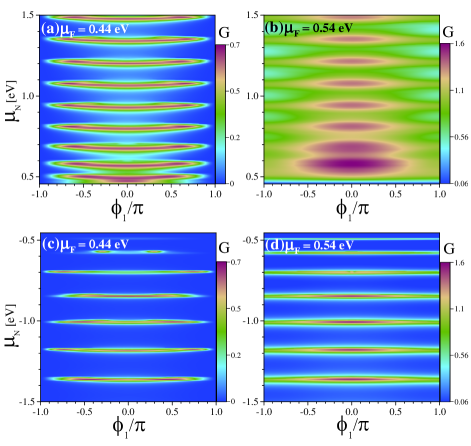
The behavior of the charge conductance of the -doped F/N/F structure (in units of ) versus the chemical potential of the N region, , and the magnetization direction of the left F region, , are demonstrated in Figs. 4(a) and 4(b) for eV () and eV (), when the magnetization direction of the right F region, , is fixed to , and . As seen, the charge conductance is an even function of and oscillates by varying with the gate voltage. The oscillations can be understood in the context of the Fabry-Prot oscillations Born . Interestingly, the charge conductance can be very small ( zero) away from the AP configuration of magnetization () depending on the value of , when eV [see Fig. 4(a)], while in the case of eV, it is seen from Fig. 4(b) that the charge conductance is finite even at the AP configuration. The corresponding results for the case of the -doped N region are plotted in the bottom panel of Fig. 4 [Figs. 4(c) and 4(d)]. For eV, the charge conductance is finite for small ranges of . For these values of , interestingly it is seen that the charge conductance can be reduced at the P configuration and enhanced near the AP configuration. Importantly, we find that the charge conductance of the case eV is finite for small ranges of in contrast to the corresponding n-doped structure, where the charge conductance can not be suppressed for AP configuration. These results reflect the anisotropic behavior of the quasiparticles in the conduction and valance bands of the monolayer phosphorene.
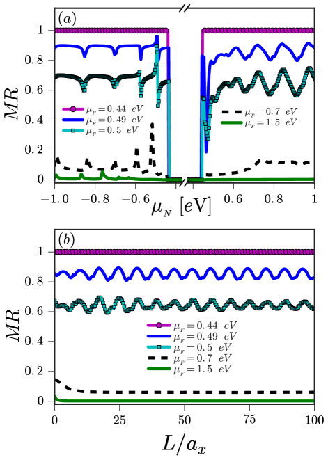
With the above-found behavior of the charge conductance, we evaluate the magnetoresistance of the proposed spin valve structure defined as the relative difference of the charge conductance in the two P and AP configurations, . The behavior of the resulting MR in terms of and the length of the N region are presented respectively in Figs. 5(a) and 5(b), for different values of . We observe that the spin valve effect can be perfect (with ) for the case of eV (). This perfect switching is robust with respect to an increase of the chemical potential of the N region. Increasing leads to the oscillatory behavior of the MR with respect to , such that the period and amplitude of the oscillations differ for the two cases of n-type and p-type doped N regions. The amplitude of the MR decreases with increasing and tends to zero for the highly doped F region. Note that the existence of a band gap in the dispersion of the monolayer phosphorene causes a gap in MR for ( defines the energy of the valance-band edge for the spin band). Moreover, it is shown in Fig. 5(b) that the perfect spin valve effect is preserved for large lengths of the N region, when eV. This is similar to the behavior of the pseudo-magnetoresistance in the monolayer-graphene-based pseudospin valve structure Majidi11 ; Majidi13 . For , MR shows an oscillatory behavior with respect to the value with the amplitude which decreases with and goes to zero for high values of . The oscillatory behavior of the MR with respect to the chemical potential and the length can be explained in the context of the Fabry-Prot oscillations Born , too.
III.3 Spin-transfer torque
.
.
Finally, we evaluate the behavior of the spin-transfer torque exerted on the magnetic order parameter of the right F region in the proposed F/N/F structure. Three-layer structures consisting of two magnetic layers separated by a conducting nonmagnetic spacer layer are well-known systems that exploit spin-transfer torque effects. When applying a charge current perpendicular to the layers, one of the magnetic layers, referred to as the pinned layer, acts as a spin polarizer. When the spin-polarized electrons reach the second layer, referred to as the free layer, they accumulate at the interface and thereby exert a torque onto the free layer.
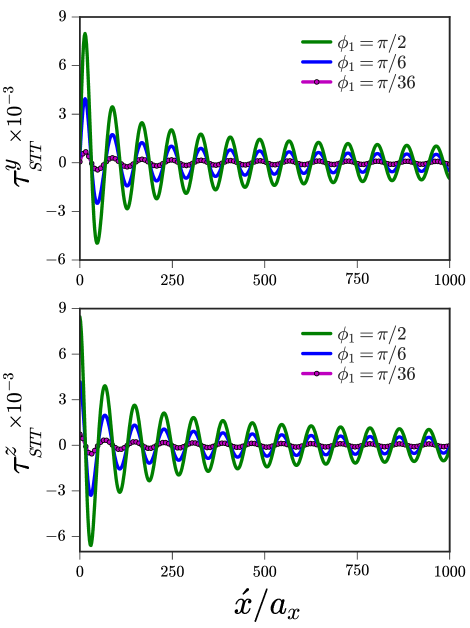
Figure 6 presents the dependence of the spin-transfer torques and (in units of ) on the distance () from the N/F interface for different values of . We fix , so that the component of the torque parallel to the magnetization of the right F region, , is zero. As seen, the total magnetic torque is not absorbed at the N/F interface and penetrates into the right F region. The torque components exhibit especially damped oscillatory behavior and their amplitudes diminish with decreasing . It is seen from Eqs. (II), (15), (16), and (17) that the torque components possess the terms proportional to which cause the conventional rapid oscillations on a length scale . These oscillations originate from the interference between electrons with opposite spin-indices. Moreover, we find that the amplitudes of the torque components decay with . The penetration of the spin transfer torque into the right F region in the phosphorene-based F/N/F structure is similar to that in the ferromagnetic superconductor- FS and graphene-based fnfgraphene1 spin valve structures, where the vast majority of the torque is absorbed in the interface region.
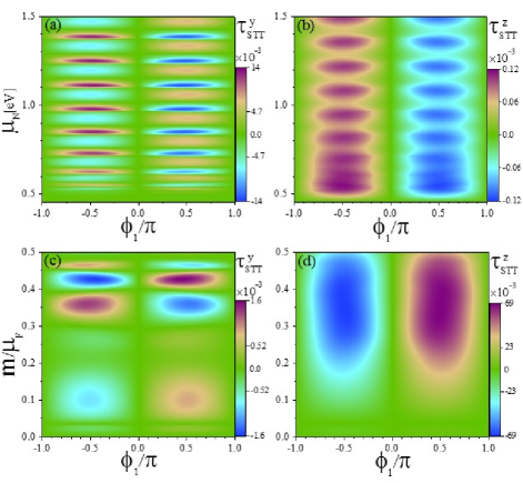
The top panel of Fig. 7 shows the behavior of the torque components absorbed at the N/F interface () in terms of and , when the magnetization orientation of the right F region is fixed to . The spin-transfer torque is seen to be an odd function of and oscillates with . The sign and magnitude of can be modulated by tuning with the gate voltage, while the sign of can-not be changed. Also, the magnitude of is two orders of magnitudes larger than . Interestingly, changing the exchange field value leads to the sign change of the torque in addition to its magnitude changes [see Fig. 7(c)]. However, the magnitude of the torque component increases with increasing the value, and can be two orders of magnitude larger than that of the . A large discrepancy between and originates from the anisotropic band structure of phosphorene. Note that in the graphene F/N/F structure, is qualitatively similar to fnfgraphene1 .
IV Conclusion
In conclusion, we have investigated the magnetotransport characteristics of a monolayer phosphorene ferromagnetic/normal/ferromagnetic (F/N/F) junction with noncollinear magnetization. We have found that the transmission probabilities of the incoming electrons from the spin and bands of the F region have different behavior by increasing the angle of incidence to the F/N/F structure with parallel (P) alignment of magnetization vectors, when the length of the N region is small. The transmission probability has a monotonically decreasing behavior with the incidence angle for an incoming -band electron, while a peak structure appears for an incident -band electron. Increasing the contact length leads to the appearance of a peak structure with unit transmission for the incoming -band electron and the enhancement of the peak number in the transmission probability of the incoming -band electron, while the transmission probabilities and , of both the incoming - and -band electrons to the proposed structure with anti-parallel (AP) alignment of magnetization have decreasing behavior with respect to the angle of incidence for small contact lengths and peak structures with the amplitudes for larger lengths . Also, applying a local gate voltage to the N region with large length amplifies the transmission probability at defined angles of incidence and attenuates it at other traveling modes in the corresponding F/N/F structure with the -doped N region.
Moreover, we have shown that the charge conductance of the proposed structure can be changed significantly by tuning the chemical potential of the N region , and the relative orientation of the magnetization directions in the two F regions. Interestingly, the charge conductance of the n-type doped F/N/F structure can be almost zero away from the AP configuration of magnetization, for determining ranges of the chemical potential of the F region . More importantly, it attains a minimum at the P configuration and a maximum near the AP configuration in the corresponding structure with -type doped N region. We have further demonstrated that the proposed structure exhibits a relative difference of the electrical resistance in the P and AP alignments of magnetization, which can be tuned to unity for defined values of . This perfect spin valve effect is more robust with respect to an increase of and is preserved even for large lengths of the N region. Furthermore, we have evaluated the equilibrium spin-transfer torque, which can be used to derive domain-wall motion in ferromagnetic materials, acting on the magnetization of the right F region. We have found that the total torque is not absorbed in the interface region, and both the magnitude and sign of the torque components can be controlled by tuning and the exchange field of the F region.
V Acknowledgement
This work is partially supported by Iran Science Elites Federation.
VI Appendix: spin-dependent transmission amplitudes
As said before, we calculate the transmission amplitudes and by matching the wave functions of the three regions of the left F region, the N region, and the right F region at the two interfaces, namely and . Those amplitudes read as
| (18) |
with
| (19) |
| (20) | |||||
| (21) |
| (22) | |||||
Finally, the spin-dependent transmission probabilities are obtained from the above relations as follows:
| (23) |
We mention that the transmission probabilities of the incoming spin -band electron, , can be obtained from the above formulas by replacing with , and vice versa.
References
- (1) L. Li, Y. Yu, G. J. Ye, Q. Ge, X. Ou, H. Wu, D. Feng, X. H. Chen and Y. Zhang, Nat. Nanotechnol. 9, 372 (2014).
- (2) H. Liu, A. T. Neal, Z. Zhu, Z. Luo, X. Xu, D. Tomanek, and P. D. Ye, ACS Nano 8, 4033 (2014).
- (3) A. Castellanos-Gomez, Nat. Photonics 10 202 (2016); F. Xia, H. Wang, D. Xiao, M. Dubey, and A. Ramasubramaniam, ibid, 8, 899 (2014).
- (4) H. Liu, Y. Du, Y. Deng, P. D. Ye, Chem. Soc. Rev. 44, 2732 (2015).
- (5) S. Das, M. Demarteau, A. Roelofs, ACS Nano 8, 11730 (2014).
- (6) M. V. Kamalakar, B. N. Madhushankar, A. Dankert, S. P. Dash, Small 11, 2209 (2015).
- (7) W. Lu, H. Nan, J. Hong, Y. Chen, C. Zhu, Z. Liang, X. Ma, Z. Ni, C. Jin, and Z. Zhang, Nano Res. 7, 853 (2014).
- (8) R. Fei and L. Yang, Nano Lett. 14, 2884 (2014).
- (9) X. Wang, A. M. Jones, K. L. Seyler, V. Tran, Y. Jia, H. Zhao, H. Wang, L. Yang, X. Xu, and F. Xia, Nat. Nanotechnol. 10, 517 (2015).
- (10) Y. Du, C. Ouyang, S. Shi, and M. Lei, J. Appl. Phys. 107, 093718 (2010).
- (11) V. Tran, R. Soklaski, Y. Liang, and L. Yang, Phys. Rev. B 89, 235319 (2014).
- (12) D. Çakir, H. Sahin, and F. M. Peeters, Phys. Rev. B 90, 205421 (2014).
- (13) L. Liang, J. Wang, W. Lin, B. G. Sumpter, V. Meunier, and M. Pan, Nano Lett. 14, 6400 6406 (2014).
- (14) A. S. Rodin, A. Carvalho, and A. H. Castro Neto, Phys. Rev. Lett. 112, 176801 (2014).
- (15) Z. Zhu, Ch. Li, W. Yu, D. Chang, Q. Sun, and Y. Jia, Appl. Phys. Lett. 105, 113105 (2014).
- (16) Y. Du, H. Liu, B. Xu, L. Sheng, J. Yin, C.-G. Duan, and X. Wan, Sci. Rep. 5, 8921 (2015).
- (17) G. Yang, S. Xu, W. Zhang, T. Ma, and C. Wu, Phys. Rev. B 94, 075106 (2016).
- (18) M. U. Farooq, A. Hashmi, and J. Hong, ACS Appl. Mater. Interfaces 7, 14423 (2015).
- (19) M. U. Farooq, A. Hashmi, and J. Hong, Sci. Rep. 6, 26300 (2016).
- (20) T. Hu and J. Hong, J. Phys. Chem. C 119, 8199 (2015).
- (21) X. Sui, C. Si, B. Shao, X. Zou, J. Wu, B.-L. Gu, and W. Duan, J. Phys. Chem. C 119, 10059 (2015).
- (22) L. Seixas, A. Carvalho, and A. H. Castro Neto, Phys. Rev. B 91, 155138 (2015).
- (23) I. Khan and J. Hong, New J. Phys. 17, 023056 (2015).
- (24) I. Zutić, J. Fabian, and S. Das Sarma, Rev. Mod. Phys. 76, 323 (2004).
- (25) L. Berger, Phys. Rev. B 54, 9353 (1996).
- (26) J. C. Slonczewski, J. Magn. Magn. Mater. 159, L1 (1996).
- (27) A. Brataas, A. D. Kent, and H. Ohno, Nat. Mater. 11, 372 (2012).
- (28) S. S. P. Parkin et al., J. Appl. Phys. 85, 5828 (1999); L. Thomas, G. Jan, J. Zhu, H. Liu, Y.-J. Lee, S. Le, R.-Y. Tong, K. Pi, Y.-J. Wang, D. Shen, R. He, J. Haq, J. Teng, V. Lam, K. Huang, T. Zhong, T. Torng, and P.-K. Wang, ibid, 115, 172615 (2014); K. Ando, S. Fujita, J. Ito, S. Yuasa, Y. Suzuki, Y. Nakatani, T. Miyazaki, and H. Yoda, ibid, 115, 172607 (2014).
- (29) J.-G. Zhu, X. Zhu, and Y. Tang, IEEE Trans. Magn. 44, 125 (2008); J.-G. Zhu, and Y. Wang, ibid. 46, 751 (2010).
- (30) A. A. Tulapurkar, Y. Suzuki, A. Fukushima, H. Kubota, H. Maehara, K. Tsunekawa, D. D. Djayaprawira, N. Watanabe, and S. Yuasa, Nature (London) 438, 339 (2005).
- (31) A. Fert, Rev. Mod. Phys. 80, 1517 (2008).
- (32) G. E. W. Bauer, E. Saitoh, and B. J. van Wees, Nat. Mater. 11, 391 (2012).
- (33) J. Linder, and J. W. A. Robinson, Nat. Phys. 11, 307 (2015).
- (34) M. N. Baibich, J. M. Broto, A. Fert, F. Nguyen Van Dau, F. Petroff, P. Etienne, G. Creuzet, A. Friederich, and J. Chazelas, Phys. Rev. Lett. 61, 2472 (1988).
- (35) G. Binasch, P. Grünberg, F. Saurenbach, and W. Zinn, Phys. Rev. B 39, 4828 (1989).
- (36) M. M. Glazov, P. S. Alekseev, M. A. Odnoblyudov, V. M. Chistyakov, S. A. Tarasenko, and I. N. Yassievich, Phys. Rev. B 71, 155313 (2005).
- (37) Z. Zheng, Y. Qi, D. Y. Xing, and J. Dong, Phys. Rev. B 59, 14505 (1999).
- (38) C. Ertler, and J. Fabian, Appl. Phys. Lett. 89, 242101 (2006).
- (39) N. Chatterji, A. A. Tulapurkar, and B. Muralidharan, Appl. Phys. Lett. 105, 232410 (2014).
- (40) H. S. Nguyen, D. Vishnevsky, C. Sturm, D. Tanese, D. Solnyshkov, E. Galopin, A. Lemaître, I. Sagnes, A. Amo, G. Malpuech, and J. Bloch, Phys. Rev. Lett. 110, 236601 (2013).
- (41) S. Yuasa, T. Nagahama, and Y. Suzuki, Science 297, 234 (2002).
- (42) A G. Petukhov, A. N. Chantis and D. O. Demchenko, Phys. Rev. Lett. 89, 107205 (2002).
- (43) S. Datta, Electronic transport in mesoscopic systems (Cambridge University Press, Cambridge, England, 1995); Y. V. Nazarov and Y. Blanter, Quantum Transport: Introduction to Nanoscience (Cambridge University Press, Cambridge, England, 2009)
- (44) T. Yokoyama and J. Linder, Phys. Rev. B 83, 081418 (2011).
- (45) J. Zou, G. Jin, and Y. Ma, J. Phys. Cond. Matt. 21, 126001 (2009).
- (46) R. Saxena, A. Saha, and S. Rao, Phy. Rev. B 92, 245412 (2015).
- (47) N. Tombros, C. Jozsa, M. Popinciuc, H. T. Jonkman, and B. J. van Wees, Nature (London) 448, 571 (2007).
- (48) H. Haugen, D. Huertas-Hernando, and A. Brataas, Phys. Rev. B 77, 115406 (2008).
- (49) A. G. Swartz, P. M. Odenthal, Y. Hao, R. S. Ruoff, and R. K. Kawakami, ACS Nano 6, 10063 (2012).
- (50) Z. Wang, C. Tang, R. Sachs, Y. Barlas, and J. Shi, Phys. Rev. Lett. 114, 016603 (2015).
- (51) V. K. Dugaev, V. I. Litvinov, and J. Barnas, Phys. Rev. B 74, 224438 (2006).
- (52) B. Uchoa, V. N. Kotov, N. M. R. Peres, and A. H. Castro Neto, Phys. Rev. Lett. 101, 026805 (2008).
- (53) O. V. Yazyev, Rep. Prog. Phys. 73, 056501 (2010).
- (54) M. Zare, B. Z. Rameshti, F. G. Ghamsari, and R. Asgari, Phys. Rev. B 95 045422 (2017).
- (55) M. Elahi, K. Khaliji, S. M. Tabatabaei, M. Pourfath and R. Asgari, Phys. Rev. B 91, 115412 (2015).
- (56) R. Landauer, IBM J. Res. Dev. 1, 223 (1957); 32, 306 (1988).
- (57) M. D. Stiles, A. Zangwill, Phys. Rev. B 66, 014407 (2002).
- (58) M. Born, and E. Wolf, Principles of Optics (Cambridge University Press, Cambridge, England, 1959).
- (59) L. Majidi, and M. Zareyan, Phys. Rev. B. 83, 115422 (2011).
- (60) L. Majidi, and M. Zareyan, J. Comput. Electron. 12, 134 (2013).
- (61) J. Linder, A. Brataas, Z. Shomali, and M. Zareyan, Phys. Rev. Lett. 109, 237206 (2012).