Wurtzite spin lasers
Abstract
Semiconductor lasers are strongly altered by adding spin-polarized carriers. Such spin lasers could overcome many limitations of their conventional (spin-unpolarized) counterparts. While the vast majority of experiments in spin lasers employed zinc-blende semiconductors, the room temperature electrical manipulation was first emonstrated in wurtzite GaN-based lasers. However, the underlying theoretical description of wurtzite spin lasers is still missing. To address this situation, focusing on (In,Ga)N-based wurtzite quantum wells, we develop a theoretical framework in which the calculated microscopic spin-dependent gain is combined with a simple rate equation model. A small spin-orbit coupling in these wurtzites supports simultaneous spin polarizations of electrons and holes, providing unexplored opportunities to control spin lasers. For example, the gain asymmetry, as one of the key figures of merit related to spin amplification, can change the sign by simply increasing the carrier density. The lasing threshold reduction has a nonmonotonic depenedence on electron spin polarization, even for a nonvanishing hole spin polarization.
I I. Introduction
Introducing spin-polarized carriers in semiconductor lasers offer an alternative path to realize spintronic applications, beyond the usually employed magnetoresistive effects Hallstein1997:PRB ; Ando1998:APL ; Rudolph2003:APL ; Holub2007:PRL ; Hovel2008:APL ; Basu2008:APL ; Basu2009:PRL ; Saha2010:PRB ; Fujino2009:APL ; Jahme2010:APL ; Gerhardt2011:APL ; Iba2011:APL ; Frougier2013:APL ; Frougier2015:OE ; Alharthi2015:APL ; Alharthi2015:APLb ; Hsu2015:PRB . Through carrier recombination, the angular momentum of the spin-polarized carriers is transferred to photons, thus leading to the circularly polarized emitted light Sinova2012:NM . Such spin lasers provide opportunity to extend the functionality of spintronic devices, as well to exceedthe performance of conventional (spin-unpolarized) lasers, from reducing the lasing threshold to improving their dynamical performance and digital operation Lee2010:APL ; Boeris2012:APL ; Lee2012:PRB ; Lee2014:APL ; Wasner2015:APL ; FariaJunior2015:PRB ; Hopfner2014:APL ; Lindemann2016:APL ; Pusch2015:EL .
Almost all spin lasers have been based on zinc-blende (ZB) semiconductors, such as GaAs or InAs, in which spin-dependent optical transitions were extensively studied for over 45 years Meier:1984 . However, a lone exception of a spin laser with an gain (active) region made of a wurtzite (WZ) semiconductor has so far also been the only case of an electrically manipulated spin laser at room temperature Chen2014:NN ; Zutic2014:NN . Unlike many theoretical studies of ZB spin lasers Gothgen2008:APL ; Holub2011:PRB ; FariaJunior2015:PRB , a theoretical description for WZ spin lasers is still missing. Focusing on WZ GaN-based quantum wells (QWs) as the gain region, we develop the first microscopic description of WZ spin lasers.
The significance of WZ materials for optical devices has been recognized by the 2014 Nobel prize in physics for an efficient blue light emitting diodes (LEDs). WZ-based optical devices using a direct band gap GaN and its In and Al alloys are ubiquitous in our daily lives, from efficient lightning to blue-ray disc readers. Due to their high electron saturation velocities and high breakdown voltages, GaN-based semiconductors are also promising for high-speed/high-power electronic devices Akasaki2015:RMP ; Amano2015:RMP ; Nakamura2015:RMP . However, for spin-dependent optical properties, WZ GaN does not appear encouraging, leading to only a negligibly small degree of a circular polarization of an emitted light which can be attributed to a rather weak spin-orbit coupling (SOC) Chen2005:APL . Therefore, the realization of the first electrically manipulated spin laser at room temperature using GaN-based gain region came as a surprise.
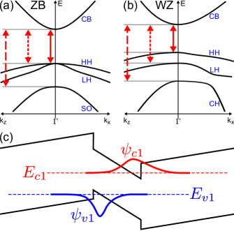
To better understand the differences between employing ZB and WZ semiconductors in optical devices, in Figs. 1(a) and (b) we show their bulk band structure and possible band edge optical transitions within the conventional Hamiltonians, using the typical notation: conduction band (CB), heavy holes (HH), light holes (LH) and spin-orbit split-off holes (SO) for ZB Winkler:2003 ; Lee2014:PRB and CB, HH, LH and crystal-field split-off hole (CH) for WZ Chuang1996:PRB . Each of the marked dipole transitions has a different amplitude for specific spins that apply both to radiative recombinations and excitations.
If we denote the photon density of positive (negative) helicity by (), we can describe the relevant helicity in each of the transitions. For example, in the CB-HH transition spin up (down) leads to (), in CB-LH spin up (down) leads to (), while in CB-SO for ZB, or CB-CH for WZ, spin up (down) leads to (). For ZB the amplitude of helicity contributions are fixed: , . The electron spin polarization in terms of spin up (down) electron density (),
| (1) |
arising from optical spin injection (HH/LH-CB) yields , a well-known result at the band gap, neglecting electron spin relaxation Pierce1975:PLA ; Zutic2004:RMP . In contrast, for WZ the corresponding amplitudes depend on the materials parameters related to the SOC Chuang1996:PRB ,
| (2) |
where the energy is expressed as,
| (3) |
in terms of the crystal field splitting energy and SOC splitting energies . With removed HH and LH degeneracy at the wavevector (-point) in WZ semiconductors [see Fig. 1(b)], one would expect % optical spin injection at the band gap, overcoming the 50% limitation of ZB materials Zutic2004:RMP . However, due to the relatively weak SOC in nitride-based materials note:GaN , the energy separation for the topmost valence bands is typically 10-20 meV, comparable to the energy of the broadening effects by impurities and room temperature, ultimately leading to inefficient optical spin injection Chen2005:APL . In GaN-based spin LEDs only a small circular polarization of electroluminescence was detected at 200 K Banerjee2013:APL as well as at 300 K in the applied magnetic field Chen2010:APL . These limitations could be overcome in electrical spin injection or extraction, as shown (In,Ga)N/GaN-based nanodiscs and nanorods covered by FeO nanoparticles Chen2014:NL ; Chen2014:NN ; Zutic2014:NN .
In this study, we investigate WZ spin lasers with /GaN QWs as their gain region using microscopic band structure calculations. While a weak SOC retains desirable spin-dependent properties of optical gain, it also necessitates simultaneous consideration of electron and hole spin polarizations, largely overlooked in the previous studies. By combining macroscopic rate equations with microscopic gain calculations based on a method, we establish a versatile method to describe spin lasers which extends the strengths of the two complementary approaches.
In Sec. II we describe the method to evaluate the electronic structure of (In,Ga)N QW which is used in Sec. III to calculate microscopic spin-dependent optical gain. In Sec. IV we combine these microscopic gain calculations with simple rate equations, suitable to describe various dynamical phenomena in spin lasers. In Sec. V we discuss future opportunities to apply our theoretical framework to other systems.
II II. Quantum well electronic structure
An important consequence of the atomic arrangement of WZ materials along the [0001] direction is the presence of the polarization fields. A relative displacement between cations and anions in the unit cell leads to the spontaneous polarization along the growth direction in QWs. Under external applied strain this cation-anion displacement is modified and also yields piezoelectric polarization note:pols . Such polarization fields are schematically shown in Fig. 1(c) for a WZ QW. The response of the quantum confined states to the static electric field is known as the quantum confined Stark effect and recognized as a very efficient mechanism to tune the optical transitions in semiconductor nanostructures Chuang:2009 . These polarization fields modify both electronic levels as well as change the spatial electron-hole separation and thus the overlap integral between CB and VB wave functions.
Within the method combined with the envelope function approximation, and including the polarization effects, the total Hamiltonian of the QW system is,
| (4) |
with the growth axis along the direction (the axis, or [0001] direction, of the WZ structure). The Hamiltonian denotes the term, describes the strain, includes the band-offset at the interface that generates the QW energy profile, and includes the potential profile due to spontaneous and piezoelectric polarizations. In this study, we considered the Hamiltonian for WZ materials with explicit interaction between CB and VB which gives rise to the dipole coupling for optical transitions. The specific definitions of these Hamiltonians are described in Refs. FariaJunior2012:JAP ; Miao2012:PRL ; FariaJunior2014:JAP . In order to numerically solve the resulting system of coupled differential equations from Eqs. (4), we apply the plane wave expansion discussed in Refs. Sipahi1996:PRB ; Lee2014:PRB ; FariaJunior2012:JAP ; FariaJunior2014:JAP ; FariaJunior2015:PRB .
For the gain region of the laser we consider a 3 nm thick single strained QW, surrounded by 6 nm GaN barriers, the typical lengths and composition of (In,Ga)N-based vertical cavity surface emitting lasers (VCSELs) Lu2008:APL ; Lu2010:APL ; Kasahara2011:APE ; Lin2014:LPL . The bulk InN and GaN parameters are obtained from Ref. Miao2012:PRL , we use their linear interpolation for the alloy and the bowing parameter for the band gap, Vurgaftman2001:JAP . The interface band offsets are and Dong2013:JAP . We choose at T = 300 K with Varshni parameters and the refractive indexes from Refs. Vurgaftman2001:JAP ; note:web .
To develop some intuition about the relevant SOC parameters in (In,Ga)N QWs, we recall that in GaAs, as the representative ZB semiconductor, at the -point HH and LH are degenerate and separated by eV Vurgaftman2001:JAP from the SO band. It is helpful to think of ZB GaAs as a WZ structure without crystal-field splitting energy () and a much larger SOC that yields Park2000:JAP ; FariaJunior2012:JAP . For the GaN barrier, and , and for the QW material , and . In the bulk case, such values of provide an energy difference at the -point in GaN of 5.1 meV for HH-LH and 21.9 meV for HH-CH. For the energy differences are 6 meV and 22.9 meV for HH-LH and HH-CH, respectively. QW confinement and polarization fields can provide larger energy separations for the different wave functions (no nodes, one node, etc). However, the typical HH-LH QW states separation with same number of nodes remains similar to the bulk energy values.
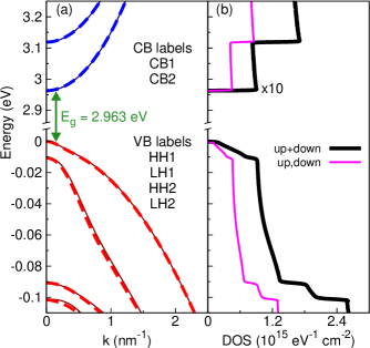
The resulting band structure of /GaN QW, is presented in Fig. 2(a), showing the two confined conduction subbands, CB1 and CB2, and the top four confined valence subbands, HH1, LH1, HH2 and LH2, labeled according to the dominant component of the total envelope function Chuang1996:APL . Each subband is twofold degenerate in and for nonzero values the effect of the asymmetric polarization field creates small spin splittings in the valence subbands note:spinsplittings , lifting Kramers degeneracy Park2000:JAP . Considering optical transitions at room temperature (25 meV), the spin splittings are negligible as if the bands were twofold degenerate. Furthermore, because of the energy separation of 150 (80) meV from CB1 (LH1) to CB2 (HH2) subbands, we can expect the emission range of the gain spectra to be ruled by CB1-HH1 () and CB1-LH1 () transitions. The corresponding density of states (DOS) shown in Fig. 2(b), confirms that spin-resolved DOS has equal contributions for spin up and spin down.
III III. Microscopic spin-dependent gain
Obtained electronic structure with the corresponding carrier populations provides the starting point to microscopically calculate the optical gain depicted in Fig. 3, the hallmark of lasers. The resulting gain coefficient (or gain spectrum) is the negative value of the absorption coefficient and is calculated as Haug:2004 ; Chuang:2009 ,
| (5) |
where the summation indices and label the conduction and valence subbands, respectively is the interband dipole transition amplitude for the polarization of light , is the Fermi-Dirac distribution for the electron occupancy in the conduction (valence) subbands, is the Planck’s constant, is the interband transition frequency, and is the Dirac delta-function, which is often replaced to include broadening effects for finite lifetimes Chuang:2009 ; Chow:1999 . In the constant , is the vacuum permittivity, is the speed of light (to distinguish it from the CB index), is the dominant real part of the refractive index of the material, is the electron charge, is the free electron mass, and is the QW volume.
Similar to ZB GaAs-based spin lasers Holub2011:PRB ; FariaJunior2015:PRB , the dipole selection rules for the interband optical transitions are spin-conserving, i. e., the dipole matrix element does not change spin. Therefore, the gain coefficient for the light polarization includes independent contributions of spin-up and spin-down carriers,
| (6) |
denoted by the subscripts and , respectively.
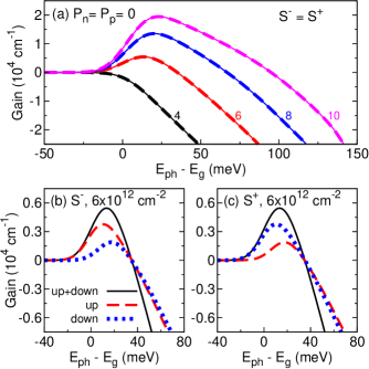
To develop intuition and understand the role of SOC in the optical transitions, we first illustrate the gain spectra on the example of conventional lasers. This implies injecting vanishing electron and hole spin polarization, , where the expression for is analogous to Eq. (1). In Fig. 4(a) we show such a gain spectra as function of photon energy for various carrier densities.
For calculated gain spectra in (In,Ga)N QWs it is customary to include various broadening effects. In addition to the homogeneous broadening, frequently used in ZB QWs Chow:1999 ; FariaJunior2015:PRB , parametrized here by with 10 meV full width at half-maximum (FWHM), we also consider an inhomogeneous Gaussian broadening, attributed to compositional and potential fluctuations. Our choice of Gaussian broadening with 20 meV FWHM is consistent with a decreased broadening for smaller emission wavelengths in (In,Ga)N QW lasers and reported values relevant for wavelengths of 415 nm Funato2013:APE which corresponds to the typical energy of the gain peak in our calculations.
Because of the broadening effects, the individual CB1-HH1 and CB1-LH1 transitions that dominate the gain spectra cannot be distinguished [HH1 and LH1 are 10 meV apart, see Fig. 2(a)]. On the other hand, by analyzing the spin-resolved gain we can identify different contributions of CB1-HH1 and CB1-LH1 transitions. In Figs. 4(b) and 4(c) we show the gain spectra decomposed in spin up and spin down transitions at for and light polarization, respectively. For the total gain we have which requires and FariaJunior2015:PRB , as could be seen in Figs. 4(b) and 4(c). Due to the small SOC energy in nitrides, the () gain peak of spin up (down) CB1-HH1 transition is twice as large as the spin down (up) CB1-LH1 transition. For a larger SOC energy, this ratio would increase. For example, in ZB GaAs spin laser FariaJunior2015:PRB , this ratio is 6 (for a SOC energy of 114 meV, compared to meV in nitrides).
We next turn to the gain properties in spin-lasers where injected carriers are spin-polarized. Guided by the typical spin dynamics for ZB semiconductors in which hole spin relaxes nearly instantaneously, previous studies have largely focussed on spin lasers with nonzero , but vanishing . However, since the degeneracy of HH and LH in bulk WZ semiconductors is lifted by the crystal field potential, the spin relaxation times of holes in GaN could be comparable to those of electrons Brimont2009:JAP . This is in stark contrast to bulk GaAs where at 300 K the hole spin relaxation time is three to four orders of magnitude shorter than for electrons Zutic2004:RMP . We therefore also consider the effect of nonzero , excluded in the two prior microscopic studies of gain spectra in spin lasers Holub2011:PRB ; FariaJunior2015:PRB .
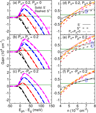
The gain for WZ spin lasers is shown in Fig. 5 as a function of photon energy and carrier density. These results confirm that the gain becomes helicity-dependent, , as known from ZB spin lasers. However, the role of simultaneous presence of nonvanishing and requires further attention. With fixed we see that a change from to [panels (a) and (b)] enhances the difference between the gain contribution for and , while a change from to [panels (a) and (c)] reduces such a difference.
Since equal but opposite electron spin polarizations [, Fig. 5(c)] describe the vanishing total spin in the gain region, it is helpful to note another realization of a vanishing total spin in Fig. 4(a). Nevertheless, the gain spectra in these two cases are slightly different which can be attributed to the different features of CB and VB including their curvature, number of confined bands, and DOS. Thus, the difference between the gain contribution for and cannot be eliminated for .
A complementary information about the calculated gain is given with its density dependence in Figs. 5(d)-(f). The results are shown for photon energies, corresponding to the CB1-HH1 and CB1-LH1 transitions [recall Fig. 2] which can be individually favored by the cavity design in a single-mode VCSEL Michalzik:2013 . Several trends can be inferred. For example, a nonlinear gain-dependence on density is different for the two photon energies. With an increased carrier density, CB1-LH1 transition provides larger gain values than as compared to CB1-HH1. While a reference curve (long dashed) for the gain of a conventional laser is lower than for and [panels (d) and (e)], the situation is reversed above the gain threshold (green horizontal line) for [panel (f)] where at larger density is possible.
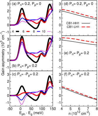
To better understand the helicity-dependent gain, it is useful to calculate the corresponding gain asymmetry,
| (7) |
an important figure of merit in spin lasers. Considering that lasers have nonlinear light-injection characteristics, such gain asymmetry could enable robust spin filtering or spin amplification Gothgen2008:APL . Close to the lasing threshold even a small carrier spin polarization in the gain region can lead to completely circularly polarized emitted light Iba2011:APL .
The results for the gain asymmetry, extracted from Fig. 5, are shown in Fig. 6 as a function of the photon energy and the carrier density. While a large is desirable, it is crucial that it corresponds to the regime. For example, the largest in Figs. 5(a) and (c) is found for photon energies of 125 - 140 meV above the band gap. However, as seen in Figs. 5(a) and (c), this range corresponds to the absorption regime () and such does not influence the emitted light. As and vary, the largest useful is found slightly above the gap. As shown in Figs. 6(d)-(f), to enhance a lower density and CB1-LH1 are slightly better. An interesting deviation from these trends is seen in Fig. 6 for . Near the band gap, an increase in leads to the sign change of and its maximum magnitude in the regime for the larges shown carrier density. This behavior points to yet unexplored opportunities to optimize the operation of spin lasers with a simultaneous spin polarization of electrons and holes.
Our results show that despite the small SOC energy of WZ nitrides, considered detrimental for optical spin injection, the gain asymmetry remains robust. Another important figure of merit of spin lasers is their threshold reduction, the lasing operation could be attained at lower injected carrier density than in conventional lasers. We will analyze this behavior in the next section.
IV IV. Rate equations
Here we briefly review a complementary approach based on rate equations (REs) and discuss how its understanding can be enhanced from our microscopic gain calculations. REs have been successfully used to describe both conventional and spin lasers Chuang:2009 ; Michalzik:2013 ; Coldren:2012 ; Zutic:2011 . An advantage of this approach is its simplicity. REs can provide a direct relation between material characteristics and device parameters, as well as often allowing analytical solutions and an effective method to elucidate many trends in the operation of lasers Chuang:2009 ; Coldren:2012 . With notation widely used for conventional lasers Chuang:2009 ; Coldren:2012 , generalized to include spin- and helicity-resolved quantities, we can write REs as Lee2014:APL ; Wasner2015:APL ,
| (8) | |||
| (9) | |||
| (10) |
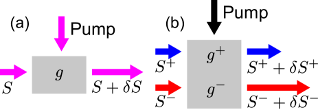
In the gain term, , is the transparency density, and is the gain compression factor Chuang:2009 ; Coldren:2012 , ensuring that the output light does not increase indefinitely with injection , is the gain parameter, and is the optical confinement factor. The electron spin relaxation is given by , where is the electron spin relaxation time ( for holes) Zutic2003:APL . The carrier recombination can have various dependences on carrier density Gothgen2008:APL and be characterized by a carrier recombination time . is the fraction of the spontaneous recombination producing light coupled to the resonant cavity, and is the photon lifetime, to model optical losses Rudolph2003:APL ; Holub2007:PRL ; Gothgen2008:APL .
While the method does not include spin relaxation (, ), similar dynamical effects are easily included in REs. However, REs rely on various input parameters that can be obtained from experiments or microscopic calculations. A more complete description of spin lasers can be therefore developed by combining the method and the macroscopic RE model. We illustrate this approach by focusing on the optical gain in WZ spin lasers. Specifically, the gain parameter and the transparency density in the gain term in REs, can be obtained by fitting, for each and , the carrier density dependence of the calculated microscopic gain presented in Figs. 5(d)-(f).
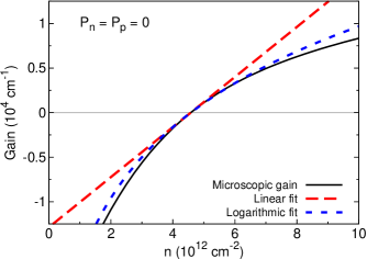
Following the REs for spin lasers Rudolph2003:APL ; Holub2007:PRL ; Gothgen2008:APL ; Lee2014:APL ; Wasner2015:APL we use a simple linear dependence of gain on the carrier density to provide a better comparison with the published work. This is illustrated in Fig. 7 for calculated gain of a conventional WZ laser. In the linear fit, the slope of the gain at (where ) in REs is matched with the slope of the calculated gain. However, we note that the logarithmic gain model, often used in conventional QW lasers Chuang:2009 , would be a better fit. Another difference between REs and the calculated gain is the helicity-dependent gain coefficient (recall Figs. 5 and 6) and we include that behavior by fitting the RE gain for each helicity separately. To follow the method we choose , , rather than seeking the best possible fit between the two methods. Likewise, we choose even though the gain compression could give a better agreement at larger . The remaining RE parameters are assigned from the previous work Arif2008:IEEEJQE .
Unlike a single lasing threshold, , in conventional lasers, with spin-dependent gain, there are two lasing thresholds in spin lasers, which delimits three operating regimes Gothgen2008:APL : (i) For a spin LED regime, (ii) For there is a spin-filtering regime and the lasing with only one helicity. (iii) For , there is a lasing with both helicities. It is then convenient to define the threshold reduction,
| (11) |
as an important figure of merit that influences both the steady-state and dynamical operation of spin lasers Lee2010:APL .
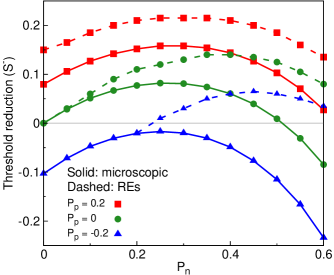
In Fig. 8 we compare the threshold reduction as a function of electron spin polarization calculated using the microscopic method and REs, for several values of hole spin polarization. Despite noticeable differences between the two methods, they both show an overall nonmonotonic dependence of on , preserved for each . It is instructive to note that previously studied REs with and fixed yield a monotonic increase in with , from at to at Gothgen2008:APL . However, using REs with a linear fit of the gain for at each shows in Fig. 8 a much closer agreement to the microscopic gain results and, by constructions, the two methods coincide at .
Including the hole spin polarization, the disagreement between the two methods is more pronounced for , than for . The corresponding RE results largely fail to capture the calculated threshold increase (, reported also in ZB lasers Holub2011:PRB ; FariaJunior2015:PRB ) and are not properly defined for . To explore why the RE results for are worse, it is useful to recall the dipole optical selection rules for transitions sketched in Fig. 1. In our notation that means that both spontaneous and stimulated recombination (optical gain) involve only electrons and holes of the same spin. For example, spontaneous radiative recombination has terms or note:recombine . However, in Eqs. (9) or (10) the gain term does not accurately respect these selection rules. For a sufficiently large carrier density the lasing would occur, even if the carrier spins are not compatible with the selection rules. When and have the opposite sign there are more carriers having a “wrong spin” to satisfy the selection rules leading to a worse agreement with the microscopic results. Such a disagreement would be less pronounced for shorter spin relaxation times, allowing “wrong spin carriers” to recombine while respecting the selection rules.
It is also possible to address the missing RE data for . In the steady-state, Eq. (10) implies,
| (12) |
In the operating regime (iii): , both helicities lase and are large, which yields, , Therefore, . Together with the charge neutrality, we have and , which means that is guaranteed in the regime (iii). This is relevant for the case and , because emitted is associated with minority instead of majority spin, such that the lasing of is in the regime (iii). The required in the third regime thus reduces the freedom of a realizable spin polarization in REs.
V V. Conclusions
Our framework of combining microscopic gain calculations with simple rate equations provides predictive and computationally inexpensive materials-specific approach to explore spin lasers. The choice of wurtzite lasers was guided by the first realization of an electrically manipulated spin laser at room temperature Chen2014:NN and the absence of any prior theoretical work. In contrast to zinc-blende GaAs, in wurtzite GaN there is a much smaller spin-orbit coupling, usually considered as a detrimental situation for optical spin injection. We have shown that even such a small spin-orbit coupling in wurtzites yields robust signatures of a spin-dependent gain, including the gain asymmetry, desirable for spin lasers. With the presence of nonvanishing electron and hole spin polarization, largely overlooked in the previous studies, the gain asymmetry can even change its sign by simply increasing the carrier density. The lasing threshold reduction has a nonmonotonic depenedence on electron spin polarization, even for a nonvanishing hole spin polarization.
While a weak spin-orbit coupling is expected to lead to an enhanced spin relaxation times, this is not the case for GaN which has a defect dominated spin-relaxation and electron spin relaxation times about an order of magnitude shorter than in GaAs Brimont2009:JAP ; Bhattacharya2016:APL . Although materials advances could enable longer spin relaxation times in GaN, the current values are already suitable for digital and high-frequency operation of spin lasers Lee2014:APL ; Wasner2015:APL .
The present framework can be adapted for other materials and laser geometries. With an increasing interest in non-nitride III-V wurtzite materials with large spin-orbit coupling De2010:PRB ; Cheiwchanchamnangij2011:PRB ; FariaJunior2016:PRB ; Gmitra2016:PRB , we expect they could facilitate optically-injected spin lasers at room temperature. While we have focused on spin VCSELs, our approach would also be useful for vertical external cavity surface emitting lasers (VECSELs)Frougier2015:OE ; Frougier2013:APL . They enable depositing a thin-film ferromagnet just 100-200 nm away from the gain region for spin injection at the room temperature. Various spin and phonon lasers can also be implemented using intraband transitions within the conduction band Khaetskii2013:PRL or in metallic systems Korenivski2013:EPL ; Naidyuk2012:NJP . It would be interesting to develop a suitable description for them by combining microscopic gain calculations and simple rate equations.
An important materials challenge for the advances in wurtzite spin lasers would be to establish magnetic regions and their detailed theoretical description for robust electrical spin injection into the gain region. In zinc-blende semiconductors a number of such materials are already available Zutic2004:RMP ; Fabian2007:APS ; Hanbicki2002:APL ; Zega2006:PRL ; Salis2005:APL . In addition to demonstrating that Fe3O4 nanomagnets are suitable for wurtzite spin lasers Chen2014:NN , many other opportunities could be explored. For example, ferromagnetic semiconductors provide electrically- and optically-controlled magnetic properties Zutic2004:RMP ; Koshihara1997:PRL ; Ohno2000:N ; Dietl2014:RMP ; DiasCabral2011:PRB , while supporting ultrafast optical processes Wang2006:JPCM . With a thin barrier region, even simple ferromagnets may enable tunable carrier spin polarization relying on gate-controlled magnetic proximity effects Lazic2016:PRB .
We thank N. C. Gerhardt for valuable discussions of the optical gain. This work was supported by NSF ECCS-1508873, U.S. ONR N000141310754, FAPESP Grants No. 2012/05618-0, 2011/19333-4, CNPq Grants No. 304289/2015-9, 246549/2012-2, CAPES-CsF 88887.125287/2015-00, and MOST-105-2811-M-147, Taiwan, Republic of China.
References
- (1) S. Hallstein, J. D. Berger, M. Hilpert, H. C. Schneider, W. W. Rühle, F. Jahnke, S. W. Koch, H. M. Gibbs, G. Khitrova, and M. Oestreich, Phys. Rev. B 56, R7076 (1997).
- (2) H. Ando, T. Sogawa, and H. Gotoh, Appl. Phys. Lett. 73, 566 (1998).
- (3) J. Rudolph, D. Hägele, H. M. Gibbs, G. Khitrova, and M. Oestreich, Appl. Phys. Lett. 82, 4516 (2003); J. Rudolph, S. Döhrmann, D. Hägele, M. Oestreich, and W. Stolz, Appl. Phys. Lett. 87, 241117 (2005).
- (4) M. Holub, J. Shin, D. Saha, and P. Bhattacharya, Phys. Rev. Lett. 98, 146603 (2007).
- (5) S. Hövel, A. Bischoff, and N. C. Gerhardt, M. R. Hofmann, and T. Ackemann, A. Kroner, and R. Michalzik, Appl. Phys. Lett. 92, 041118 (2008).
- (6) D. Basu, D. Saha, C. C.Wu, M. Holub, Z. Mi, and P. Bhattacharya, Appl. Phys. Lett. 92, 091119 (2008).
- (7) D. Basu, D. Saha, and P. Bhattacharya, Phys. Rev. Lett. 102, 093904 (2009).
- (8) D. Saha, D. Basu, and P. Bhattacharya, Phys. Rev. B 82, 205309 (2010).
- (9) H. Fujino, S. Koh, S. Iba, T. Fujimoto, and H. Kawaguchi, Appl. Phys. Lett. 94, 131108 (2009).
- (10) M. Li, H. Jähme, H. Soldat, N. C. Gerhardt, M. R. Hofmann, and T. Ackemann, A. Kroner, and R. Michalzik Appl. Phys. Lett. 97, 191114 (2010).
- (11) N. C. Gerhardt, M. Y. Li, H. Jähme, H. Höpfner, T. Ackemann, and M. R. Hofmann, Appl. Phys. Lett. 99, 151107 (2011).
- (12) S. Iba, S. Koh, K. Ikeda, and H. Kawaguchi, Appl. Phys. Lett. 98, 081113 (2011).
- (13) J. Frougier, G. Baili, M. Alouini, I. Sagnes, H. Jaffrès, A. Garnache, C. Deranlot, D. Dolfi, and J.-M. George, Appl. Phys. Lett. 103, 252402 (2013).
- (14) J. Frougier, G. Baili, I. Sagnes, D. Dolfi, J.-M. George, and M. Alouini, Opt. Expr. 23, 9573 (2015).
- (15) S. S. Alharthi, A. Hurtado, V.-M. Korpijarvi, M. Guina, I. D. Henning, and M. J. Adams, Appl. Phys. Lett. 106, 021117 (2015).
- (16) S. S. Alharthi, J. Orchard, E. Clarke, I. D. Henning, and M. J. Adams, Appl. Phys. Lett. 107, 151109 (2015).
- (17) F.-k. Hsu, W. Xie, Y.-S. Lee, S.-D. Lin, and C.-W. Lai, Phys. Rev. B 91, 195312 (2015).
- (18) J. Sinova and I. Žutić, Nature Mater. 11, 368 (2012).
- (19) J. Lee, W. Falls, R. Oszwałdowski, and I. Žutić, Appl. Phys. Lett. 97, 041116 (2010).
- (20) G. Boéris, J. Lee, K. Výborný, and I. Žutić, Appl. Phys. Lett. 100, 121111 (2012).
- (21) J. Lee, R. Oszwałdowski, C. Gøthgen, and I. Žutić, Phys. Rev. B 85, 045314 (2012).
- (22) J. Lee, S. Bearden, E. Wasner, and I. Žutić, Appl. Phys. Lett. 105, 042411 (2014).
- (23) E. Wasner, S. Bearden, J. Lee, and I. Žutić, Appl. Phys. Lett. 107, 082406 (2015).
- (24) P. E. Faria Junior, G. Xu, J. Lee, N. C. Gerhardt, G. M. Sipahi, and I. Žutić, Phys. Rev. B 92, 075311 (2015).
- (25) H. Höpfner, M. Lindemann, N. C. Gerhardt, and M. R. Hofmann, Appl. Phys. Lett. 104, 022409 (2014).
- (26) M. Lindemann, T. Pusch, R. Michalzik, N. C Gerhardt, and M. R. Hofmann, Appl. Phys. Lett. 108, 042404 (2016).
- (27) T. Pusch, M. Lindemann, N. C. Gerhardt, M. R. Hofmann, and R. Michalzik, Electron. Lett. 51, 1600 (2015).
- (28) Optical Orientation, edited by F. Meier and B. P. Zakharchenya (North-Holland, New York, 1984).
- (29) J.-Y. Chen, T.-M. Wong, C.-W. Chang, C.-Y. Dong, and Y.-F Chen, Nat. Nanotech. 9, 845 (2014).
- (30) I. Žutić and P. E. Faria Junior, Nat. Nanotech. 9, 750 (2014).
- (31) C. Gøthgen, R. Oszwałdowski, A. Petrou, and I. Žutić, Appl. Phys. Lett. 93, 042513 (2008).
- (32) M. Holub and B. T. Jonker, Phys. Rev. B 83, 125309 (2011).
- (33) I. Akasaki, Rev. Mod. Phys. 87, 1119 (2015).
- (34) H. Amano, Rev. Mod. Phys. 87, 1133 (2015).
- (35) S. Nakamura, Rev. Mod. Phys. 87, 1139 (2015).
- (36) W. M. Chen, I. A. Buyanova, K. Nishibayashi, Kayanuma, K. Seo, A. Murayama, Y. Oka, G. Thaler, R. Frazier, C. R. Abernathy, F. Ren, S. J. Pearton, C.-C. Pan, G.-T. Chen and J.-I Chyi, Appl. Phys. Lett. 87, 192107 (2005).
- (37) R. Winkler, Spin-orbit Coupling Effects in Two-Dimensional Electron and Hole Systems, (Springer, New York, 2003).
- (38) J. Lee, K. Výborný, J. E. Han, and I. Žutić, Phys. Rev. B 89, 045315 (2014).
- (39) S. L. Chuang and C. S. Chang, Phys. Rev. B 54, 2491 (1996).
- (40) D. Pierce, F. Meier and P. Zürcher, Phys. Lett. A 51, 465 (1975).
- (41) I. Žutić, J. Fabian, and S. Das Sarma, Rev. Mod. Phys. 76, 323 (2004).
- (42) In stark contrast to very dilute ZB nitrides with strong SOC, such as Ga0.67In0.33N0.016As0.984 QW-based spin lasers, K. Schires, R. A. Seyab, A. Hurtado, V.-M. Korpijärvi, M. Guina, I. D. Henning, and M. J. Adams, Opt. Expr. 20, 3550 (2012).
- (43) D. Banerjee, R. Adari, S. Sankaranarayan, A. Kumar, S. Ganguly, R. W. Aldhaheri, M. A. Hussain, A. S. Balamesh, and D. Saha, Appl. Phys. Lett. 103, 242408 (2013).
- (44) L.-C. Chen, C.-H. Tien, and C.-S. Mu, Opt. Expr. 18, 2302 (2010).
- (45) J. Y. Chen, C. Y. Ho, M. L. Lu, L. J. Chu, K. C. Chen, S. W. Chu, W. Chen, C. Y. Mou, and Y.-F. Chen, Nano Lett. 14, 3130 (2014).
- (46) See, for example, Chapter 3 of Nitride Semiconductor Devices: Principles and Simulation, edited by J. Piprek (Wiley, Weinheim, 2007).
- (47) S. L. Chuang, Physics of Optoelectronic Devices, 2 Edition (Wiley, New York, 2009).
- (48) P. E. Faria Junior and G. M. Sipahi, J. Appl. Phys. 112, 103716 (2012).
- (49) M. S. Miao, Q. Yan, C. G. Van de Walle, W. K. Lou, L. L. Li, and K. Chang, Phys. Rev. Lett. 109, 186803 (2012).
- (50) P. E. Faria Junior, T. Campos, and G. M. Sipahi, J. Appl. Phys. 116, 193501 (2014).
- (51) G. M. Sipahi, R. Enderlein, L. M. R. Scolfaro and J. R. Leite, Phys. Rev. B 53, 9930 (1996).
- (52) T.-C. Lu, C.-C. Kao, H.-C. Kuo, G.-S. Huang and S.-C. Wang, Appl. Phys. Lett. 92, 141102 (2008).
- (53) T.-C. Lu, S.-W. Chen, T.-T. Wu, P.-M. Tu, C.-K. Chen, C.-H. Chen, Z.-Y. Li, H.-C. Kuo and S.-C. Wang, Appl. Phys. Lett. 97, 071114 (2010).
- (54) D. Kasahara, D. Morita, T. Kosugi, K. Nakagawa, J. Kawamata, Y. Higuchi, H. Matsumura and T. Mukai, Appl. Phys. Expr. 4, 072103 (2011).
- (55) B. C. Lin, Y. A. Chang, K. J. Chen, C. H. Chiu, Z. Y. Li, Y. P. Lan, C. C. Lin, P. T. Lee, Y. K. Kuo, M. H. Shih, H. C. Kuo, T. C. Lu and S. C. Wang, Laser Phys. Lett. 11, 085002 (2014).
- (56) I. Vurgaftman, J. R. Meyer and L. R. Ram-Mohan, J. Appl. Phys. 89, 5815 (2001).
- (57) L. Dong, J. V. Mantese, V. Avrutin, Ü Özgür, H. Morkoç and S. P. Alpay, J. Appl. Phys. 114, 043715 (2013).
- (58) http://www.ioffe.ru/SVA/NSM/Semicond/
- (59) S. L. Chuang and C. S. Chang, Appl. Phys. Lett. 68, 1657 (1996).
- (60) The VB spin splitting appears because of the off-diagonal SOC energy in the Hamiltonian that mediates the coupling between the asymmetric potential and -dependent terms. Within this model the CB has no SOC interaction with other bands, therefore the spin splitting is not seen in the CB structure.
- (61) S. H. Park and S. L. Chuang, J. Appl. Phys. 87, 353 (2000).
- (62) H. Haug and S. W. Koch, Quantum Theory of Optical and Electronic Properties of Semiconductors, 4 Edition (World Scientific Publishing, Singapore, 2004).
- (63) W. W. Chow and S. W. Koch, Semiconductor-Laser Fundamentals: Physics of the Gain Materials, (Springer, New York, 1999).
- (64) M. Funato, Y. S. Kim, Y. Ochi, A. Kaneta, Y. Kawakami, T. Miyoshi and S. Nagahama, Appl. Phys. Express 6, 122704 (2013).
- (65) C. Brimont, M. Gallart, A. Gadalla, Olivier Crégut, Bernd Hönerlage, and P. Gilliot, J. Appl. Phys. 105, 023502 (2009).
- (66) VCSELs Fundamentals, Technology and Applications of Vertical-Cavity Surface-Emitting Lasers, edited by R. Michalzik (Springer, Berlin, 2013).
- (67) L. A. Coldren, S. W. Corzine, and M. L. Mašović, Diode Lasers and Photonic Integrated Circuits, 2 Edition (Wiley, Hoboken, 2012).
- (68) I. Žutić, R. Oszwałdowski, C. Gøthgen, and J. Lee, Semiconductor Spin-Lasers, in Handbook of Spin Transport and Magnetism, edited by E. Y. Tsymbal and I. Žutić (CRC Press/Taylor&Francis, New York, 2011), pp. 731-746.
- (69) I. Žutić, J. Fabian, and S. Das Sarma, Appl. Phys. Lett. 82, 221 (2003).
- (70) R. A. Arif, H. Zhao, Y.-K. Ee, and N. Tansu, IEEE J. Quant. Electron. 44, 573 (2008).
- (71) Within the rate-equation description, including a widely-used spin-flip model [M. San Miguel, Q. Feng, and J.V. Moloney, Phys. Rev. A 52, 1728 (1995)], the recombination only gives helicity of the emitted light. This means that there is only one type of holes within a four-band model (CB and VB with a twofold spin degeneracy).
- (72) A. Bhattacharya, M. Z. Baten, and P. Bhattacharya, Appl. Phys. Lett. 108, 042406 (2016).
- (73) A. De and C. E. Pryor, Phys. Rev. B 81, 155210 (2010).
- (74) T. Cheiwchanchamnangij and W. R. Lambrecht, Phys. Rev. B 84, 035203 (2011).
- (75) P. E. Faria Junior, T. Campos, C. M. O. Bastos, M. Gmitra, J. Fabian and G. M. Sipahi, Phys. Rev. B 93, 235204 (2016).
- (76) M. Gmitra and J. Fabian, Phys. Rev. B 94, 165202 (2016).
- (77) A. Khaetskii, V. N. Golovach, X. Hu, and I. Žutić, Phys. Rev. Lett. 111, 186601 (2013).
- (78) V. Korenivski, A. Iovan, A. Kadigrobov, and R. I. Shekhter, Europhys. Lett. 104, 27011 (2013).
- (79) Y. G. Naidyuk, O. P. Balkashin, V. V. Fisun, I. K. Yanson, A. Kadigrobov, R. I. Shekhter, M. Jonson, V. Neu, M. Seifert, S. Andersson, and V. Korenivski, New J. Phys. 14, 093021(2012).
- (80) J. Fabian, A. Mathos-Abiague, C. Ertler, P. Stano, and I. Žutić, Acta Phys. Slov. 57, 565 (2007).
- (81) A. T. Hanbicki, B. T. Jonker, G. Itskos, G. Kioseoglou, and A. Petrou, Appl. Phys. Lett. 80, 1240 (2002).
- (82) T. J. Zega, A. T. Hanbicki, S. C. Erwin, I. Žutić, G. Kioseoglou, C. H. Li, B. T. Jonker, and R. M. Stroud, Phys. Rev. Lett. 96, 196101 (2006).
- (83) G. Salis, R. Wang, X. Jiang, R. M. Shelby, S. S. P. Parkin, S. R. Bank, and J. S. Harris, Appl. Phys. Lett. 87, 262503 (2005).
- (84) S. Koshihara, A. Oiwa, M. Hirasawa, S. Katsumoto, Y. Iye, C. Urano, H. Takagi, and H. Munekata, Phys. Rev. Lett. 78, 4617 (1997).
- (85) H. Ohno, D. Chiba, F. Matsukura, T. Omiya, E. Abe, T. Dietl , Y. Ohno and K. Ohtani, Nature 408, 944 (2000).
- (86) T. Dietl and H. Ohno, Rev. Mod. Phys. 86, 187 (2014).
- (87) E. Dias Cabral, M. A. Boselli, R. Oszwaldowski, I. Žutić, and I. C. da Cunha Lima, Phys. Rev. B 84, 085315 (2011); L. D. Anh, P. N. Hai, Y. Kasahara, Y. Iwasa, and M. Tanaka, ibid. bf 92, 161201(R) (2015).
- (88) J. Wang, C. Sun, Y. Hashimoto, J. Kono, G. A. Khodaparast, L. Cywiński, L. J. Sham, G. D. Sanders, C. J. Stanton, and H. Munekata, J. Phys.: Condens. Matter 18, R501 (2006).
- (89) P. Lazić, K. D. Belashchenko, and I. Žutić, Phys. Rev. B 93, 241401(R) (2016).