Magnetoresistance and Quantum Oscillations of an Electrostatically-Tuned Semimetal-to-Metal Transition in Ultra-Thin WTe2
Abstract
We report on electronic transport measurements of electrostatically gated nano-devices of the semimetal WTe2. High mobility metallic behavior is achieved in the 2D limit by encapsulating thin flakes in an inert atmosphere. At low temperatures, we find that a large magnetoresistance can be turned on and off by electrostatically doping the system between a semimetallic state and an electron-only metallic state, respectively. We confirm the nature of the two regimes by analyzing the magnetoresistance and Hall effect with a two-carrier model, as well as by analysis of Shubnikov-de Haas oscillations, both of which indicate depletion of hole carriers via the electrostatic gate. This confirms that semiclassical transport of two oppositely charged carriers accurately describes the exceptional magnetoresistance observed in this material. Finally, we also find that the magnetoresistance power law is sub-quadratic and density-independent, suggesting new physics specifically in the semimetallic regime.
pacs:
85.30.Tv,84.37.+qSemimetals, electronic systems with partially populated bands of both positive and negative curvature, have been sources of novel physics since at least 1930, with the discovery of Shubnikov-de Haas (SdH) oscillations in bismuth(Schubnikow and Haas, 1930; Shoenberg, 2009). The semimetal graphite, when thinned down to the electronically two-dimensional (2D) limit, displays remarkable physics that continues to be explored(Goerbig, 2011; Das Sarma et al., 2011). Even more recently, three-dimensional (3D) bulk semimetals have had a resurgence of interest due to recently discovered experimental and theoretical behaviors, including unusually large magnetoresistances (Ali et al., 2014; Shekhar et al., 2015) and new topological electronic states known as Dirac and Weyl semimetals (Vafek and Vishwanath, 2014; Xu et al., 2015).
The compound WTe2 bridges both of these phenomena: experimentally it showcases exceptionally large, quadratic magnetoresistance in magnetic fields up to 60T (Ali et al., 2015), and theoretically it is predicted to be a Weyl semimetal in 3D (Soluyanov et al., 2015) and near a quantum spin Hall state in 2D (Qian et al., 2014). The observed magnetoresistance in bulk samples has been proposed to be the result of near-compensated electron and hole carriers, described by a semiclassical two carrier model (Ali et al., 2014; Babkin and Kravchenko, 1971; Alekseev et al., 2015). However, a number of questions have been raised regarding the mechanisms at play. First, quantum oscillations revealed multiple Fermi pockets as well as imperfect compensation (Zhu et al., 2015; Pletikosić et al., 2014; Wu et al., 2015), suggesting other effects may play a role. Moreover, the small Fermi energy and orbital helicity of the Fermi surface suggest that the band structure and scattering mechanisms, respectively, are liable to change under application of a magnetic field (Jiang et al., 2015; Rhodes et al., 2015; Das et al., 2016). To elucidate the origins of the magnetoresistance, a natural experiment would be to study the effect of changing the carrier density of a thin sample in-situ, which recent transport studies have attempted with varying results (Wang et al., 2016, 2015; wang_direct_2016, ). A major difficulty at the ultrathin limit is that sample quality degrades significantly as the thickness is reduced: oxidation induces insulating behavior below 6 layers thick, rendering phenomena related to the high quality bulk crystals inaccessible in the 2D limit (Wang et al., 2015; Lee et al., 2015; ye_environmental_2016, ).
In this Letter, we investigate exfoliated WTe2 devices that are fabricated in a glove box under inert atmosphere in order to minimize degradation(fei_topological_2016, ). Doing so enables creation of high quality nanodevices that display the intrisic physics of the material (Tsen et al., 2015). At low temperatures, we use an electrostatic gate to dope the system from a semimetallic regime to a single-carrier regime. During this crossover we observe an evolution of the magnetoresistance and Hall effect that is qualitatively well captured by a semiclassical two-carrier model. We additionally observe that the exponent of the magnetoresistance power law is subquadratic and gate-independent within the semimetallic regime. Finally, the semimetal-to-metal transition is further confirmed by analysis of SdH oscillations, which give insight to the low-energy band structure.
To fabricate the devices, WTe2 is exfoliated in an argon atmosphere ( ppm oxygen) and then encapsulated between layers of hexagonal Boron Nitride (h-BN) with a polymer pick-up and transfer technique(Dean et al., 2010). For the device discussed in the main text, we also include few-layer graphene (FLG) between the WTe2 and the bottom h-BN layer as an electronic contact. This FLG layer has a natural lateral gap between two independent sheets, which the WTe2 spans. Finally, we contact the FLG with evaporated Cr-Au via the edge-contact technique(Wang et al., 2013), and then etch the device into a Hall bar geometry with a reactive ion etch. The FLG serves as an intermediary conductor between the evaporated electrodes and the WTe2 while also maintaining a good van der Waals seal with the encapsulating h-BN(Cui et al., 2015). The device sits on a doped silicon wafer with of thermal SiO2, which serve as the back-gate electrode and dielectric, respectively. All electronic transport measurements are conducted in a four-probe configuration. An optical micrograph and a schematic cross-section of the device are shown in Fig. 1(a-b). Here we report on the behavior of a 3-layer thick device (sample A, thickness confirmed by AFM and Raman spectroscopy (Wang et al., 2015)), and in the supplement we show data on additional devices (SI, ).
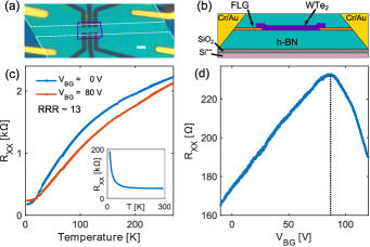
The first indication that inert atmosphere fabrication maintains crystal integrity is the temperature dependence of the resistance, shown in Fig. 1(c). We observe metallic behavior with a residual resistivity ratio (RRR) of 13. In contrast, non-encapsulated devices fabricated in air display insulating behavior (inset of Fig. 1(c)). In fact, in the literature a RRR of 13 is only achieved for samples greater than 33nm thick(Wang et al., 2015). Applying a bias to the electrostatic gate, we capacitively modulate the carrier density in the sample, finding that the low-temperature resistivity increases linearly with until V, beyond which the resistivity drops sharply (see Fig. 1(d))(coo, ). The noted metallic temperature dependence with RRR of order 10 is observed for all gate voltages, with two representative gate voltages shown in Fig. 1(c).
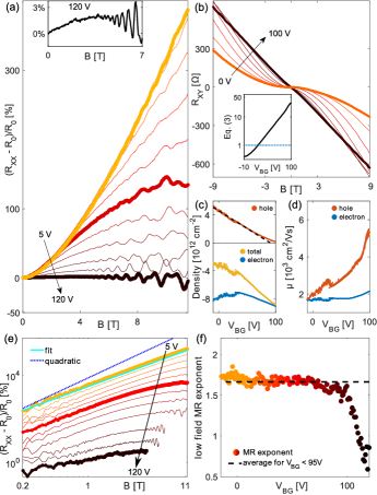
We then measure both the longitudinal () and transverse () resistances as a function of magnetic field and gate voltage in order to investigate the magnetoresistance behavior at different total carrier densities. Both measurements are shown in Fig. 2(a-b) for a range of gate voltages, where in Fig 2(a) we plot the magnetoresistance ratio (MR), defined as (coo, ). The MR shows a clear transition from strong, superlinear behavior near zero gate voltage ( increase at 11.5T) to suppressed MR () at the highest gate voltage (inset of Fig. 2(a)). During the crossover at intermediate gate voltages, we find that saturates at large , as expected for a non-compensated semimetal (Du et al., 2005; Alers and Webber, 1953). Importantly, we observe that this crossover coincides with the Hall effect transitioning from nonlinear to linear magnetic field dependence, indicating a transition from two carrier types to a single carrier type.
To investigate this behavior in more detail, we employ the semiclassical two-carrier model, which gives the following equations for the longitudinal and transverse resistivity of a semimetal:
| (1) | |||||
| (2) |
which include the electron charge and four free parameters: the density (, ) and mobility () of each carrier type, where and refer to electron-like and hole-like carriers, respectively. We fit and simultaneously to extract all four quantities at each gate voltage. (Here we constrain the electron density based on the SdH analysis presented below, but the important qualitative behavior doesn’t require this. See SI for the details(SI, ).) The fit parameters are plotted as a function of in Fig. 2(c-d). Most notably, we find that the hole density decreases monotonically to nearly zero at , consistent with our earlier, qualitative interpretation of the data.
We highlight now a particular aspect of the semiclassical model regarding the onset of saturation (or absence thereof). The condition for onset of significant saturation in the MR is given by the ratio of the two terms in the denominator of equation (1):
| (3) |
which is plotted in the inset to Fig. 2(b) for . This condition is satisfied for , around which gate voltage we see the onset of saturation in the MR. The ratio is greater than 10 for for which gate voltages we observe near complete saturation at high magnetic field. When seemingly unsaturating MR is observed in a semimetal, equation (3) can set a bound for the degree of non-compensation. For example, Ali, et al, (Ali et al., 2014) measure effectively no saturation in bulk WTe2 in fields up to 60T. From this and the mobility (which sets the magnitude of the MR), one may estimate an upper bound for the relative carrier density difference , which is an order of magnitude smaller than that estimated from SdH measurements of the bulk Fermi surface(Zhu et al., 2015; Rhodes et al., 2015). This suggests that other factors may be involved in avoiding saturation at the highest fields for 3D samples (Wang et al., 2016). A possible avenue would be to investigate the role of mobility anisotropies, known to be important in bismuth(Collaudin et al., 2015). Nonetheless, for the range of magnetic fields studied here, our analysis confirms that the large MR observed in WTe2 is rooted in the near-compensation of electron and hole densities.
Upon closer examination of our data, we find that the MR is actually sub-quadratic111While the non-parabolicity of the low-field MR may introduce a systematic error to the fits by the semiclassical MR equations, it does not change the qualitative behavior of the fit parameters nor our general conclusions – similar behavior is observed when fitting the Hall data with a constraint given only by the zero-field longitudinal resistance (see SI for details(SI, )). Lacking a physical model for the modified power law, we choose not to artificially alter the two-carrier model for the fits.. We can see this clearly by looking at the data in log-log format, as shown in Figure 2(e). An explicit fit of the power law gives an exponent near , which is consistent for sample A in two different cooldowns as well as for additional devices presented in the supplement(SI, ). The exponent is stable for nearly all gate voltages for all devices, except above for sample A, beyond which the exponent drops rapidly (Fig. 2(f)). This drop-off coincides with the indications of depletion of the holes, reinforcing that the MR can be understood as that of a standard semimetal with a correction to the exponent.
The origin of the correction to the exponent is as yet unclear. Many studies on bulk WTe2 have noted a large, quadratic MR (Ali et al., 2014; Wu et al., 2015; Rhodes et al., 2015; Zhu et al., 2015; Wang et al., 2015; wang_direct_2016, ; Cai et al., 2015), but some that explicitly fit the power law also find sub-quadratic exponents thoutam_temp_2015 ; Wang et al. (2016). While we observe a similar deviation, our sample is in the 2D limit, whereas the Fermi surface of bulk WTe2 is 3D in character(Zhu et al., 2015; Rhodes et al., 2015), suggesting that dimensionality is not a driving factor. Additionally, we find that the power law is density-independent in the semimetallic regime, and almost no MR is observed in the electron-only regime. This suggests that the coexistence of electrons and holes is crucial. One might look to semimetallic Boltzmann transport models which predict that boundary effects can generate linear MR when the valley recombination length is comparable to the transport channel width (Babkin and Kravchenko, 1971; Alekseev et al., 2015), but this requires classically strong magnetic fields not present here ( for this work). Inter-species drag effects may also play a role in magnetoresistance (coulombdragreview, ), but finite inter-valley scattering should suppress such physics. The question of the unusual magnetoresistance poses an experimental and theoretical challenge for future investigation.
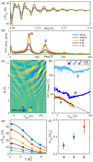
We now turn to analysis of the quantum oscillations. In Fig. 3(a) we show representative measurements of , the resistivity after subtracting a smooth quadratic background above 2 T, in the electron-only regime (). At this gate voltage, two oscillations are clearly visible, confirmed by the two peaks visible in the Fourier transform of the data in Fig. 3(b), which we label and . In Fig. 3(c) we show a map of with respect to both and . A third, hole-like dispersing oscillation is additionally visible for lower gate voltages (highlighted by dotted white lines), which we label . This is made clearer by fast Fourier transform (FFT) analysis, as shown in Figure 3(d) where the three observed peak frequencies are tracked as a function of gate voltage(SI, ). The and frequencies disperse weakly with gate voltage in a very similar manner as the electron carrier density from the semiclassical analysis. The non-monotonic gate dependence of the electron bands is likely the result of strong electric field effects, which can be explored in future devices employing a dual-gate geometry(Qian et al., 2014; Taychatanapat and Jarillo-Herrero, 2010). The third oscillation frequency, , decreases monotonically with increasing gate voltage, which we can extrapolate to zero frequency (full depletion) at roughly . This depletion voltage agrees with what is found for the positive charge carriers in the semiclassical analysis, so we ascribe the pocket to a valence band. Curiously, this depletion also coincides with a peak in the amplitude of the SdH oscillations of the and pockets (see Fig. 3(c)), suggesting that scattering between the electron and hole valleys is important.
We also conduct temperature dependence of the SdH oscillations. Fitting the Lifshitz-Kosevich formula to the temperature dependence of resistance oscillation maxima allows for extraction of the effective mass. In multi-band systems care must be taken to extract the oscillation amplitude of an individual frequency, which can be done by an appropriate FFT analysis (see SI for more details (SI, )). An example fit for the pocket oscillation is shown in Fig. 3(e), giving , where is the bare electron mass. Similar analysis for the other bands give and (see Fig. 3(f))(SI, )222Fits to the temperature dependence of multiple resistance maxima at several (nearby) gate voltages are averaged to obtain the mean effective mass. At least 20 different fits are made for each Fermi pocket.. These values are somewhat smaller than those reported for bulk crystals, which range from 0.3 to 1 (Cai et al., 2015; Zhu et al., 2015). The electron effective masses are in good agreement with theory for the monolayer, while the hole mass is again smaller than that prediction by about a factor of two(Lv et al., 2015). We note that explicit predictions for few-layer WTe2 have not yet been made.
In summary, we investigated electronic transport in encapsulated, ultra-thin WTe2. We find that a strong, intrinsic MR can be turned off by electrostatically doping the sample from a semimetallic state to an electron-only regime. We confirm the basis of the two regimes by simultaneously analyzing the MR and the Hall effect with a two-carrier model as well as by analysis of Shubnikov-de Haas oscillations, both of which indicate depletion of hole-like carriers in the suppressed-MR regime. These observations confirm that the MR in WTe2 is qualitatively explained by semiclassical transport of a semimetal, with potentially new physics in a modified exponent to the MR power law.
Acknowledgements.
This work was partly supported by the DOE, Basic Energy Sciences Office, Division of Materials Sciences and Engineering, under award DE-SC0006418 (sample fabrication and measurements) and partly through AFOSR Grant No. FA9550-16-1-0382 (data analysis), as well as the Gordon and Betty Moore Foundation’s EPiQS Initiative through Grant No. GBMF4541 to P.J.H.. Device nanofabrication was partly supported by the Center for Excitonics, an Energy Frontier Research Center funded by the DOE, Basic Energy Sciences Office, under Award No. DE-SC0001088. Crystal growth at Princeton University was supported by the NSF MRSEC program grant DMR-1005438. This work made use of the Materials Research Science and Engineering Center Shared Experimental Facilities supported by NSF under award DMR-0819762. Sample fabrication was performed partly at the Harvard Center for Nanoscale Science supported by the NSF under grant no. ECS-0335765. We thank E. Navarro-Moratalla, J. D. Sanchez-Yamagishi, and L. Bretheau for discussions and Sanfeng Wu for help with crystal exfoliation.References
- Schubnikow and Haas (1930) L. Schubnikow and W. J. d. Haas, Proceedings of the Netherlands Royal Academy of Science 33, 130 (1930).
- Shoenberg (2009) D. Shoenberg, Magnetic Oscillations in Metals (Cambridge University Press, 2009).
- Goerbig (2011) M. O. Goerbig, Reviews of Modern Physics 83, 1193 (2011).
- Das Sarma et al. (2011) S. Das Sarma, S. Adam, E. H. Hwang, and E. Rossi, Reviews of Modern Physics 83, 407 (2011).
- Ali et al. (2014) M. N. Ali, J. Xiong, S. Flynn, J. Tao, Q. D. Gibson, L. M. Schoop, T. Liang, N. Haldolaarachchige, M. Hirschberger, N. P. Ong, and R. J. Cava, Nature 514, 205 (2014).
- Shekhar et al. (2015) C. Shekhar, A. K. Nayak, Y. Sun, M. Schmidt, M. Nicklas, I. Leermakers, U. Zeitler, Y. Skourski, J. Wosnitza, Z. Liu, Y. Chen, W. Schnelle, H. Borrmann, Y. Grin, C. Felser, and B. Yan, Nature Physics advance online publication (2015), 10.1038/nphys3372.
- Vafek and Vishwanath (2014) O. Vafek and A. Vishwanath, Annual Review of Condensed Matter Physics 5, 83 (2014).
- Xu et al. (2015) S.-Y. Xu, I. Belopolski, N. Alidoust, M. Neupane, G. Bian, C. Zhang, R. Sankar, G. Chang, Z. Yuan, C.-C. Lee, S.-M. Huang, H. Zheng, J. Ma, D. S. Sanchez, B. Wang, A. Bansil, F. Chou, P. P. Shibayev, H. Lin, S. Jia, and M. Z. Hasan, Science 349, 613 (2015).
- Ali et al. (2015) M. N. Ali, L. Schoop, J. Xiong, S. Flynn, Q. Gibson, M. Hirschberger, N. P. Ong, and R. J. Cava, EPL (Europhysics Letters) 110, 67002 (2015).
- Soluyanov et al. (2015) A. A. Soluyanov, D. Gresch, Z. Wang, Q. Wu, M. Troyer, X. Dai, and B. A. Bernevig, Nature 527, 495 (2015).
- Qian et al. (2014) X. Qian, J. Liu, L. Fu, and J. Li, Science 346, 1344 (2014).
- Babkin and Kravchenko (1971) G. Babkin and V. Y. Kravchenko, JETP 33, 378 (1971).
- Alekseev et al. (2015) P. S. Alekseev, A. P. Dmitriev, I. V. Gornyi, V. Y. Kachorovskii, B. N. Narozhny, M. Schütt, and M. Titov, Physical Review Letters 114, 156601 (2015).
- Zhu et al. (2015) Z. Zhu, X. Lin, J. Liu, B. Fauqué, Q. Tao, C. Yang, Y. Shi, and K. Behnia, Physical Review Letters 114, 176601 (2015).
- Pletikosić et al. (2014) I. Pletikosić, M. N. Ali, A. V. Fedorov, R. J. Cava, and T. Valla, Physical Review Letters 113, 216601 (2014).
- Wu et al. (2015) Y. Wu, N. H. Jo, M. Ochi, L. Huang, D. Mou, S. L. Bud’ko, P. C. Canfield, N. Trivedi, R. Arita, and A. Kaminski, Physical Review Letters 115, 166602 (2015).
- Jiang et al. (2015) J. Jiang, F. Tang, X. C. Pan, H. M. Liu, X. H. Niu, Y. X. Wang, D. F. Xu, H. F. Yang, B. P. Xie, F. Q. Song, P. Dudin, T. K. Kim, M. Hoesch, P. K. Das, I. Vobornik, X. G. Wan, and D. L. Feng, Physical Review Letters 115, 166601 (2015).
- Rhodes et al. (2015) D. Rhodes, S. Das, Q. R. Zhang, B. Zeng, N. R. Pradhan, N. Kikugawa, E. Manousakis, and L. Balicas, Physical Review B 92, 125152 (2015).
- Das et al. (2016) P. K. Das, D. Di Sante, I. Vobornik, J. Fujii, T. Okuda, E. Bruyer, A. Gyenis, B. E. Feldman, J. Tao, R. Ciancio, G. Rossi, M. N. Ali, S. Picozzi, A. Yadzani, G. Panaccione, and R. J. Cava, Nature Communications 7, 10847 (2016).
- Wang et al. (2016) Y. Wang, K. Wang, J. Reutt-Robey, J. Paglione, and M. S. Fuhrer, Physical Review B 93, 121108 (2016).
- Wang et al. (2015) L. Wang, I. Gutiérrez-Lezama, C. Barreteau, N. Ubrig, E. Giannini, and A. F. Morpurgo, Nature Communications 6, 8892 (2015).
- (22) Lin Wang, Ignacio Gutierrez-Lezama, Celine Barreteau, Dong-Keun Ki, Enrico Giannini, and Alberto F. Morpurgo. Physical Review Letters, 117(17):176601, October 2016.
- Lee et al. (2015) C.-H. Lee, E. C. Silva, L. Calderin, M. A. T. Nguyen, M. J. Hollander, B. Bersch, T. E. Mallouk, and J. A. Robinson, Scientific Reports 5, 10013 (2015).
- (24) Fan Ye, Jaesung Lee, Jin Hu, Zhiqiang Mao, Jiang Wei, and Philip X.-L. Feng. Small, 12(42):5802–5808, November 2016.
- (25) Zaiyao Fei, Tauno Palomaki, Sanfeng Wu, Wenjin Zhao, Xinghan Cai, Bosong Sun, Paul Nguyen, Joseph Finney, Xiaodong Xu, and David H. Cobden. arXiv:1610.07924 [cond-mat], October 2016. arXiv: 1610.07924.
- Tsen et al. (2015) A. W. Tsen, R. Hovden, D. Wang, Y. D. Kim, J. Okamoto, K. A. Spoth, Y. Liu, W. Lu, Y. Sun, J. C. Hone, L. F. Kourkoutis, P. Kim, and A. N. Pasupathy, Proceedings of the National Academy of Sciences 112, 15054 (2015).
- Dean et al. (2010) C. R. Dean, A. F. Young, I. Meric, C. Lee, L. Wang, S. Sorgenfrei, K. Watanabe, T. Taniguchi, P. Kim, K. L. Shepard, and J. Hone, Nature Nanotechnology 5, 722 (2010).
- Wang et al. (2013) L. Wang, I. Meric, P. Y. Huang, Q. Gao, Y. Gao, H. Tran, T. Taniguchi, K. Watanabe, L. M. Campos, D. A. Muller, J. Guo, P. Kim, J. Hone, K. L. Shepard, and C. R. Dean, Science 342, 614 (2013).
- Cui et al. (2015) X. Cui, G.-H. Lee, Y. D. Kim, G. Arefe, P. Y. Huang, C.-H. Lee, D. A. Chenet, X. Zhang, L. Wang, F. Ye, F. Pizzocchero, B. S. Jessen, K. Watanabe, T. Taniguchi, D. A. Muller, T. Low, P. Kim, and J. Hone, Nature Nanotechnology 10, 534 (2015).
- (30) See supplemental material at [url will be inserted by publisher] for (1) details of the two carrier analysis and fits, (2) investigation of the FLG-WTe2 contact resistance, (3) more information on the SdH oscillation analysis, and (4) additional data on other devices. .
- (31) Data in Fig. 1 are from initial measurements in a 4K probe. Data and analysis in Fig. 2(b-d) are from a second cooldown at 300 mK (more details in the supplement). All other data and analysis in the main text are from a third cooldown with base temperature of 30 mK. .
- Du et al. (2005) X. Du, S.-W. Tsai, D. L. Maslov, and A. F. Hebard, Physical Review Letters 94, 166601 (2005).
- Alers and Webber (1953) P. B. Alers and R. T. Webber, Physical Review 91, 1060 (1953).
- Collaudin et al. (2015) A. Collaudin, B. Fauqué, Y. Fuseya, W. Kang, and K. Behnia, Physical Review X 5, 021022 (2015).
- Note (1) While the non-parabolicity of the low-field MR may introduce a systematic error to the fits by the semiclassical MR equations, it does not change the qualitative behavior of the fit parameters nor our general conclusions – similar behavior is observed when fitting the Hall data with a constraint given only by the zero-field longitudinal resistance (see SI for details(SI, )). Lacking a physical model for the modified power law, we choose not to artificially alter the two-carrier model for the fits.
- Cai et al. (2015) P. L. Cai, J. Hu, L. P. He, J. Pan, X. C. Hong, Z. Zhang, J. Zhang, J. Wei, Z. Q. Mao, and S. Y. Li, Physical Review Letters 115, 057202 (2015).
- (37) L. R. Thoutam, Y.L. Wang, Z.L. Xiao, S. Das, A. Luican-Mayer, R. Divan, G.W. Crabtree, and W.K. Kwok. Physical Review Letters, 115(4):046602, July 2015.
- (38) B. N. Narozhny and A. Levchenko, Rev. Mod. Phys. 88, 25003 (2016) .
- Taychatanapat and Jarillo-Herrero (2010) T. Taychatanapat and P. Jarillo-Herrero, Physical Review Letters 105, 166601 (2010).
- Note (2) At least 20 different fits to the temperature dependence of resistance maxima at several gate voltages are averaged to obtain the mean effective mass.
- Lv et al. (2015) H. Y. Lv, W. J. Lu, D. F. Shao, Y. Liu, S. G. Tan, and Y. P. Sun, EPL (Europhysics Letters) 110, 37004 (2015).