Tuning the p-type Schottky barrier in 2D metal/semiconductor interface: boron-sheet/MoSe2, and /WSe2
Abstract
The electronic and the structural properties of two dimensional van der Waals metal/semiconductor heterostructures have been investigated through first-principles calculations. We have considered the recently synthesized borophene [Science 350, 1513 (2015)], and the planar boron sheets (S1 and S2) [Nature Chemistry 8, 563 (2016)] as the 2D metal layer, and the transition metal dichalcogenides (TMDCs) MoSe2, and WSe2 as the semiconductor monolayer. We find that the energetic stability of those 2D metal/semiconductor heterojunctions is mostly ruled by the vdW interactions; however, chemical interactions also take place in borophene/TMDC. The electronic charge transfers at the metal/semiconductor interface has been mapped, where we find a a net charge transfer from the TMDCs to the boron sheets. Further electronic structure calculations reveal that the metal/semiconductor interfaces, composed by planar boron sheets S1 and S2, present a p-type Schottky barrier which can be tuned to a p-type ohmic contact upon an external electric field.
pacs:
.I Introduction
Two dimensional (2D) systems have been the subject of numerous studies addressing not only the fundamental research but also technological applications focusing the development of electronic devices. Such a 2D scenario in the material science was predicted by Geim and Grigorieva Geim and Grigorieva (2013), where they present the concept of van der Waals (vdW) heterostructures, and more recently by Novoselov et al. Novoselov et al. (2016). Here, the electronic properties of those vdW heterostructures can be tuned by stacking different sets of layered, semiconductor or metallic, materials.
Since the successful synthesis of single layer MoS2 transistor Radisavljevic et al. (2011), transition metal dichalcogenides (TMDCs) have been considered quite promising to be used in 2D vdW heterostructures. For instance, semiconductor/semiconductor vdW heterojunction composed by layered MoSe2/WSe2 Huang et al. (2014), and MoS2/WS2 Gong et al. (2014). Here a formidable bandgap engineering can be done through a suitable choice of the stacked 2D materials, as well as the number of the stacked layers. Based on first-principles calculations, Kang et al. Kang et al. (2013) performed an extensive study of the band offsets of TMDCs. The band offsets were estimated by comparing the ionization potentials and the band gaps of the stacked 2D components, showing that MoSe2/WSe2, MoS2/WS2 and MoS2/WSe2 heterojunctions present type-II band alignment. Indeed, such a type-II band offset was verified in a recent experimental realization of MoS2/WSe2 p-n heterojunction Lee et al. (2014). Meanwhile, metal/semiconductor 2D vdW heterostructures have been successfully synthesized through deposition of 2D (semi)metal on layered TMDC, for instance, graphene on TMDCs Yu et al. (2014); Shih et al. (2014), or 2D metallic TMDCs, like H-NbS2, on semiconductor TMDCs Liu et al. (2016a).
In vdW heterostructures, the Schottky barrier () can be estimated by comparing the work function of the metal and the electronic affinity (n-type ) or the ionization potential (p-type ) of the semiconductor. Similarly to their 3D counterpart, the height of the Schottky barrier can be tuned by an external electric field, as observed in field effect transistors (FETs). However, the hole injection in FETs based on (semiconductor) TMDC has been limited by the larger values of the p-type . There are some of proposals aiming to provide an efficient hole injection in TMDCs; for instance, by using the oxidized graphene at the source/drain contacts Chuang et al. (2014); Musso et al. (2014), and more recently the inclusion of a BN monolayer at the metal/semiconductor interface Farmanbar and Brocks (2015). However, the control of the p-type , in order to get an efficient hole injection in the metal/TMDCs heterojunctions, is still a challenge. Fortunately, nowadays we are facing an intense research on the new materials, including 2D crystals, allowing to make a number of material combinations focusing on a given electronic property; for instance the p-type Schottky barrier in metal/semiconductor-TMDCs.
Very recently metallic 2D boron sheets lying on the Ag(111) surface have been successfully synthesized, where one is characterized by vertically buckled boron atoms, hereafter named S0 [Fig. 1(a1)] Mannix et al. (2015). While the others, upon the presence of boron vacancies, are flat [S1 and S2 in Figs. 1(b1) and (c1)] Feng et al. (2016). Here one can guess that those 2D boron sheets may act as the metal contact in 2D vdW heterostructures. In a recent theoretical study Alvarez-Quiceno et al. (2017), supported by the experimental findings Mannix et al. (2015), the authors verified that the oxidation of S0 is quite likely, giving rise to boron vacancies, which somewhat mimic the planar geometries of S1 and S2, as verified by Feng et al. Feng et al. (2016). Beside the inertness with respect to the oxidation process, it has been reported that the boron sheets S1 and S2 are energetically more stable than the buckled geometry of borophene, S0.
In this work, based on the first-principles calculations, we investigate the energetic stability and the electronic properties of 2D metal/semiconductor heterojunctions. We have considered the recently synthesized boron sheets S0–S2 Mannix et al. (2015); Feng et al. (2016) as the 2D metallic layer; and monolayers (MLs) of TMDCs MoSe2 and WSe2 as the semiconductor system. Our total energy results show that the energetic stability of those metal/semiconductor interfaces is mostly dictated by the vdW interactions. Further electronic band structure calculations reveal the formation of interface (metallic) states in S0/TMDC, pinning the Fermi level within the energy gap of the TMDC. On the other hand, S1/ and S2/TMDC heterojunctions present a tunable p-type Schottky barrier; where we show that the former system presents a p-type ohmic contact upon an external electric field smaller than 4 V/nm.
II Method
The calculations were performed using the density functional theory (DFT) as implemented in the VASP code Kresse and Furthmller (1996a, b). The exchange-correlation potential was described within the generalized gradient approximation (GGA-PBE) Perdew et al. (1996), and the electron-ion interactions were treated by using the the projected augmented wave approach (PAW) Blchl (1994); Kresse and Joubert (1999). The Kohn-Sham wave functions were expanded in a plane-wave basis set with an energy cutoff of 400 eV. The atomic positions were fully relaxed by including the van der Waals interactions by using the self-consistent opt88vdW approach Dion et al. (2004); Klimeš et al. (2009). We have considered a force convergence tolerance of 20 meV/Å. In order to verify the validity of our results, the electronic structure of the pristine systems, viz.: single layer MoSe2, WSe2, and the boron sheets S0–S2 were calculated using HSE06 hybrid functional Heyd et al. (2006). The metal/semiconductor interfaces were described within the slab method, where we have introduced a vacuum region of 15 Å, perpendicular to the metal/semiconductor interface, in order to prevent spurious interactions between a given interface and its (periodic) image. The Brillouin zone sampling was performed by using a set of 12121 k-points within the Monkhorst-Pack scheme Monkhorst and Pack (1976).
III Results
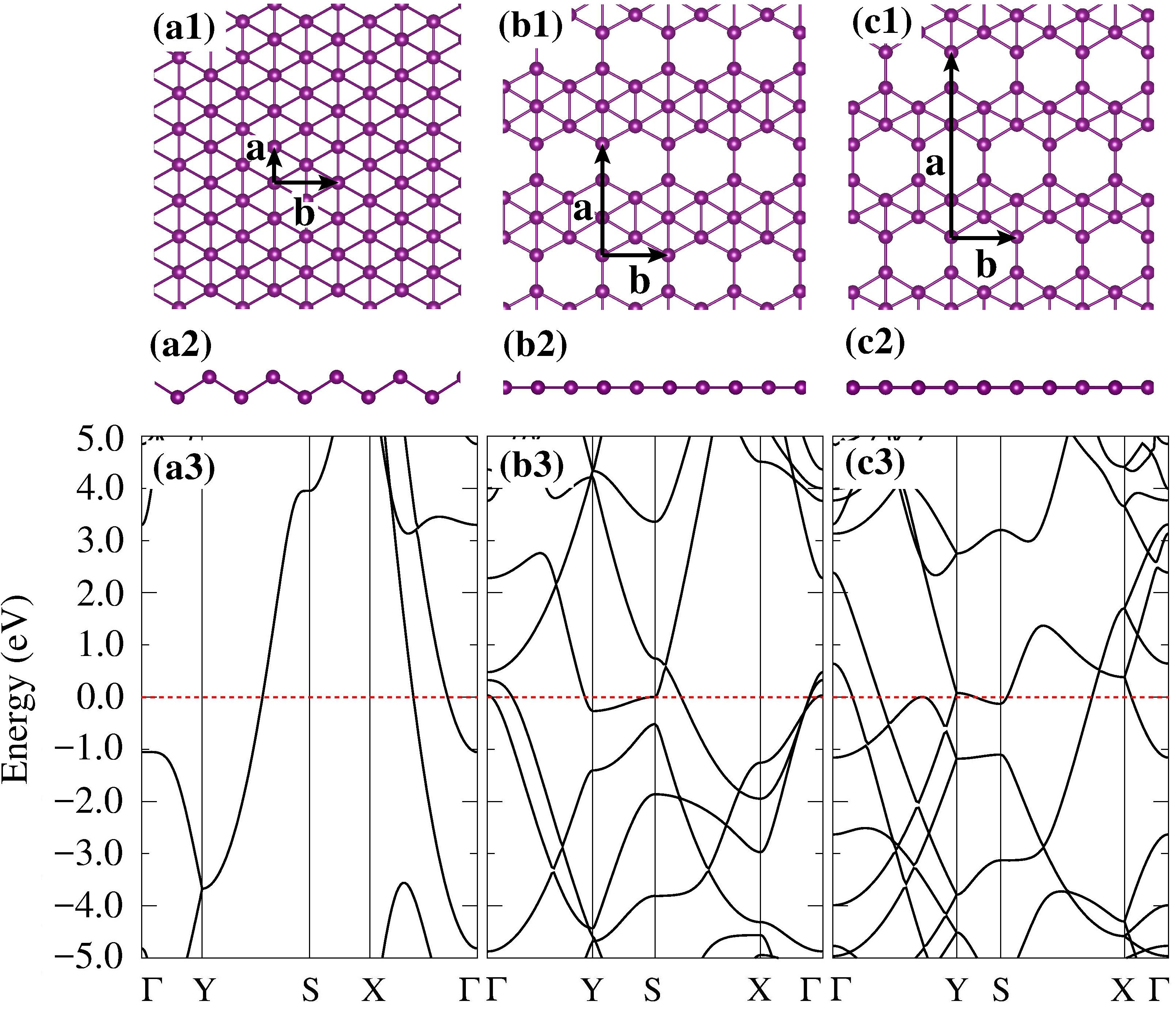
In Fig. 1 we present the structural models and the electronic band structures of pristine free-standing boron sheets S0–S2, Figs. 1(a)–(c). In agreement with the recent experimental findings, boron atoms in S0 [Fig. 1(a1)] present a vertical buckling of 0.91 Å, giving rise to boron stripes along the direction. Meanwhile, upon the formation of boron vacancies, the structural models S1 and S2 become planar, Fig. 1(b1) and (b2). The electronic band structure of S0, Fig. 1(a3), presents a set of metallic bands for wave vectors parallel to the direction, that is along the boron stripes; whereas there are no metallic bands for wave vectors along the Y abd SX directions. Such a band structure anisotropy is reduced in S1 and S2, Figs. 1(b3) and (c3). The energy bands of boron sheets S1 and S2 are characterized by the formation of dispersionless metallic bands along the YS, and higher density of states (DOS) near the Fermi level (), when compared with the DOS of S0. In a previous work, we find that the anisotropy of the energy bands in borophene promotes a peculiar directional dependence of its electronic transport properties Padilha et al. (2016). Here we will examine how those energy bands change upon the formation of 2D metal/semiconductor heterostructures, and their role on the Schottky barrier.
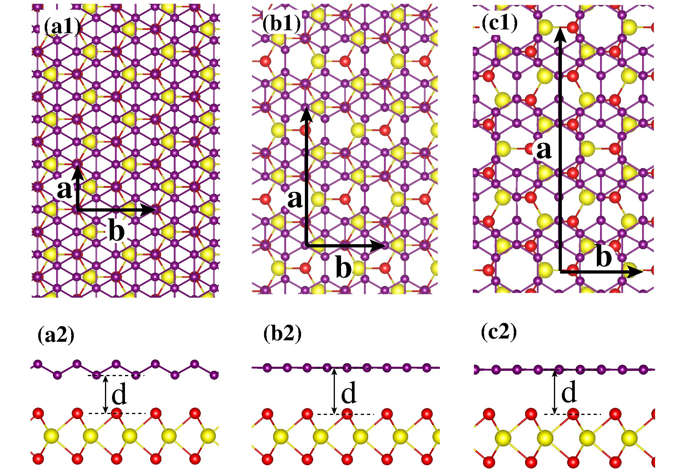
In Fig. 2 we present the structural models of metal/semiconductor systems (semiconductor = TMDCs MoSe2 and WSe2 monolayers), for metal = S0 (a), S1 (b), and S2 (c). In order to minimize the lattice mismatch between the boron sheets and the TMDC monolayers, the former were described by orthorhombic supercells with surface periodicities of (22). In this case, the boron sheets are strained by up to % with respect to their equilibrium lattice constant. For the MoSe2 and WSe2 monolayers (MLs) we have considered orthorhombic unit cells with the following surface periodicities, (11), (31), and (51) for S0/MoSe2 (S0/WSe2), S1/MoSe2 (S1/WSe2), and S2/MoSe2 (S2/WSe2), respectively. In this case, the MoSe2 and WSe2 monolayers are strained by up to %, when compared with their equilibrium lattice constant.
The energetic stability of 2D heterostructures was inferred through the calculation of the metal/TMDC binding energy (), defined as,
where and represent the total energies of the separated systems, boron sheets and the TMDCs; and is the total energy of the final system, metal/TMDC 2D heterojunction. We have considered four different metal/TMDC interface configurations, where we found between 34 and 44 meV/Å2 for S0/MoSe2, and meV/Å2 for S0/WSe2. At the equilibrium geometry, the borophene sheet S0 and MoSe2 (WSe2) monolayer presents a vertical distance () between 2.79 (2.90) and 3.17 Å (3.55 Å). Those findings of and are somewhat comparable with the ones obtained for bilayer-graphene on the Cu(111) surface Souza et al. (2016), namely of about 39 meV/Å2, and vertical distance of 2.9 Å; which allow us to infer that the energetic stability of borophene/TMDC systems is mostly dictated by vdW interactions. Indeed, by turning off the vdW contribution, we obtained of 0.13 meV/Å2 and =3.97 Å. However, as will be discussed below, the chemical interaction between S0 and the TMDC can not be neglected for Å. The binding energy reduces for the planar boron sheets S1 and S2, namely we obtained =33 and 31 meV/Å2 for S1/ and S2/MoSe2 respectively, and Å. Our results of binding energies and equilibrium geometries, for the energetically most stable configurations, are summarized in Table I.
| metal/semic. | ||
|---|---|---|
| S0/MoSe2 | 44 | 2.79 |
| S0/WSe2 | 41 | 2.90 |
| S1/MoSe2 | 33 | 3.33 |
| S1/WSe2 | 31 | 3.23 |
| S2/MoSe2 | 31 | 3.36 |
| S2/WSe2 | 30 | 3.39 |

Upon the formation of metal/TMDC heterostructures, there is a net charge transfer () at the metal/TMDC interface region. We may have a spacial picture of by comparing the total charge densities of the final system () with the ones of the (initial) separated components, metallic boron sheet () and semiconductor MoSe2 and WSe2 (),
In Figs. 3(a) and (b) we present our result of for S0/MoSe2 and S0/WSe2, where we verify that the interface region near the Se layer presents a charge density loss (), whereas near the borophene layer we find (mostly) . Based on the Bader charge density analysis Bader (1990), we find that the total charge density of the MoSe2 and WSe2 monolayer reduces by 0.75 and e/cm2. That is, indeed there is a net charge transfer from the boron sheet S0 to the MoSe2 and WSe2 MLs.
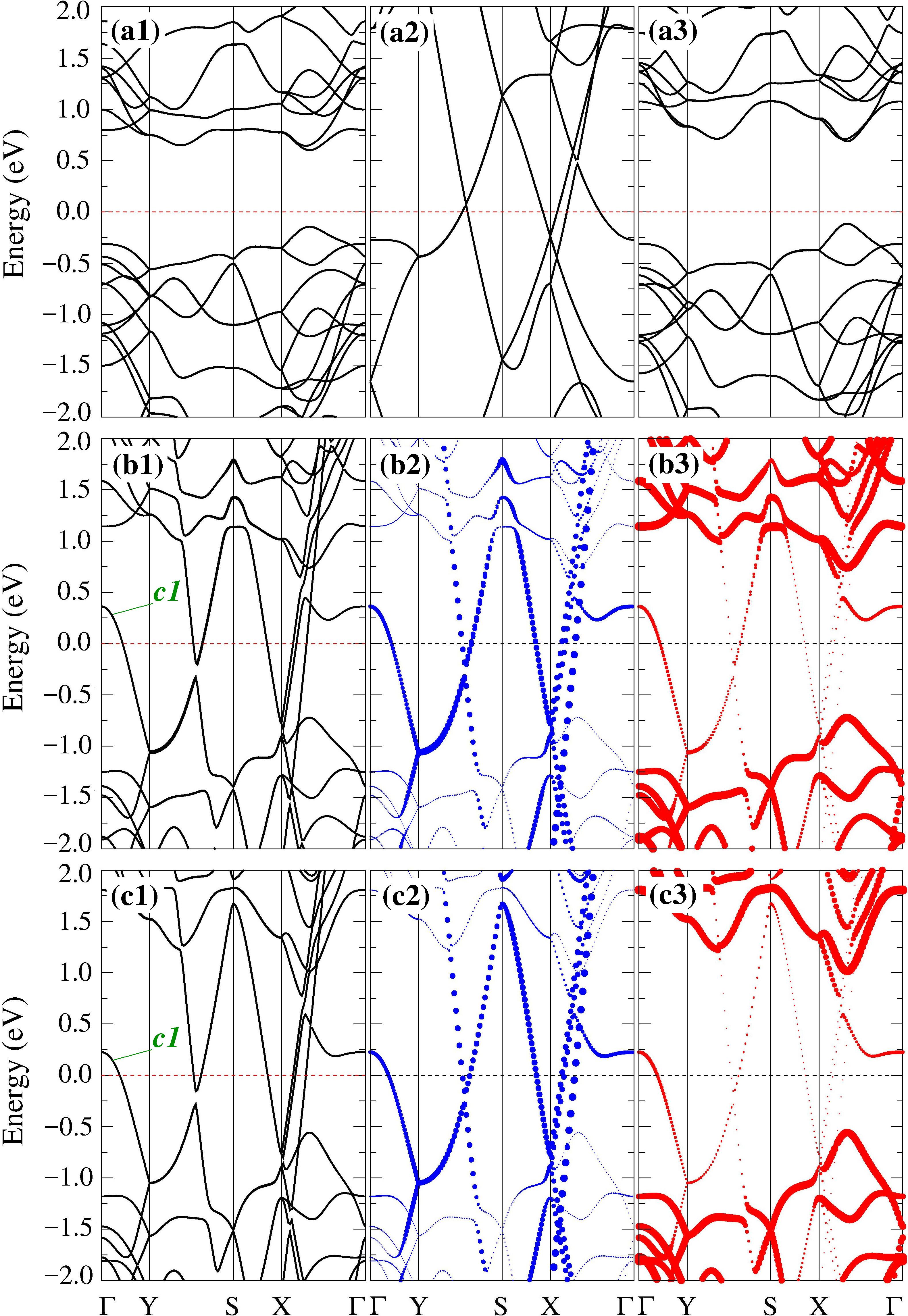
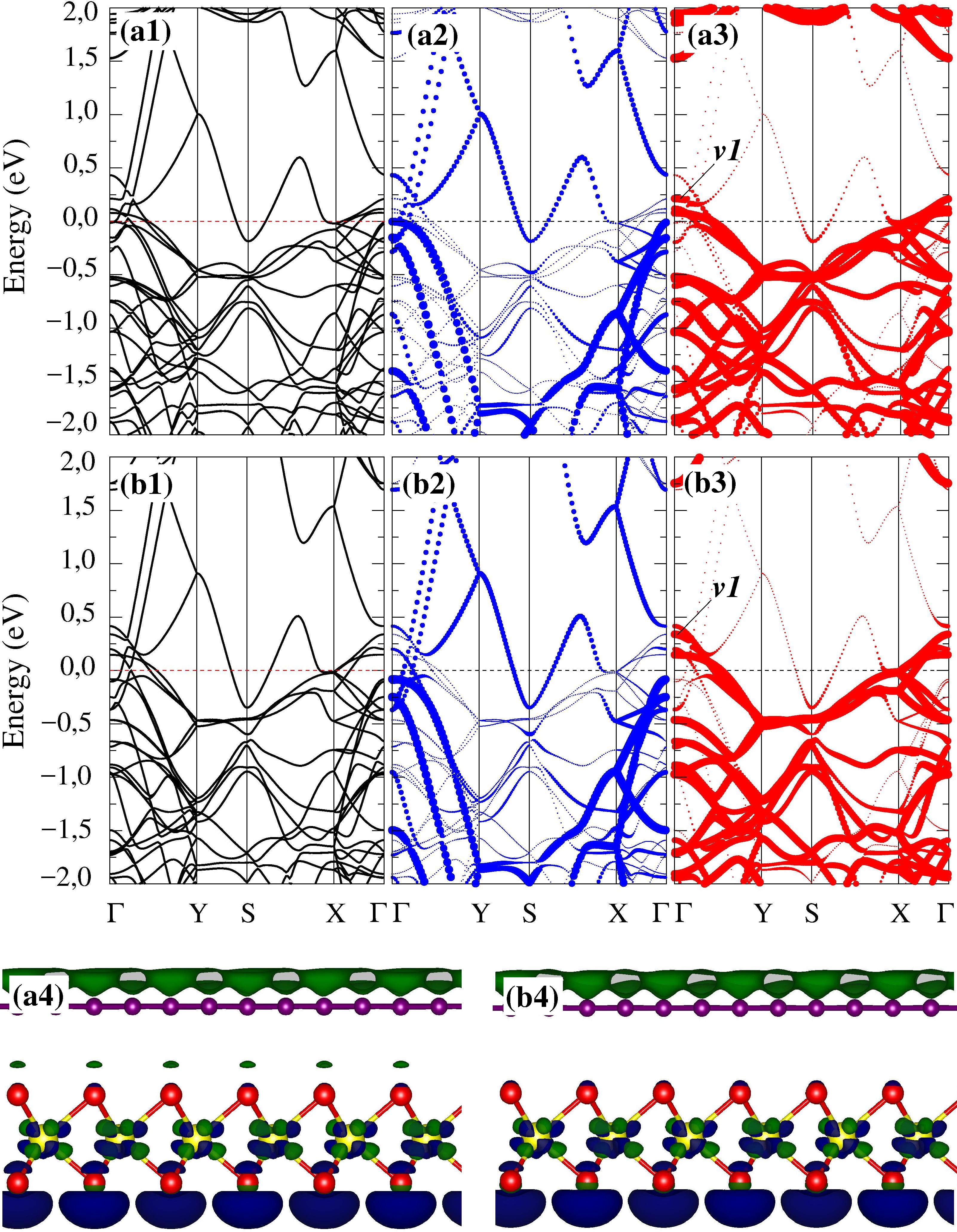
Figures 4(a1)–(a3) show the electronic band structures of the pristine systems considering the (11) orthorhombic unit cells for MoSe2 and WSe2, and (22) for the boron sheet S0, confirming the semiconductor (metallic) character of MoSe2 and WSe2 (S0). In Figs. 4(b1) and (c1) we present the electronic band structure of S0/MoSe2 and S0/WSe2. The projection of the energy bands on S0 [Figs. 4(b2) and (c2)] reveals that its metallic bands exhibit a downshift in energy with respect to the Fermi level (). This is in agreement with the semiconductor S0 net charge transfers. In addition, we find the formation of a metallic band for wave vectors parallel to the Y direction. Further projected energy bands, Figs. 4(b3) and (c3), show that the MoSe2 and WSe2 MLs also contribute to the formation of . Thus, indicating that the metallic interface states comes from the hybridization between the electronic states of the boron sheet S0 and the TMDCs. In order to provide further support to the statement above, we have performed additional electronic band structure calculations by increasing the interlayer distance [Fig. 2(a2)]. We find that for about 4 Å the electronic contributions from the MoSe2 and WSe2 MLs to become negligible; it becomes fully occupied and localized on the borophene layer. That is, the metallic interface states in S0/TMDC are suppressed by increasing the vertical distance, Å.
Our results of for S1 and S2 lying on the MoSe2 and WSe2 MLs are lower when compared with S0/MoSe2 and S0/WSe2; in addition, the interlayer separation increases to Å, Table I. Those findings indicate that the electronic interaction between the boron sheets (S1 and S2) and the semiconductor MoSe2 and WSe2 MLs are weaker compared to the S0/TMDC systems. Indeed, this is what we find in Fig. 5, where we can see that the energy bands of the separated components are mostly preserved. Based on the Schottky-Mott approach, we find that the MoSe2 and WSe2 MLs on S1 present a p-type Schottky barrier. Here is given by the energy difference between the VBM of the semiconductor ML and the Fermi level () of the metal/semiconductor-TMDC heterostructure, . For instance, we find a p-type Schottky barrier of 0.15 eV in S1/MoSe2, while it reduces to eV in S1/WSe2. It is worth noting that, although the structural and energetic similarities with the S1/TMDC, the S2/MoSe2, and S2/WSe2 interfaces present larger values of Schottky barrier, viz.: 0.44 and 0.31 eV.
The control of the Schottky barrier through an external field, somewhat mimicking the gate electrical field, has been explored in other metal/semiconductor 2D systems Padilha et al. (2015); Liu et al. (2016b). Here, based on the same approach, we examine the dependence between and an external electric field perpendicular to the metal/TMDC interface (). Here we find that increases for pointing from the TMDC ML toward the boron sheet (i.e. positive values of ). While for negative values of , the Schottky barrier reduces, becoming negative for V/nm in S1/MoSe2 and S1/WSe2, giving rise to p-type ohmic contacts. Those results of as a function of are summarized in Table II. It is worth noting that, by increasing the strength of , the other S2/MoSe2 and S2/WSe2 systems will also present p-type ohmic contacts. On the other hand, in contrast with the Ref. Liu et al. (2016b), we did not find any significative change of as a function of ; which can be attributed to the presence of metallic interface states pinning the Fermi level in S0/TMDC.
| metal/semic. | |||
|---|---|---|---|
| S1/MoSe2 | +0.41 | +0.15 | 0.21 |
| S1/WSe2 | +0.32 | +0.01 | 0.34 |
| S2/MoSe2 | +0.70 | +0.44 | +0.29 |
| S2/WSe2 | +0.60 | +0.31 | +0.10 |
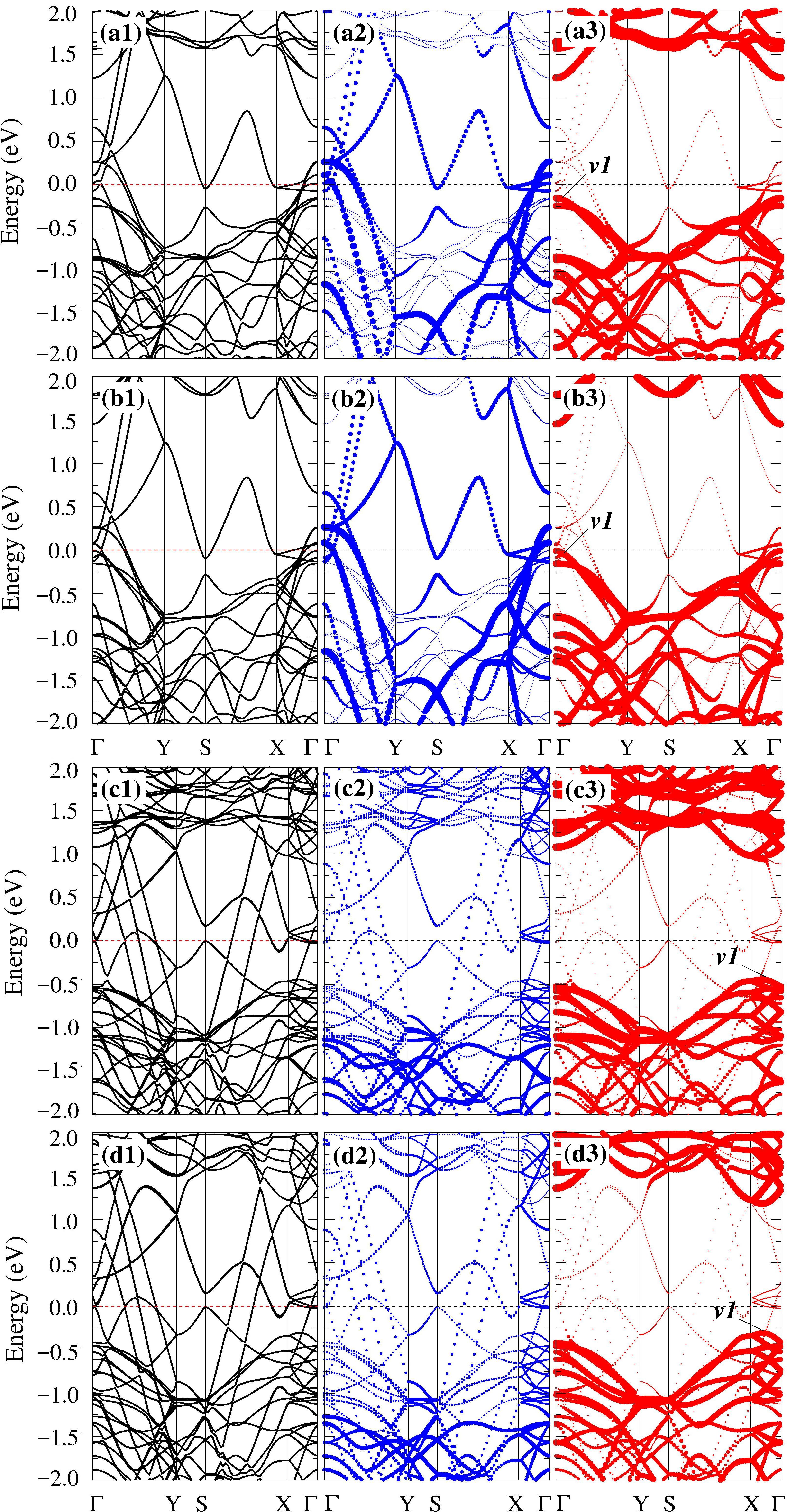
The p-type ohmic contact in S1/MoSe2 and S1/WSe2/ is characterized by net charge transfer from the TMDC layer to S1. Indeed, we find a net charge transfers from the MoSe2, and WSe2 MLs to S1 of 7.2 and e/cm2, respectively. In Figs. 6(a1)–(a3) and (b1)–(b3) we present the electronic band structure of S1/MoSe2 and S1/WSe2 upon an external field of V/nm. The projected energy bands on the boron sheet S1 [Fig. 6(a2)] and MoSe2 ML [Fig. 6(a3)] show that (i) the metallic bands of S1 are preserved , however, near the Fermi level, they present a downshift when compared with the ones at [Fig. 5(a2)]; while (ii) the energy bands projected on the MoSe2 is characterized by the formation of partially occupied states near the -point. Those findings [(i) and (ii)] reveal that, indeed, the S1/MoSe2 interface interface exhibits a p-type ohmic contact which is tuneable by an external electric field, . The same scenario has been verified for the S1/WSe2 interface. In Figs. 6(a4) and (b4), we present the charge density redistribution at the S1/MoSe2 and S1/WSe2 interfaces, respectively, as a function of the external field, namely . For both S1/TMDC systems, we find mostly localized on the Se layer opposite to the interface region; while the boron-sheet S1 presents , giving rise to a net charge density depletion at the S1/TMDC interface region.
IV Conclusions
Based on the first-principles calculations we have investigated the energetic stability and the electronic properties of 2D metal/TMDC vdW heterojunctions. We find that the recently synthesized planar boron sheets (S1 and S2) are good candidates to form p-type Schottky contacts with the TMDCs (MoSe2 and WSe2), viz.: S1/MoSe2, /WSe2, and S2/MoSe2, and /WSe2. There is a net charge transfer from the TMDCs to the boron sheets. Upon further application of external electric field, we verify that the S1/MoSe2 and /WSe2 heterojunctions exhibit a p-type ohmic contact for about 4 V/nm (absolute value). Similar results are expected for S2/MoSe2 and /WSe2, however for larger values of . In contrast, such a Schottky barrier tuning has not been verified for borophene/TMDCs, S0/MoSe2 and S0/WSe2. Instead we find the formation of metallic interface states, pining the Fermi level within the bandgap of the TMDCs.
V Acknowledgements
We would like to thank the Brazilian funding agencies CNPq, CAPES, FAPEMIG, and FAPESP. Part of calculations were performed using the computational facilities of CENAPAD/SP.
VI Appendix
Since the chemical interactions at the metal/semiconductor interface region are negligible, the Schottky-Mott model is quite suitable to estimated the Schottky barrier () in vdW metal/semiconductor heterojunctions. Within such an approach, the p-type Schottky barrier can be written as,
| (1) |
where is the ionization potential of the semiconductor, and represents the metal work function. That is, the Schottky barrier has been estimated by comparing the intrinsic properties of the isolated components.
In order to check the validity of our findings, regarding the formation of p-type Schottky barrier in the boron metal/semiconductor heterojunctions studied in the present work, we have performed additional electronic structure calculations of using the HSE06 hybrid functionals.
| Functional | MoSe2 | WSe2 | S0 | S1 | S2 |
|---|---|---|---|---|---|
| PBE-GGA | 5.32 | 5.09 | 5.28 | 4.94 | 4.78 |
| HSE06 | 5.53 | 5.30 | 5.38 | 4.95 | 4.79 |
Our PBE-GGA results of the ionization potential, Table III, are in good agreement with those obtained by Liu et al. Liu et al. (2016a), while calculated using the hybrid functionals (HSE06) increases by about 0.20 eV. In this case, we find that, within the HSE06 approach, the p-type Schottky barrier [eq. (1)] of S1/MoSe2 (S1/WSe2) increases from 0.38 to 0.58 eV (0.15 to 0.35 eV), similarly increases by about 0.2 eV in S2/MoSe2 and S2/WSe2.
References
- Geim and Grigorieva (2013) A. K. Geim and I. V. Grigorieva, Nature 499, 419 (2013).
- Novoselov et al. (2016) K. Novoselov, A. Mishchenko, A. Carvalho, and A. C. Neto, Science 353, aac9439 (2016).
- Radisavljevic et al. (2011) B. Radisavljevic, A. Radenovic, J. Brivio, i. V. Giacometti, and A. Kis, Nature nanotechnology 6, 147 (2011).
- Huang et al. (2014) C. Huang, S. Wu, A. M. Sanchez, J. J. Peters, R. Beanland, J. S. Ross, P. Rivera, W. Yao, D. H. Cobden, and X. Xu, Nature materials 13, 1096 (2014).
- Gong et al. (2014) Y. Gong, J. Lin, X. Wang, G. Shi, S. Lei, Z. Lin, X. Zou, G. Ye, R. Vajtai, B. I. Yakobson, et al., Nature materials 13, 1135 (2014).
- Kang et al. (2013) J. Kang, S. Tongay, J. Zhou, J. Li, and J. Wu, Appl. Phys. Lett. 102, 012111 (2013).
- Lee et al. (2014) C.-H. Lee, G.-H. Lee, A. M. Van Der Zande, W. Chen, Y. Li, M. Han, X. Cui, G. Arefe, C. Nuckolls, T. F. Heinz, et al., Nature nanotechnology 9, 676 (2014).
- Yu et al. (2014) L. Yu, Y.-H. Lee, X. Ling, E. J. Santos, Y. C. Shin, Y. Lin, M. Dubey, E. Kaxiras, J. Kong, H. Wang, et al., Nano letters 14, 3055 (2014).
- Shih et al. (2014) C.-J. Shih, Q. H. Wang, Y. Son, Z. Jin, D. Blankschtein, and M. S. Strano, ACS nano 8, 5790 (2014).
- Liu et al. (2016a) Y. Liu, P. Stradins, and S.-H. Wei, Science advances 2, e1600069 (2016a).
- Chuang et al. (2014) S. Chuang, C. Battaglia, A. Azcatl, S. McDonnell, J. S. Kang, X. Yin, M. Tosun, R. Kapadia, H. Fang, R. M. Wallace, et al., Nano letters 14, 1337 (2014).
- Musso et al. (2014) T. Musso, P. V. Kumar, A. S. Foster, and J. C. Grossman, ACS nano 8, 11432 (2014).
- Farmanbar and Brocks (2015) M. Farmanbar and G. Brocks, Physical Review B 91, 161304 (2015).
- Mannix et al. (2015) A. J. Mannix, X.-F. Zhou, B. Kiraly, J. D. Wood, D. Alducin, B. D. Myers, X. Liu, B. L. Fisher, U. Santiago, J. R. Guest, et al., Science 350, 1513 (2015).
- Feng et al. (2016) B. Feng, J. Zhang, Q. Zhong, W. Li, S. Li, H. Li, P. Cheng, S. Meng, L. Chen, and K. Wu, Nature chemistry 8, 563 (2016).
- Liu et al. (2016b) L. Liu, S. Xiong, and X. Wu, Applied Physics Letters 109, 061601 (2016b).
- Alvarez-Quiceno et al. (2017) J. C. Alvarez-Quiceno, R. H. Miwa, G. M. Dalpian, and A. Fazzio, 2D Materials (to be published xxx, xxx (2017).
- Kresse and Furthmller (1996a) G. Kresse and J. Furthmller, Comput. Mater. Sci. 6, 15 (1996a).
- Kresse and Furthmller (1996b) G. Kresse and J. Furthmller, Phys. Rev. B 54, 11169 (1996b).
- Perdew et al. (1996) J. P. Perdew, K. Burke, and M. Ernzerhof, Phys. Rev. Lett. 77, 3865 (1996).
- Blchl (1994) P. E. Blchl, Phys. Rev. B 50, 17953 (1994).
- Kresse and Joubert (1999) G. Kresse and D. Joubert, Phys. Rev. B 59, 1759 (1999).
- Dion et al. (2004) M. Dion, H. Rydberg, E. Schrder, D. C. Langreth, , and B. I. Lundqvist, Phys. Rev. Lett. 92, 246401 (2004).
- Klimeš et al. (2009) J. Klimeš, D. R. Bowler, and A. Michaelides, Journal of Physics: Condensed Matter 22, 022201 (2009).
- Heyd et al. (2006) J. Heyd, G. E. Scuseria, and M.Ernzerhof, J. Chem. Phys. 124, 219906 (2006).
- Monkhorst and Pack (1976) H. J. Monkhorst and J. D. Pack, Phys. Rev. B 13, 5188 (1976).
- Padilha et al. (2016) J. E. Padilha, R. H. Miwa, and A. Fazzio, Physical Chemistry Chemical Physics 18, 25491 (2016).
- Souza et al. (2016) E. S. Souza, W. L. Scopel, and R. Miwa, Physical Review B 93, 235308 (2016).
- Bader (1990) R. Bader, Atoms in Molecules: A Quantum Theory (Oxford University Press, New York, 1990).
- Padilha et al. (2015) J. Padilha, A. Fazzio, and A. J. da Silva, Physical review letters 114, 066803 (2015).