Method for determining optimal supercell representation of interfaces
Abstract
The geometry and structure of an interface ultimately determines the behavior of devices at the nanoscale. We present a generic method to determine the possible lattice matches between two arbitrary surfaces and to calculate the strain of the corresponding matched interface. We apply this method to explore two relevant classes of interfaces for which accurate structural measurements of the interface are available: (i) the interface between pentacene crystals and the (111) surface of gold, and (ii) the interface between the semiconductor indium-arsenide and aluminum. For both systems, we demonstrate that the presented method predicts interface geometries in good agreement with those measured experimentally, which present nontrivial matching characteristics and would be difficult to guess without relying on automated structure-searching methods.
I Introduction
As electronic devices shrink in size to reach nanoscale dimensions, interfaces between different materials become increasingly important in defining the device characteristics(Blom and Stokbro, 2013). In many cases, it has been shown that the effect of the interface even dominates the device propertiesDusastre et al. (2012), leading to the concept that “the interface is the device” (Kroemer, 2001). In order to optimize the performance of a device it is therefore important to understand the properties of its interfaces.
First principles modeling based on atomistic methods such as Density Functional Theory (DFT) (Martin, 2004) have become an important tool for simulating the properties of interfaces (Stradi et al., 2016). To be truly predictive, atomistic methods require an accurate model for the atomic-scale geometry of the interface. As these simulations typically use periodic boundary conditions in the direction parallel to the interface, a common supercell for the surfaces of the two crystals forming the interface must be determined. However, typically the two crystals are not commensurate and finding a common supercell requires straining one of or both the surfaces. To accommodate the resulting strain, the two surfaces can also be rotated with respect to each other. However, for rotation angles preserving a high symmetry in the supercell, this has often the side-effect of increasing considerably its dimensions. Finding a supercell with low built-in strain and without an excessive number of atoms is therefore highly nontrivial.
In this paper we present an algorithm which allows for an efficient and systematic search for common supercells between two crystalline surfaces. Given the optimized geometries of two surfaces forming the interface, the algorithm returns a list of all possible interface supercells by varying the interface strain and the rotation between the two surfaces. A related, but more simplistic method have been proposed in Ref. Lazić (2015). Compared to Ref. Lazić (2015) our method automatically tests all possible rotations of the two lattices and has been implemented into a graphical user interface, the Virtual NanoLabVNL .
In the paper we show that this is not only a practical procedure for generating low strain supercells for atomic-scale simulations, but is a predictive tool for determining interface geometries in accordance with experimental data. As a first example, we consider the interface between a pentacene crystal (PC) and the Au(111) surface, which has been widely studied both theoretically (Pieczyrak et al., 2011; Li et al., 2009; Lee et al., 2007; Lee and Yu, 2005; Toyoda et al., 2010; Saranyaa et al., 2012) and experimentally (Koch et al., 2007; McDonald et al., 2006; Schroeder et al., 2002; Ihm et al., 2006; France et al., 2003; Käfer et al., 2007; Watkins et al., 2002; Kang and Zhu, 2003; Soe et al., 2009; Diao et al., 2007; Liu et al., 2010). We show that the predicted geometries of a pentacene monolayer on Au(111) recover those observed experimentally. Using DFT, we calculate the ground state structure and energetics of these interfaces and find that they are thermodynamically more stable than those previously used in the literature.
As a second example, we consider the interface between Al and InAs. This interface is relevant for studies on semiconductor nanowires (NWs) in which superconducting properties are introduced by proximity effect with a superconductor (Deng et al., 2016; Albrecht et al., 2016; Higginbotham et al., 2015; Chang et al., 2015) and its structure has been recently resolved using high-resolution transmission electron microscopy (HR-TEM) (Krogstrup et al., 2015).
The organisation of the paper is the following. In section II we introduce the algorithm for matching the two crystal orientations with minimal strain. In section III.1 we first apply the method to determine the geometry of a pentacene overlayer on Au(111). In section III.2 we determine the structure of Al on InAs. Finally in section IV we conclude.
II Methods
Algorithm for surface matching:
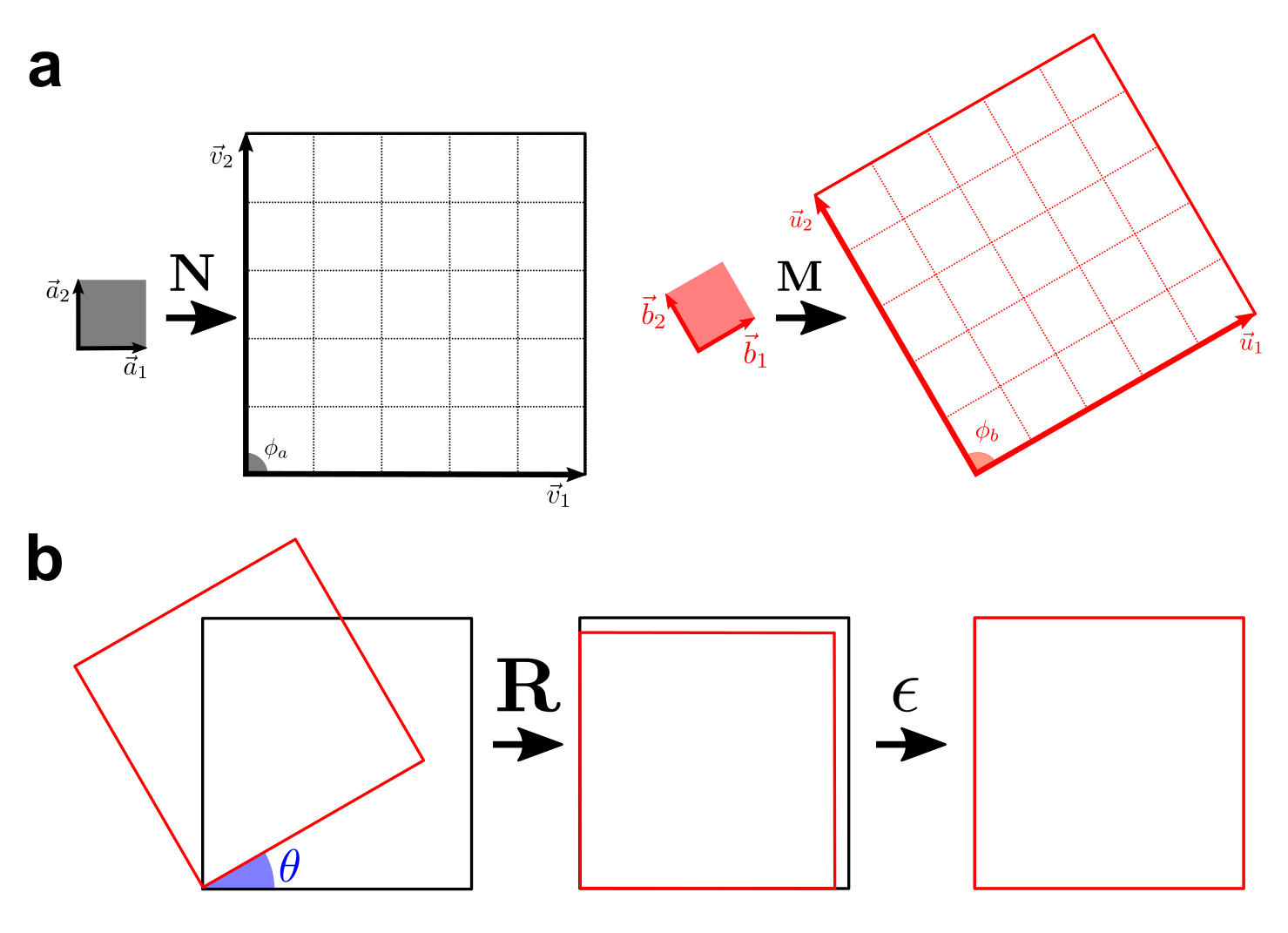
A scheme of our algorithm for surface matching is shown in Fig. 1. In order to obtain a low-strain interface structure, we systematically search through all possible 2D unit cells of the two surfaces forming the interface. Given two arbitrary surfaces and with primitive vectors and , we generate the Bravais lattices of the possible surface supercells and :
| (1) | ||||
| (2) |
In Eq. 1-2, , are repetition matrices where the entries are integers below two threshold values , , and (), () are the Bravais lattice vectors of the resulting supercells. During the generation of the supercells, we exclude equivalent lattices.
For each pair of supercells, we next determine a rotation matrix which rotates and aligns with :
| (3) |
where , with and , respectively. Finally, we match the two supercells by defining a strain tensor , which is applied to in order to match its Bravais lattice onto that of . The resulting equation to match and reads:
| (4) |
with the individual components of the strain tensor being:
| (5) | ||||
| (6) | ||||
| (7) |
A similar procedure can also be be applied to strain and match it to , or to strain equally both surfaces.
Straining one or both sides of the interface introduces and additional elastic contribution to the interface energetics. This contribution and its influence on the surface geometry varies considerably depending on the strength of the interaction between the overlayer and the substrate. For a substrate and a strained overlayer with cubic symmetry, we can write down the total energy per unit of area as(Carel et al., 1996):
| (8) |
where is the interface energy between the substrate and the overlayer, is the energy of the free surface of the overlayer, have been defined in Eq. 5-7, , , are the elastic constants of the overlayer material and is its thickness. The equation can be further simplified as
| (9) |
where
| (10) |
Neglecting interactions between the interface and the overlayer free surface and strain effects, will be independent of the interface geometry. For metals and weakly interacting interfaces, we also expect the interface energy to be rather similar for different geometries, so that the contribution of the elastic energy will be dominant and will determine the stability trend of the different geometries. On the other hand, for interfaces between semiconductors there may be a varying number of bonds at the interface, depending on the precise overlay structure. Since binding energies for covalent bonds are typically in the range 1-2 eV, the overlayer may need to have a thickness above 2 nm before the elastic energy will dominate.
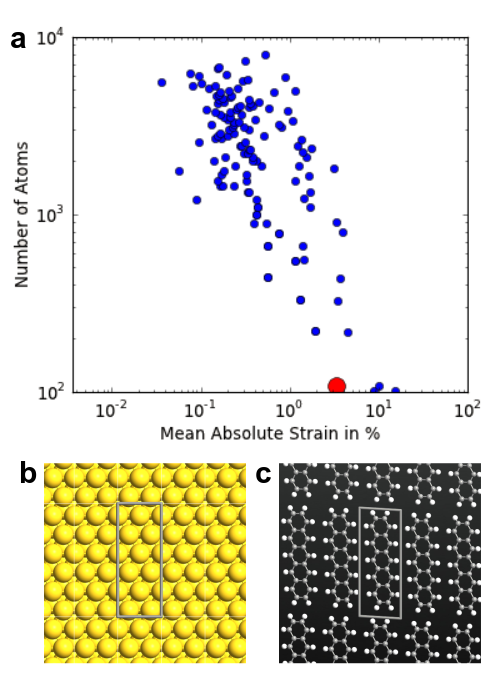
We have implemented the algorithm into the Virtual NanoLabVNL and the calculated matches are presented graphically as illustrated in Fig. 3, The plot shows the number of atoms in the supercell as function of the average strain . For the average strain we for simplicity use, . The measure in Eq. (10) gives slightly different orderings, but we found that orderings are basically similar and therefore selected the most simple option. The algorithm has been implemented to only test relevant vectors and with default values of a scan typically takes 1s and the simulation time scale as . In the next section we will apply the method to determine the structure of a Pentacene monolayer on Au(111) and the interface geometry of Al on top of InAs.
III Results
III.1 PC/Au(111)
Computational details:
The DFT calculations for PC/Au(111) have been performed using the Atomistix ToolKit (ATK, ). The Kohn-Sham orbitals have been expanded in a linear combination of pseudo-atomic orbitals (PAOs) (Junquera et al., 2001). The electronic exchange-correlation (xc) energy has been described by using the generalized gradient approximation (GGA) and the Perdew-Burke 91 (PW91) xc-functional (Wang and Perdew, 1991). We use this functional to compare with previous calculationsLi et al. (2009), however, note that the GGA-PW91 xc-functional does not include van-der-Waals forces and it will therefore underestimate adsorption energies. We have used a slab geometry with periodic boundary conditions parallel to the surface and mixed (Dirichlet+Neumann) boundary conditions in the direction normal to the surface, the latter allows for describing slabs with different workfunctions on the upper and lower surface. The Brillouin zone has been sampled using an Monkhorst-Pack (Monkhorst and Pack, 1976) grid and a Fermi-Dirac occupation scheme with a broadening of . Structural relaxations have been performed using a convergence threshold for the forces of . During both the structural optimization and the evaluation of binding energies, the basis set superimposition error (BSSE) has been corrected using the counterpoise (CP) correction scheme(Boys and Bernardi, 1970). For the Au(111) surface, only the two uppermost layers were allowed to relax during the structural optimizations, while the atoms in the lowermost layers were kept frozen at their bulk position.
For carbon we have used 21 orbitals per atom with s, p and d character and ranges up to 3.9 , while for hydrogen we have used 5 orbitals per atom with s and p character and ranges up to 4.2 . This basis set has been optimized to reproduce hydrogen and carbon dimer total energies (Blum et al., 2009). Using this basis set, we obtain an adiabatic ionization energy for the individual pentacene molecule (P1) , in good agreement with the experimentally reported value (Gruhn et al., 2002). For gold, we have used an s, p, d basis set of ranges , with a total of 9 orbitals per atom. The calculated lattice constant for bulk Au using this basis is . Using a layer of gold ghost orbitals to get a better description of the isolated Au(111) surface (García-Gil et al., 2009), we also obtain that the surface work function is . Both values are in good agreement with those obtained using similar computational parameters and a plane wave basis set (Li et al., 2009).
Results:
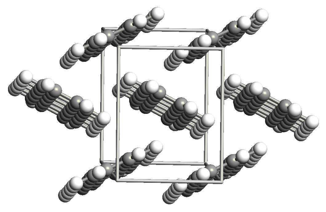
To construct the interface between the PC (see Fig.2) and Au(111), we have considered the PC unit cell according to the crystallographic parameters of Ref. 39 (P-1: , , , , , ). The internal stress calculated in this unit cell is lower than .
We have then aligned the direction of the PC unit cell along the normal to the Au(111) surface, and generated all possible interface supercells with by straining the PC lattice in the plane perpendicular to the direction. In this case, we have used the experimental lattice parameter of the Au(111) surface. Fig. 3(a) shows a graph with the resulting possible supercells, sorted according to the mean absolute strain and the number of atoms in the supercell. The lattices with lowest strain are listed in Table 1. It can be seen that supercell I, which has been used in earlier reports to model the PC/Au(111) surface (Li et al., 2009), possesses a rather large internal strain. On the other hand, our method reveals the existence of other non-trivial supercell arrangements which are associated with a much less strained PC lattice. In particular, among all the interfaces formed by a single PC(010) surface unit cell, the value of is and lower for supercell II and III, respectively.
| Structure | Au(111) | PC | ||||
|---|---|---|---|---|---|---|
| I | (2,1;0,6) | 1 | -16.0 | 10.9 | 3.3 | 10.1 |
| II | (2,0;3,6) | 1 | -3.0 | -4.0 | 2.9 | 3.3 |
| III | (2,0;-3,6) | 1 | -6.4 | -0.54 | 0.0 | 2.3 |
| IV | (2,0;-2,13) | 2 | 0.2 | 0.7 | 3.7 | 1.5 |
| V | (6,1;5,3) | 4 | -0.8 | -0.3 | -0.5 | 0.5 |
| VI | (16,-1;9,-2) | 12 | 0.0 | 0.1 | 0.1 | 0.1 |
| I-(2,1;0,6) | Li et. al.Li et al. (2009) | II-(2,0;3,6) | III-(2,0;-3,6) | Exp. | |
| (Å) | 5.11 | 5.11 | 5.90 | 5.90 | 5.64Schroeder et al. (2002) 5.76France et al. (2003) 5.7Käfer et al. (2007); Kang and Zhu (2003) |
| (Å) | 17.71 | 17.71 | 15.44 | 15.33 | 14.8Schroeder et al. (2002) 15.0France et al. (2003) 15.5Käfer et al. (2007); Kang and Zhu (2003) |
| (Å) | 3.35 | 3.1-3.5 | 3.18 | 3.17 | |
| 40 | 38 | 36 | 34 | 43Ihm et al. (2006) 31Käfer et al. (2007) | |
| 87 | 81 | 81 | 80 | ||
| (eV) | 4.25 | 4.29 | 4.48 | 4.50 | 4.52 Schroeder et al. (2002) 4.4Watkins et al. (2002) 4.6Diao et al. (2007) |
| (eV) | -0.29 | -0.16 | -0.42 | -0.42 | -1.14France et al. (2003) |
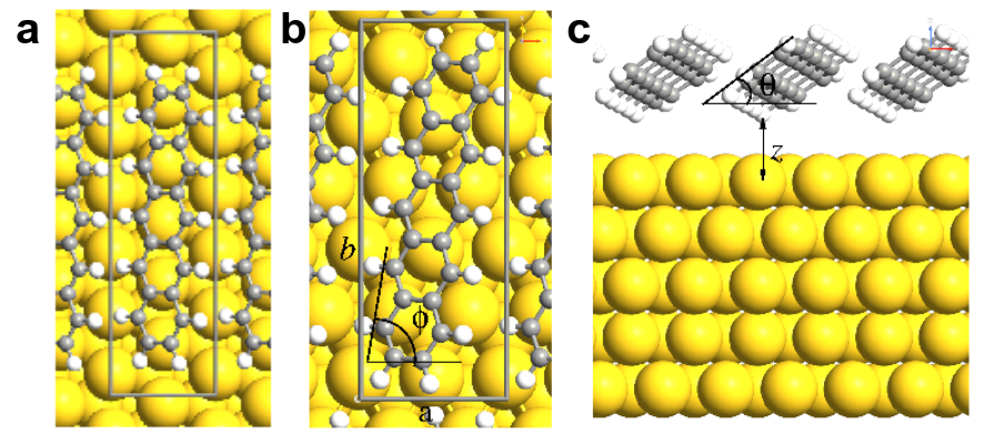
To analyze the relationship between strain and adsorption properties in PC/Au(111), we have compared the optimized geometries of supercells I, II, and III (see Table 2). For each optimized geometry we calculate the lattice vectors of the PC/Au(111) supercell, and the geometrical parameters of the PC crystal: the adsorption height and the polar and azimuthal adsorption angles and , see Fig. 4(b,c). Since supercell II and III have very similar properties, in the following we will only compare supercell I and II, see Fig. 4 (a,b). The structural parameters obtained for supercell I are very similar to those obtained using a plane wave basis set (Li et al., 2009). However, supercell II and III provides an overall better agreement with the available experimental data. In particular, the supercell lattice vectors , and the azimuthal angle are closer to those measured experimentally.
In addition to the geometrical properties, we find that the calculated work function for supercell II is also in closer agreement with that measured experimentally, compared to that calculated for supercell I. Finally, the binding energy calculated for supercell II is also larger compared to that calculated for supercell I. This indicates that the supercell II and III, in addition to providing structural parameters in better agreement with those measured experimentally, lead to a structure which is thermodynamically more favorable. We note that the discrepancy relative to the experimental value, is due to the neglect of van der Waals forces.
III.2 Al/InAs
| Structure | InAs surface | InAs | InAs | Al surface | Al | ||||
|---|---|---|---|---|---|---|---|---|---|
| I | (2,0;0,1) | 2 | (3,0;0,1) | -0.26 | -0.27 | 0 | 0.18 | ||
| II | (2,0;-1,2) | 4 | (3,0;0,3) | -0.26 | -1.79 | 0 | 0.68 | ||
| III | (0,-1;-3,0) | 3 | (-1,1;2,1) | -0.27 | -2.06 | 0 | 0.78 | ||
| IV | (2,2;0,2) | 4 | (3,3;0,3) | -0.26 | -0.26 | 0 | 0.18 | ||
| V | (2,1;1,2) | 3 | (3,2;1,3) | -2.06 | -2.06 | 0 | 1.37 | ||
| VI | (2,0;1,2) | 4 | (3,0;0,1) | -0.26 | 5.79 | 0 | 2.02 |
Following recent experimental work on InAs NWs in which superconducting properties have been induced by the proximity effect with Al (Deng et al., 2016; Albrecht et al., 2016; Higginbotham et al., 2015; Chang et al., 2015), we have considered two surfaces of InAs: the surface of the wurtzite phase (hereafter, ), and the surface of the zinc-blend phase (hereafter, ). NWs with both these surfaces orientations have been grown experimentally, and it has been demonstrated that the precise orientation of the epitaxial Al overlayer depends on the exposed InAs surface (Krogstrup et al., 2015).
For each of the two InAs surfaces, we have performed a scan over all Al surfaces with . Subsequently, for each set of Miller indexes, we have generated all possible supercells with and with a maximum of four InAs surface cells, by straining the Al lattice in the plane perpendicular to the interface.
For both the InAs surfaces considered, we have found that the Al surface which is predicted to have the lowest strain in the Al overlayer matches with that identified experimentally for thick () Al overlayers, see Table 3. In the case of InAs, this corresponds to Al, whereas in the case of InAs, this corresponds to Al.
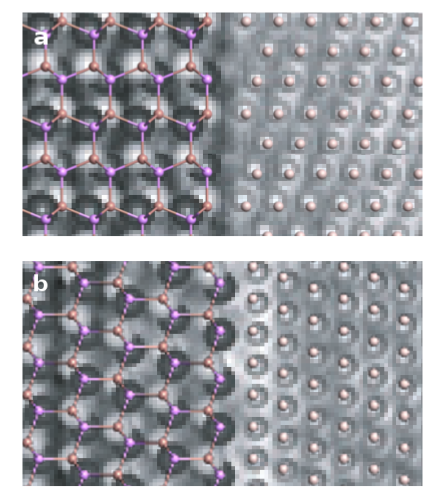
Another check on the accuracy of the method can be done by comparing the structures of the predicted InAs/Al interfaces with those measured experimentally. Fig. 5 shows the predicted InAs/Al interfaces, superimposed to the measured HR-TEM images for each interface. It can be seen that, for both interfaces, the agreement between the structural model and the HR-TEM pattern is excellent. On the InAs side of the interfaces, regions of dark and bright contrast can be associated with In and As atoms, respectively, whereas on the Al side of the interfaces, the regions with bright contrast surrounded by a darker halo can be associated with Al atoms.
IV Conclusions
In conclusion, we have presented a systematic and efficient method for determining a supercell geometry of the interface between two crystals. The method has been implemented into the Virtual NanoLab software. The method was applied to two metal-semiconductor systems, Au-Pentacene and InAs-Al interfaces. In both cases the method suggests interface geometries in good agreement with experimental data. For Au-Pentacene we illustrated that previous studiesLi et al. (2009), which does not use a systematic approach for finding a supercell geometry of the interface have lower binding energies and are not in accordance with experimental data.
Acknowledgements.
The authors acknowledges support from Innovation Fund Denmark under project 5189-00082B “Atomic-scale modelling of interfaces” and the Quantum Innovation Center (QUBIZ), Innovation Fund Denmark, and from the European Commissions Seventh Framework Programme (FP7/20072013), Grant Agreement IIIV-MOS Project No. 619326. The authors would also like to thank Erik Johnson and Peter Krogstrup for providing the NW TEM images.References
- Blom and Stokbro (2013) A. Blom and K. Stokbro, Journal of Computational Electronics 12, 623 (2013).
- Dusastre et al. (2012) V. Dusastre, J. Heber, F. Pulizzi, A. Stoddart, P. Pamies, and C. Martin, Nature Materials 11, 91 (2012).
- Kroemer (2001) H. Kroemer, Rev. Mod. Phys. 73, 783 (2001).
- Martin (2004) R. M. Martin, Electronic Structure (Cambridge University Press, Cambridge, UK, 2004).
- Stradi et al. (2016) D. Stradi, U. Martinez, A. Blom, M. Brandbyge, and K. Stokbro, Phys. Rev. B 93, 155302 (2016).
- Lazić (2015) P. Lazić, Computer Physics Communications 197, 324 (2015).
- (7) Virtual NanoLab, version 2016.2, QuantumWise A/S (2016). The Virtual NanoLab is freely available for academic researchers. www.quantumwise.com.
- Pieczyrak et al. (2011) B. Pieczyrak, E. Abad, F. Flores, and J. Ortega, J. Chem. Phys. 135, 084702 (2011).
- Li et al. (2009) H. Li, Y. Duan, V. Coropceanu, and J.-L. Bredas, Organic Electronics 10, 1571 (2009).
- Lee et al. (2007) K. Lee, J. Yu, and Y. Morikawa, Phys. Rev. B 75, 045402 (2007).
- Lee and Yu (2005) K. Lee and J. Yu, Surf. Sci. 589, 8 (2005).
- Toyoda et al. (2010) K. Toyoda, I. Hamada, K. Lee, S. Yanagisawa, and Y. Morikawa, J. Chem. Phys. 132, 134703 (2010).
- Saranyaa et al. (2012) G. Saranyaa, S. N. V. Natarajanb, P. Kolandaivela, and K. Senthilkumara, J. Mol. Graph. and Mod. 38, 334 (2012).
- Koch et al. (2007) N. Koch, A. Kahn, J. Ghijsen, J. Pireaus, J. Schwartz, R. L. Johnson, and A. Elschner, Appl. Phys. Lett. 82, 70 (2007).
- McDonald et al. (2006) O. McDonald, A. A. Cafolla, D. Carty, G. Sheerin, and G. Hughes, Surf. Sci. 600, 3217 (2006).
- Schroeder et al. (2002) P. Schroeder, C. B. France, J. B. Park, and B. A. Parkinson, J. Appl. Phys. 91, 3010 (2002).
- Ihm et al. (2006) K. Ihm, B. Kim, T.-H. Kang, K. Kim, M. H. Joo, T. H. Kim, S. S. Yoon, and S. Chung, Appl. Phys. Lett 89, 033504 (2006).
- France et al. (2003) C. B. France, P. Schroeder, J. B. Forsythe, and B. A. Parkinson, Langmuir 19, 1274 (2003).
- Käfer et al. (2007) D. Käfer, L. Ruppel, and G. Witte, Phys. Rev. B 75, 085309 (2007).
- Watkins et al. (2002) N. J. Watkins, L. Yan, and Y. Gao, Appl. Phys. Lett. 80, 4384 (2002).
- Kang and Zhu (2003) J. H. Kang and X.-Y. Zhu, Appl. Phys. Lett 82, 3248 (2003).
- Soe et al. (2009) W.-H. Soe, C. Manzano, A. D. Sarkar, N. Chandrasekhar, and C. Joachim, Phys. Rev. Lett. 102, 176102 (2009).
- Diao et al. (2007) L. Diao, C. D. Frisbie, D. D. Schroepfer, and P. P. Ruden, J. Appl. Phys. 101, 014510 (2007).
- Liu et al. (2010) Z. Liu, M. Kobayashi, B. C. Paul, Z. Bao, and Y. Nishi, Phys. Rev. B 82, 035311 (2010).
- Deng et al. (2016) M. T. Deng, S. Vaitiekėnas, E. B. Hansen, J. Danon, M. Leijnse, K. Flensberg, J. Nygård, P. Krogstrup, and C. M. Marcus, Science 354, 1557 (2016).
- Albrecht et al. (2016) S. M. Albrecht, A. P. Higginbotham, M. Madsen, F. Kuemmeth, T. S. Jespersen, J. Nygård, P. Krogstrup, and C. M. Marcus, Nature 531, 206 (2016).
- Higginbotham et al. (2015) A. P. Higginbotham, S. M. Albrecht, G. Kirŝanskas, W. Chang, F. Kuemmeth, P. Krogstrup, T. S. Jespersen, J. Nygård, K. Flensberg, and C. M. Marcus, Nat. Phys. 11, 1017 (2015).
- Chang et al. (2015) W. Chang, S. M. Albrecht, T. S. Jespersen, F. Kuemmeth, P. Krogstrup, J. Nygård, and C. M. Marcus, Nat. Nanotech. 10, 232 (2015).
- Krogstrup et al. (2015) P. Krogstrup, N. L. B. Ziino, W. Chang, S. M. Albrecht, M. H. Madsen, E. Johnson, J. Nygård, C. M. Marcus, and T. S. Jespersen, Nat. Mater. 14, 400 (2015).
- Carel et al. (1996) R. Carel, C. Thompson, and H. Frost, Acta materialia 44, 2479 (1996).
- (31) Atomistix ToolKit, version 2016.2, QuantumWise A/S (2016). www.quantumwise.com.
- Junquera et al. (2001) J. Junquera, O. Paz, D. Sánchez-Portal, and E. Artacho, Phys. Rev. B 64, 235111 (2001).
- Wang and Perdew (1991) Y. Wang and J. Perdew, Phys. Rev. B 43, 8911 (1991).
- Monkhorst and Pack (1976) H. J. Monkhorst and J. D. Pack, Phys. Rev. B 13, 5188 (1976).
- Boys and Bernardi (1970) S. F. Boys and F. Bernardi, Mol. Phys. 19, 553 (1970).
- Blum et al. (2009) V. Blum, R. Gehrke, F. Hanke, P. Havu, X. Ren, K. Reuter, and M. Scheffler, Computer Phys. Comm. 180, 2175 (2009).
- Gruhn et al. (2002) N. E. Gruhn, D. A. da Silva Filho, T. G. Bill, M. Malagoli, V. Coropceanu, A. Kahn, and J.-L. Bredas, J. Am Chem. Soc. 124, 7918 (2002).
- García-Gil et al. (2009) S. García-Gil, A. García, N. Lorente, and P. Ordejón, Phys. Rev. B 79, 075441 (2009).
- Schiefer et al. (2007) S. Schiefer, M. Huth, A. Dobrinevski, and B. Nickel, J. A. Chem. Soc. 129, 10316 (2007).
- (40) Fig. 2 of Li et. al.Li et al. (2009) shows the total energy as function of distance and the total energy is lowest at Å while the authors report Å. To address this discrepancy, the authors put the following comment: “We note that the extreme flatness of the potential energy surface in the range Å does not allow for a very accurate determination of the optimal distance.”.