A scanning gate microscope for cold atomic gases
Abstract
We present a scanning probe microscopy technique for spatially resolving transport in cold atomic gases, in close analogy with scanning gate microscopy in semiconductor physics. The conductance of a quantum point contact connected to two atomic reservoirs is measured in the presence of a tightly focused laser beam acting as a local perturbation that can be precisely positioned in space. By scanning its position and recording the subsequent variations of conductance, we retrieve a high-resolution map of transport through a quantum point contact. We demonstrate a spatial resolution comparable to the extent of the transverse wave function of the atoms inside the channel, and a position sensitivity below . Our measurements agree well with an analytical model and ab-initio numerical simulations, allowing us to identify a regime in transport where tunneling dominates over thermal effects. Our technique opens new perspectives for the high-resolution observation and manipulation of cold atomic gases.
pacs:
Scanning probe microscopes had substantial impact on the development of solid-state physics during the last three decades, from the observation of individual atoms at surfaces RevModPhys.59.615 ; RevModPhys.75.949 , to the imaging of coherent electron flow Topinka:2001aa and the identification of order parameters in complex correlated materials Fischer:2007aa ; Allan2015 – just to name a few examples. Many of these applications rely on two conceptually important ingredients: (i) the use of very sharp probes positioned with atomic-scale precision close to a surface, (ii) the ability to continuously measure transport in the presence of a local probe, which yields precise information related to a single point of the system by accumulating the often weak transport signal.
Many fundamental phenomena observed in condensed matter physics are also studied in cold-atoms based quantum simulations. This has motivated the development of high spatial resolution imaging based on photon Gemelke:2009aa ; Bakr:2009aa ; Sherson:2010aa ; PhysRevLett.114.213002 ; PhysRevLett.114.193001 ; Haller:2015aa ; PhysRevA.92.063406 ; PhysRevLett.115.263001 ; Yamamoto:2015aa ; PhysRevLett.116.175301 and electron Gericke:2008aa scattering, which typically yields a destructive observation of the local density distribution or the parity of the atom number on lattice sites. Yet, a high spatial resolution measurement in a transport setting, as has been so successfully applied in solid-state physics, has so far not been carried out with atomic gases.
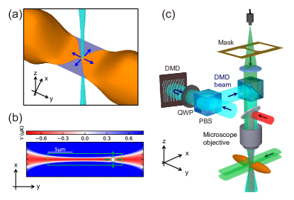
In this letter, we demonstrate a scanning gate microscope for a cold atomic gas flowing through an optically created quantum point contact (QPC) Krinner:2015aa . Our technique is inspired by scanning gate microscopy in semiconductor physics Eriksson:1996aa ; Topinka:2000aa ; Topinka:2001aa ; Sellier:2011aa , where a movable gate potential is used to locally modify the underlying carrier density in a sample. In our cold-atom implementation, we use a high-resolution optical microscope to create a sub-micrometer repulsive gate potential in the region of the QPC. Thanks to the intrinsic diluteness of cold atomic gases, our gate operates at the scale of the Fermi wavelength.
Our technique complements the direct fluorescence or absorption imaging in many respects. At the conceptual level, it uses quantum degenerate atoms themselves, rather than photons, as test particles incident on the system Imry:1999aa . Large reservoirs connected to a smaller, mesoscopic system act as source and sink for the scattered atoms, continuously accumulating the signal. Since no spontaneous emission of photons or other dissipative processes are induced during the accumulation, it is possible to access long time scales. In contrast, photon or electron scattering provide an instantaneous snapshot of the density distribution.
The basis of our experiment is a quantum degenerate Fermi gas of 6Li atoms, as described in our previous work Krinner:2015aa . The Fermi gas is produced in a combined magnetic and optical trap, yielding an elongated cloud with atoms in each of the lowest and third lowest hyperfine states of lithium. A homogeneous magnetic field of is applied, which sets the scattering length to , where is Bohr’s radius. This corresponds to an interaction parameter in the reservoirs of , where is the Fermi wavevector in the gas, is the mass of lithium atoms and is the Fermi energy in the harmonic trap, with the geometric mean of its frequencies. At typical temperatures of about we expect our gas to be in the normal phase, as the critical temperature for superfluidity is supplement . As presented in figure 1a, a repulsive potential generated by a laser beam with a nodal line in the middle is imposed on the cloud, creating a quasi two-dimensional Fermi gas at the center of the cloud, smoothly connected on both sides to large, three-dimensional reservoirs Brantut:2012aa . The trap frequency (mode spacing) along the vertical () direction at the center of the quasi two-dimensional region reaches . The QPC is produced by imaging a binary mask using light at nm, imprinting a thin wire onto the quasi two-dimensional region similar to Krinner:2015aa . We reach trap frequencies along the transverse direction of about at the center of the QPC. Along the transport direction (), the beam producing the QPC has a waist of . An attractive potential produced by a Gaussian, red-detuned beam with a waist of is superimposed onto the QPC, allowing for the control of the chemical potential in the QPC and its immediate vicinity. Upon increasing the chemical potential, successive transverse modes of the QPC are populated yielding characteristic conductance plateaus Krinner:2015aa .
The scanning gate potential is produced using light at tightly focused onto a spot with waists of and . This beam is shaped and controlled using a digital mirror device (DMD), operating in the Fourier plane of the microscope as a diffraction grating in Littrow configuration (see figure 1 and supplement ). The discreteness of the DMD sets the minimal displacement to with our optical setup.
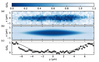
We operate the QPC in the single mode regime by tuning the chemical potential to the center of the first plateau. This condition, together with the small size of the tip and the symmetry of our potential represents a unique case, where the response of the system to the scanning gate can be interpreted as a map of the current distribution in the weak probe limit PhysRevB.88.035406 . We scan the position of the gate in the region indicated in figure 1b with an extent of . The resulting map is shown in figure 2, where each pixel represents the conductance of the QPC with the scanned gate at the position of the pixel. The individual measurements are separated by and taken with a strength of the scanning gate of . The strength is about twice the local Fermi energy at the center of the structure, corresponding to the strong probe regime Szewc2013 . The region of low conductance represents the center of the QPC, where the current density is the highest. The pattern fades out towards the edges along , where the current density is smaller due to the weaker confinements. Classically, these are regions where the extension of the gate is smaller than the width of the conductor. The full width at half maximum (FWHM) of the conductance pattern along the direction is , matching that of the beam creating the QPC. Along the transverse () direction, the short FWHM of results from the tight confinement of the QPC.
We compare the experimental results with direct numerical simulations of the scanning gate setup using the Kwant library supplement ; Groth:2014 . This solves the scattering problem of independent particles originating from ideal reservoirs and impinging onto the structure. The potential landscape of the QPC along and is set a priori from the geometry of the laser beams, and the chemical potential is adjusted to fit the data. The results of the simulation are shown in figure 2b, showing overall good agreement with the experiment. In particular, the transverse and longitudinal shapes are reproduced, as well as the fading out of the pattern in the wings of the QPC.
It was observed in the condensed matter context that scanning gate maps are dressed by fringe patterns, resulting from interferences between particles emitted by the point contact and reflected by the scanning gate Topinka:2001aa . In our experiment, these fringes are washed out by finite temperature, as confirmed by our numerical simulations supplement . In contrast to semiconductor nanostructures, where large scale disorder channels the particles emitted by the QPC Topinka:2001aa , our system is free of disorder, and channeling does not take place.
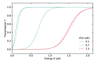
We now study the regimes of scanning gate microscopy, from weak to strong probes. To this end, we scan the gate transversally through the center of the QPC, with varying . These cuts are shown in figure 3. For the lowest , the channel is not closed even with the scanning gate at the center of the QPC. This corresponds to the weak probe regime. As is increased, the conductance quickly goes to zero when the tip is at the center, and the profile changes from approximately Gaussian to flat-top. For stronger scanning gates, the QPC is fully closed over an increasingly wide range, reflecting a clipping effect.
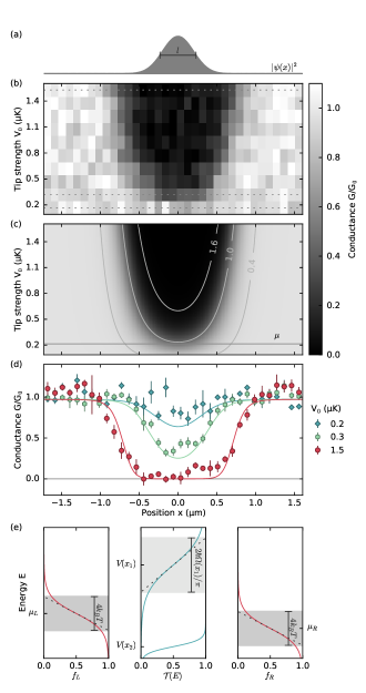
To analytically model the process we assume that the particles only explore a longitudinal cut through the Gaussian tip potential as the transverse wave function is narrower than the tip. The ground state wave function has a FWHM of inside the QPC, about half that of the tip in transverse direction. Furthermore, we approximate the potential cut in transport direction () by a parabolic barrier with anti-trapping frequency and potential offset , where is the transverse tip position with respect to the QPC center. The transmission through the parabolic barrier is given by
| (1) |
where is the energy of the incident particle Glazman:1988aa ; Ihn:2010aa . We combine the transmission with the thermal occupation of states in the reservoirs to obtain conductances, using Landauer’s formula Ihn:2010aa . The profiles calculated using this model are shown in figure 3c, where the overall chemical potential is the only free parameter common to all curves. The agreement with the measurement is good over the whole range of parameters, as can be seen on the cuts in figure 3d. We also compared this model with the numerically exact Kwant simulation, finding good agreement supplement .
Interestingly, the analytical model allows to distinguish transport based on quantum tunneling through the gate from thermally activated particles in the reservoirs. The Landauer formula includes both contributions and expresses conductance as the convolution of with the difference of the Fermi distributions. The model yields a transmission that has the same form as the Fermi distribution, allowing us to quantitatively evaluate the relative roles of tunneling and finite temperature, as illustrated in figure 3e. We can access regimes where tunneling dominates over thermal effects meaning Affleck1981 , as presented in figure 3c. This is in strong contrast with experiments in condensed matter physics where direct tunneling through the scanned gate is negligible.
The non-linearity of the transmission coefficient in equation (1) has important consequences for the spatial resolution. To estimate the resolution we measure the FWHM of the transverse cuts of figure 3 supplement . The results are presented in figure 4a, as a function of . For strong gates the FWHM is large because the QPC is already blocked by the raising edges of the Gaussian gate. Reducing , the FWHM goes down and becomes smaller than that of the laser beam for . Interestingly, it keeps decreasing for lower , showing that the resolution is not limited by the optical beam profile, analogous to super-resolved optical techniques reaching resolutions beyond the diffraction limit Novotny:2012aa . For the smallest , the signal is weak but the FWHM is low enough to be comparable with that of the transverse ground state wave function in the QPC. It agrees with the analytical model, which also predicts very strong thermal broadening for weak scanning gates.
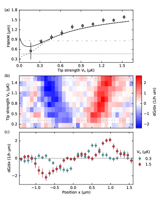
While weak gates allow for high spatial resolution, strong gates maximize the position sensitivity, because small position changes can yield large variations in conductance. This is the case in the raising edges of a strong scanning gate, and is widely exploited in scanning gate microscopy in the solid state context Sellier:2011aa . To study this effect, we extract the derivative of conductance with position , as shown in figure 4b supplement . The extremal variation rates mark the falling edges of the profiles and separate with increasing gate strength. The evolution of the width of the profile is clearly visible, as well as the clipping regime when the strong scanning gate is located at the center of the QPC. The fastest variations amount to per micrometer.
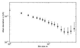
The position sensitivity of our apparatus is limited by the signal to noise ratio with which we can measure conductances. The figure of merit is , where is the noise in the conductance measurement. To assess the minimal noise we use the overlapping Allan deviation Riley:2008aa , giving 111We performed 128 repeated conductance measurements in the single mode regime without scanning gate. The Allan deviation becomes minimal upon binning 29 consecutive measurements. supplement . This translates into a position sensitivity of . The sensitivity characterizes our instrument, and is mainly limited by the shot-to-shot noise in the preparation of the reservoirs.
Since the scanned gate is optically generated with programmable holograms, the same setup could be used to project several gates, with tailored shapes, serving as building blocks for more complex atomtronics circuits Albiez:2005aa ; Pepino:2009aa ; PhysRevA.82.013640 ; Eckel:2014aa ; Husmann:2015ab ; Valtolina:2015ab ; PhysRevA.93.063619 . Time-modulated or near-resonant optical gates that address external or internal atomic degrees of freedom could allow to locally generate effective gauge structures. Such gates could also be used to perform spectroscopic measurements in analogy with scanning tunneling microscopy PhysRevLett.115.165301 .
Our scanning gate technique can be generalized to any cold atoms system in which conductance measurements can be performed, such as disordered systems Shapiro:2012aa , yielding the additional ability to control the potential at a scale shorter than the localization length. It could distinguish percolation processes from localization by interferences, or be combined with density measurements to identify the fraction of the atoms participating in transport Krinner:2015ac . In superfluid Fermi gases the scanning gate could manipulate local modes like Andreev bound states Husmann:2015ab ; Valtolina:2015ab . It could also help to identify dynamical structures such as vortex patterns Beria:2013aa .
Acknowledgements.
We acknowledge discussions with A. Georges, T. Giamarchi, and thank B. Bräm, L. Corman, R. Desbuquois, R. Steinacher, P. Törmä, D. Weinmann and W. Zwerger for discussions and careful reading of the manuscript. We acknowledge financing from NCCR QSIT, the ERC project SQMS, the FP7 project SIQS, the Horizon2020 project QUIC, Swiss NSF under division II. SN acknowledges support from JSPS. JPB is supported by the Ambizione program of the Swiss NSF and by the Sandoz Family Foundation-Monique de Meuron program for Academic Promotion I.References
- (1) G. Binnig and H. Rohrer, Rev. Mod. Phys. 59, 615 (1987).
- (2) F. J. Giessibl, Rev. Mod. Phys. 75, 949 (2003).
- (3) M. A. Topinka, B. J. LeRoy, R. M. Westervelt, S. E. J. Shaw, R. Fleischmann, E. J. Heller, K. D. Maranowski, and A. C. Gossard, Nature 410, 183 (2001).
- (4) O. Fischer, M. Kugler, I. Maggio-Aprile, C. Berthod, and C. Renner, Rev. Mod. Phys. 79, 353 (2007).
- (5) M. P. Allan, K. Lee, A. W. Rost, M. H. Fischer, F. Massee, K. Kihou, C.-H. Lee, A. Iyo, H. Eisaki, T.-M. Chuang, et al., Nat. Phys. 11, 177 (2015).
- (6) N. Gemelke, X. Zhang, C. Hung, and C. Chin, Nature 460, 995 (2009).
- (7) W. S. Bakr, J. I. Gillen, A. Peng, S. Fölling, and M. Greiner, Nature 462, 74 (2009).
- (8) J. F. Sherson, C. Weitenberg, M. Endres, M. Cheneau, I. Bloch, and S. Kuhr, Nature 467, 68 (2010).
- (9) M. F. Parsons, F. Huber, A. Mazurenko, C. S. Chiu, W. Setiawan, K. Wooley-Brown, S. Blatt, and M. Greiner, Phys. Rev. Lett. 114, 213002 (2015).
- (10) L. W. Cheuk, M. A. Nichols, M. Okan, T. Gersdorf, V. V. Ramasesh, W. S. Bakr, T. Lompe, and M. W. Zwierlein, Phys. Rev. Lett. 114, 193001 (2015).
- (11) E. Haller, J. Hudson, A. Kelly, D. A. Cotta, B. Peaudecerf, G. D. Bruce, and S. Kuhr, Nat. Phys. 11, 738 (2015).
- (12) G. J. A. Edge, R. Anderson, D. Jervis, D. C. McKay, R. Day, S. Trotzky, and J. H. Thywissen, Phys. Rev. A 92, 063406 (2015).
- (13) A. Omran, M. Boll, T. A. Hilker, K. Kleinlein, G. Salomon, I. Bloch, and C. Gross, Phys. Rev. Lett. 115, 263001 (2015).
- (14) R. Yamamoto, J. Kobayashi, T. Kuno, K. Kato, and Y. Takahashi, New J. Phys. 18, 023016 (2016).
- (15) E. Cocchi, L. A. Miller, J. H. Drewes, M. Koschorreck, D. Pertot, F. Brennecke, and M. Köhl, Phys. Rev. Lett. 116, 175301 (2016).
- (16) T. Gericke, P. Wurtz, D. Reitz, T. Langen, and H. Ott, Nat. Phys. 4, 949 (2008).
- (17) S. Krinner, D. Stadler, D. Husmann, J.-P. Brantut, and T. Esslinger, Nature 517, 64 (2015).
- (18) M. A. Eriksson, R. G. Beck, M. Topinka, J. A. Katine, R. M. Westervelt, K. L. Campman, and A. C. Gossard, Appl. Phys. Lett. 69, 671 (1996).
- (19) M. A. Topinka, B. J. LeRoy, S. E. J. Shaw, E. J. Heller, R. M. Westervelt, K. D. Maranowski, and A. C. Gossard, Science 289, 2323 (2000).
- (20) H. Sellier, B. Hackens, M. G. Pala, F. Martins, S. Baltazar, X. Wallart, L. Desplanque, V. Bayot, and S. Huant, Semicond. Sci. Technol. 26, 064008 (2011).
- (21) Y. Imry and R. Landauer, Rev. Mod. Phys. 71, S306 (1999).
- (22) See Supplemental Material at [URL will be inserted by publisher] for details.
- (23) J.-P. Brantut, J. Meineke, D. Stadler, S. Krinner, and T. Esslinger, Science 337, 1069 (2012).
- (24) S. Krinner, M. Lebrat, D. Husmann, C. Grenier, J.-P. Brantut, and T. Esslinger, PNAS 113, 8144 (2016).
- (25) C. Gorini, R. A. Jalabert, W. Szewc, S. Tomsovic, and D. Weinmann, Phys. Rev. B 88, 035406 (2013).
- (26) W. Szewc, Theory and Simulation of Scanning Gate Microscopy, Theses, Université de Strasbourg (2013).
- (27) C. W. Groth, M. Wimmer, A. R. Akhmerov, and X. Waintal, New J. Phys. 16, 063065 (2014).
- (28) L. I. Glazman, G. B. Lesovik, D. E. Khmel’Nitskiǐ, and R. I. Shekhter, ZhETF Pisma Redaktsiiu 48, 218 (1988).
- (29) T. Ihn, Semiconductor Nanostructures (Oxford University Press, 2010).
- (30) I. Affleck, Phys. Rev. Lett. 46, 388 (1981).
- (31) L. Novotny and B. Hecht, Principles of nano-optics (Cambridge University Press, 2012).
- (32) W. Riley, Handbook of frequency stability analysis (2008).
- (33) M. Albiez, R. Gati, J. Fölling, S. Hunsmann, M. Cristiani, and M. K. Oberthaler, Phys. Rev. Lett. 95, 010402 (2005).
- (34) R. A. Pepino, J. Cooper, D. Z. Anderson, and M. J. Holland, Phys. Rev. Lett. 103, 140405 (2009).
- (35) R. A. Pepino, J. Cooper, D. Meiser, D. Z. Anderson, and M. J. Holland, Phys. Rev. A 82, 013640 (2010).
- (36) S. Eckel, J. G. Lee, F. Jendrzejewski, N. Murray, C. W. Clark, C. J. Lobb, W. D. Phillips, M. Edwards, and G. K. Campbell, Nature 506, 200 (2014).
- (37) D. Husmann, S. Uchino, S. Krinner, M. Lebrat, T. Giamarchi, T. Esslinger, and J.-P. Brantut, Science 350, 1498 (2015).
- (38) G. Valtolina, A. Burchianti, A. Amico, E. Neri, K. Xhani, J. A. Seman, A. Trombettoni, A. Smerzi, M. Zaccanti, M. Inguscio, et al., Science 350, 1505 (2015).
- (39) S. Eckel, J. G. Lee, F. Jendrzejewski, C. J. Lobb, G. K. Campbell, and W. T. Hill, Phys. Rev. A 93, 063619 (2016).
- (40) A. Kantian, U. Schollwöck, and T. Giamarchi, Phys. Rev. Lett. 115, 165301 (2015).
- (41) B. Shapiro, J. Phys. A 45, 143001 (2012).
- (42) S. Krinner, D. Stadler, J. Meineke, J.-P. Brantut, and T. Esslinger, Phys. Rev. Lett. 115, 045302 (2015).
- (43) M. Beria, Y. Iqbal, M. Di Ventra, and M. Müller, Phys. Rev. A 88, 043611 (2013).
I Supplemental material
I.1 Experimental details
I.1.1 Experimental cycle
To produce degenerate Fermi gases, we first create a mixture of the two lowest hyperfine states of 6Li and balance the populations using several incomplete Landau-Zener sweeps. Forced evaporation at a magnetic field of cools the atoms to about the Fermi temperature. Subsequently, a complete Landau-Zener transition transfers the full population from the second to the third lowest hyperfine state, and the magnetic field is ramped to a Feshbach resonance at . A magnetic field gradient induces the final evaporation and the magnetic field is ramped in to , setting the scattering length for transport to . The gas resides in a hybrid trap, where an optical dipole trap confines transversally (, ), while the atoms are longitudinally () restricted by a magnetic field curvature. The trapping frequencies along and are and and in direction .
A chemical potential bias is induced by shifting the cloud in transport direction using a magnetic field gradient of about . We then split the cloud asymmetrically with an elliptical repulsive beam into two reservoirs. By moving the magnetic trap back to its symmetric position, the atom number difference translates into a chemical potential bias. In the presence of the QPC the transport process is started by removing the repulsive beam and terminated by switching it back on again after a transport time of . Finally, we infer the density distribution using absorption imaging along the direction.
I.1.2 Calibration of the quantum point contact
The QPC provides harmonic confinement along the transverse directions (, ) that we calibrate as follows. We measure the transverse trapping frequency by parametrically modulating the intensity of the laser beam restricting the atoms in direction. Close to the resonance the atoms are heated and escape from a dipole trap created by a laser beam that propagates along the axis and tightly confines the atoms to the center.
Then, we calibrate the frequency by measuring transport in the quantized regime, where the conductance plateaus energetically shift with the transverse confinement. Hence, a change in confinement along the axis can be compensated with the one along , linking the unknown frequency to the calibrated one. Practically, we relate the two frequencies indirectly via calibrating each of them against a red-detuned beam that controls the chemical potential in the vicinity of the QPC. As a byproduct this beam is calibrated, which is relevant to characterize the scanning gate.
I.1.3 Calibration of the scanning gate
The strength of the scanning gate is extracted using transport. To this end, we center the gate on the channel and balance the added repulsion with a red-detuned beam (see red beam in figure 1c), previously calibrated. As the gate is tightly focused it easily blocks transport even at the highest achievable local chemical potentials. Hence, we enlarge the gate to waists of and to distribute the power and reduce the peak intensity.
Simultaneously, we image the scanning gate with a high-resolution microscope on a CCD sensor. Thanks to the measured local chemical potential shift the registered number of counts per exposure time is converted to the potential created on the atoms. With this the potential strength of the narrow scanning gate can be read from an image.
I.1.4 Holographic beam shaping
We operate a digital mirror device (DMD DLP5500 .55” XGA from Texas Instruments) to create and move the scanning gate beam, while compensating for optical aberrations. It consists of a grid of micrometer sized square mirrors, which can be individually flipped about their diagonal axis to two stable positions (ON and OFF) at an angle of .
When all mirrors have the same orientation coherent light is diffracted into several orders. We send a collimated beam at onto the DMD incident at an angle close to , where the Littrow and the blazing condition are both fulfilled for the order. In this configuration the diffraction and incident angles are identical and almost aligned with the specular reflection. This leads to a compact optical setup and a near-optimal diffraction efficiency of . The pattern imprinted on the DMD is later imaged on the back focal plane of a microscope objective, which effectively projects its Fourier transform onto the atomic plane.
To correct aberrations and shape the beam, we control its phase locally by an amplitude hologram. We display a grating where groups of several consecutive mirrors in ON respectively OFF state are alternating. By shifting the grating locally we modify the phase of the light Zupancic2016 . The displayed grating has a larger spacing and hence additional diffraction orders appear. We use one directly neighboring the main order, whose orientation relative to the hologram plane is controlled by the spacing and direction of the pixel grating. The orientation of this order then directly translates to its position in the atomic plane.
An identical microscope objective is placed symmetrically after the atomic plane to image the light potential. Cropping small apertures onto the DMD and fitting the position of their images through the optical system allows to retrieve the local tilt of the wavefront, similar to a Hartmann-Shack analysis. The tilt information is integrated to obtain a transverse spatial map of the beam phase, which is then compensated by distorting the lines of the initial grating to eliminate beam aberrations. We estimate a residual wavefront distortion of around .
I.2 Data analysis
I.2.1 Temperature extraction
For the temperature measurement, we ramp the magnetic field to a Feshbach resonance at and image the cloud. With the virial theorem valid at unitarity Thomas2005 we determine the energy per particle from the second moment of the density distribution and translate it to entropy per particle by means of the known equation of state Ku2012 ; Guajardo2013 . To trace back the temperature to the BCS regime, we assume that the magnetic field is swept adiabatically Krinner2016 . Hence, the entropy at unitarity equals the one in the BCS regime, which reads for a weakly interacting, degenerate Fermi gas Carr2004 ; Su2003
| (S1) |
with the Fermi temperature , the mean trapping frequency and the corresponding wavevector . With an interaction strength of the lowest order correction yields a value that is by larger than the non-interacting case, supporting the expansion in . We obtain typical temperatures around .
At these temperatures we expect our gas to be in the normal phase, as shown in the following. The critical temperature for superfluidity is locally largest at the center of the trap, where additionally an attractive beam increases the density. As a result the local Fermi temperature is about at our parameters, giving a local interaction strength of . Thus, BCS theory including Gorkov and Melik-Barkhudarov corrections Pethick2002 , predicts a critical temperature of . This is an upper bound as we neglect the presence of the repulsive beams forming the wire.
I.2.2 Chemical potential bias extraction
We infer the chemical potential bias initially prepared between the two reservoirs from the trapping geometry, the number of atoms, the temperature and the interaction. In each reservoir the potential is harmonic along the and direction and half-harmonic in the direction. Assuming a weakly interacting and degenerate Fermi gas in the left reservoir, the chemical potential reads Su2003
| (S2) |
with the Fermi temperature , where the factor of two considers the half-harmonic confinement, and the corresponding wavevector . Analogously, the formula holds for the right reservoir and the bias is given by and is typically . The correction terms for finite temperature and interaction reduce the chemical potential each by about compared to the non-interacting case.
I.2.3 Conductance evaluation
We infer the conductance from the exponentially decaying atom number difference between the left and right reservoir as described in Krinner2015 . Apart from the measured decay constant we need the compressibility of a single reservoir. It is calculated as based on the equation of state (S2) for a weakly interacting, degenerate Fermi gas and is given by
| (S3) |
where the quantities are evaluated at the same number of atoms . The Fermi temperature reads and the corresponding Fermi wavevector is denoted by . The temperature correction term decreases the compressibility by , while the term for interactions increases it by compared to the non-interacting value.
I.2.4 Full width at half maximum of the transverse scans
From the transverse cuts in figure 3 we extract the full width at half maximum (FWHM) by fitting the profiles for each tip strength separately. As the profiles vary from bell-shaped to flat-top, we use a modified Gaussian function inspired by the eigenstates of a harmonic oscillator, that we expect to faithfully describe the profiles. It reads
| (S4) |
with the transverse position of the tip and of the channel’s center. The parameter measures the width of the Gaussian function that is modified by the Hermite polynomials and their coefficients . As the profiles are symmetric about the channel, we only include the even polynomials up to order . The order is chosen as small as possible while still reproducing the curves well and ranges practically from zero to six. The offset indicates the conductance when the gate position tends to infinity.
We evaluate the FWHM and its uncertainty numerically from the fitted function. The FWHM is given by the width at half maximum of , while the uncertainty is obtained by shifting the half maximum level by the averaged standard error over the profile.
I.2.5 Numerical derivative of the transverse scans
The spatial derivative shown in figure 4 is evaluated separately for each transverse profile (see figure 3) at fixed tip strength. We extract the local slope using a weighted linear fit over four consecutive points, while its abscissa is the mean abscissa over the window. The weight includes the averaged standard error over the profile and leads to the uncertainty in the slope. We then shift the window by one point and repeat the method.
I.2.6 Conductance noise estimation
Generally, the measured conductances contain noise of different types and timescales as well as drifts that we need to separate. For example, white noise may be reduced upon averaging, while drifts worsen the result the more we average. To determine the minimal uncertainty, we perform an Allan analysis. This technique was initially developed to assess the stability of atomic clocks Allan1966 and is more widely used nowadays, for example to characterize optical tweezers Czerwinski2009 .
The basis of an Allan analysis is a time series of observations , , …, equally spaced by the measurement interval . The Allan variance is calculated as Howe1981 ; Riley2008
| (S5) |
where are the observations averaged over consecutive points 222Formula (10) in Riley2008 correctly gives the overlapping Allan variance, while formula (9) is wrong. The full inner sum should be squared and not just its summands.. The bins are overlapping to obtain the best estimate of the Allan variance and it is equal to the classical version if the data are random and uncorrelated. Similarly, the Allan variance follows a chi-squared distribution that allows to estimate the confidence in the result. The degrees of freedom of the distribution is reduced due to the correlations among the bins and empirically given by (Howe1981, , equation (6.6)).
To assess the noise present in the conductance, we performed 128 repeated measurements in the single mode regime in the absence of the scanning gate. Figure S1 presents the Allan deviation of the conductance as a function of the bin size . With increasing bin size the deviation first decreases down to upon averaging 29 consecutive measurements, and then increases due to drifts in our apparatus. Although the minimal reachable noise of has asymmetric uncertainties, we conservatively assume the larger of the two limits, giving .
I.3 Numerical simulations
We use the Kwant package Groth2014 to compute the total transmission through the QPC in presence of a repulsive gate potential. The quasi two-dimensional region separating the large atom reservoirs is discretized on a two-dimensional mesh covering an area in the - plane. The potential is simplified as the sum of the wire and scanning gate potential, since the attractive gate and optical dipole trap can be considered as uniform at the scale of the QPC.
The total transmission through the scattering region is then obtained by summing over all single-particle transport modes of the reservoirs along the transverse -direction. We compute the conductance using a modified Landauer formula
| (S6) |
that now includes the contributions of every single mode in the transverse -direction through an energy shift , assuming harmonic confinement along . Each contribution to the total conductance is broadened by
| (S7) |
the difference between the Fermi-Dirac distributions at chemical potentials and and temperature . Chemical potential is here defined as , the reservoir Fermi energy augmented by the attractive top-gate potential, and reduced by the zero-point energy along .
In the end, we obtain scanning gate maps of the conductance by numerically performing the integral (S6) for scattering potentials with different positions of the gate. The chemical potential imbalance and temperature used are extracted from time-of-flight pictures of the reservoirs, whereas the absolute chemical potential is obtained from a best fit to the experimental data.
I.3.1 Fringe patterns in scanning gate maps
In solid state samples scanning gate maps reveal fringe patterns, resulting from interferences between particles emitted by the point contact and reflected back by the scanning gate Topinka2001 . However, they are absent in our measured and simulated maps in figure 2. In this section we pinpoint the reason by studying the influence of averaging due to finite temperature and finite chemical potential bias.
As a reference, we study the case of zero temperature and infinitesimal bias, where the conductance reduces to for the first transverse mode in -direction. Figure S2 presents scanning gate maps in this limit for three different chemical potentials, close to the transverse zero-point energy of the QPC. They are dressed by interferences, fading out as the gate is moving away. The fringes stem from multiple reflections between the gate and the QPC, reminescent of Topinka2001 . Some features of the pattern are understood with the aid of the effective potential in figure S2d, which includes the transverse confinement in -direction. As the particle moves outwards it gains kinetic energy and hence the phase of its wave function evolves faster, leading to a denser appearance of the resonances. Furthermore, they broaden as the transmission through the gate monotonically increases with higher kinetic energy.
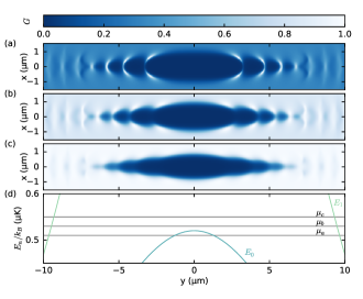
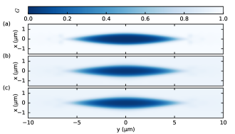
The conductance at finite temperature, as well as at finite chemical potential bias is an average of the transmission for different particle energies. As the fringes move with the incident particle energy, they are blurred upon averaging. Taken separately, both finite bias and temperature are enough to wash out the interferences, shown in figure S3a and b. The combined effect can be seen in panel c.
I.3.2 Transverse scans
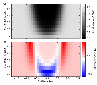
In figure 3 we study the transport of atoms through the channel as a function of the transverse position of the tip and its strength and interpret the experiment with an analytical model rooted in the Landauer formalism. Here, we investigate the numerical predictions based on the Kwant package and compare it to the results of the analytical model.
Figure S4 presents the predicted conductance as a function of the transverse tip position and its strength. Both models include the chemical potential as the only free parameter which is fitted against measured data, while the temperature and chemical potential bias are independently calibrated to and . The optimized chemical potentials are for the analytical and for the numerical model. The reference of the chemical potential differs by the transverse mode energy of along the axis, in quantitative agreement with the fitted values. Additionally, the predicted conductances deviate at most by justifying the analytical model.
I.4 Analytical model
To analytically model the transverse scans presented in figure 3 we employ the Landauer formalism Ihn2010 . It describes the conductance through a one-dimensional channel connected to two reservoirs that are independently in thermal equilibrium, given for a single occupied transverse mode by
| (S8) |
Each reservoir is characterised by a Fermi-Dirac distribution or respectively centred around the chemical potentials and , biased by and with a temperature . The channel is incorporated in the energy-dependent transmission that is dominated by the narrowest part of the constriction Glazman1988 .
At the narrowest place we neglect the extent of the transverse wave function compared to the potential created by the scanning gate tip. Hence the particles only explore a cut of the Gaussian tip potential along the transport direction ()
| (S9) |
where and are the corresponding waists. To obtain an analytical expression for the transmission we approximate the Gaussian potential by a parabolic barrier
| (S10) |
with a potential offset and anti-trapping frequency depending on the transverse tip position .
| (S11) | |||
| (S12) |
The transmission through the parabolic barrier reads Kemble1935
| (S13) |
and we use it to approximate the transmission through the Gaussian barrier, valid for particles with energies above zero.
Finally, we calculate the conductance as a function of the transverse tip position and strength by numerically integrating the expression (S8) with the transmission through a parabolic barrier given in formula (S13). The chemical potential bias and the temperature are independently calibrated from absorption images, while the overall chemical potential is a free parameter fitted to the experimental data in figure 3b.
I.4.1 Validity of the parabolic approximation
Figure S5 compares the transmission through a Gaussian and a parabolic barrier for various potential offsets and hence also anti-trapping frequencies. In the experiment the offset ranges from essentially zero, when the tip is weak and far apart from the QPC, up to for the strongest tip placed at the center. With increasing offset the transition from zero to unit transmission is shifted to higher particle energies. At the same time the anti-trapping frequency increases as the potential barrier gets sharper and the transition gets broader due to quantum tunnelling and reflections. The transmission through the parabolic barrier faithfully approximates the one through the Gaussian obstacle and only slightly underestimates it around the barrier top . The deviations increase for lower barrier heights.
References
- (1) P. Zupancic, P. M. Preiss, R. Ma, A. Lukin, M. E. Tai, M. Rispoli, R. Islam, and M. Greiner, Opt. Express 24, 13881 (2016).
- (2) J. E. Thomas, J. Kinast, and A. Turlapov, Phys. Rev. Lett. 95, 120402 (2005).
- (3) M. J. H. Ku, A. T. Sommer, L. W. Cheuk, and M. W. Zwierlein, Science 335, 563 (2012).
- (4) E. R. S. Guajardo, M. K. Tey, L. A. Sidorenkov, and R. Grimm, Phys. Rev. A 87, 063601 (2013).
- (5) S. Krinner, M. Lebrat, D. Husmann, C. Grenier, J.-P. Brantut, and T. Esslinger, PNAS 113, 8144 (2016).
- (6) L. D. Carr, G. V. Shlyapnikov, and Y. Castin, Phys. Rev. Lett. 92, 150404 (2004).
- (7) G. Su, J. Chen, and L. Chen, Phys. Lett. A 315, 109 (2003).
- (8) C. J. Pethick and H. Smith, Bose-Einstein condensation in dilute gases (Cambridge University Press, 2002).
- (9) S. Krinner, D. Stadler, D. Husmann, J.-P. Brantut, and T. Esslinger, Nature 517, 64 (2015).
- (10) D. W. Allan, Proceedings of the IEEE 54, 221 (1966).
- (11) F. Czerwinski, A. C. Richardson, and L. B. Oddershede, Opt. Express 17, 13255 (2009).
- (12) D. A. Howe, D. U. Allan, and J. A. Barnes, in Thirty Fifth Annual Frequency Control Symposium. 1981 (1981), pp. 669–716.
- (13) W. Riley and D. A. Howe, Handbook of Frequency Stability Analysis, NIST Special Publication 1065, NIST (2008).
- (14) C. W. Groth, M. Wimmer, A. R. Akhmerov, and X. Waintal, New J. Phys. 16, 063065 (2014).
- (15) M. A. Topinka, B. J. LeRoy, R. M. Westervelt, S. E. J. Shaw, R. Fleischmann, E. J. Heller, K. D. Maranowski, and A. C. Gossard, Nature 410, 183 (2001).
- (16) T. Ihn, Semiconductor Nanostructures (Oxford University Press, 2010).
- (17) L. I. Glazman, G. B. Lesovik, D. E. Khmel’Nitskiǐ, and R. I. Shekhter, ZhETF Pisma Redaktsiiu 48, 218 (1988).
- (18) E. C. Kemble, Phys. Rev. 48, 549 (1935).
- (19) E. Hairer, S. P. Nørsett, and G. Wanner, Solving ordinary differential equations I (Springer, 1993).