Layer dependent electronic structure changes in transition metal dichalcogenides- The microscopic origin
Abstract
We have examined the electronic structure evolution in transition metal dichalcogenides MX2, where M=Mo,W and X=S,Se and Te. These are generally referred to as van der Waals heterostructures on the one hand, yet one has band gap changes as large as 0.6 eV with thickness in some instances. This does not seem to be consistent with a description where the dominant interactions are van der Waals interactions. Mapping onto a tight binding model allows us to quantify the electronic structure changes which are found to be dictated solely by interlayer hopping interactions. Different environments that an atom encounters could change the Madelung potential and therefore the onsite energies. This could happen while going from monolayer to bilayer as well as in cases where the stackings are different from what is found in 2H structures. These effects are quantitatively found to be negligible, enabling us to quantify the thickness dependent electronic structure changes as arising from interlayer interactions alone.
1 Introduction
Although the transition metal dichalcogenides have been studied for fifty plus years, it is amazing that novel phenomena are still being discovered in these materials. Additionally the current thrust for alternate technologies have led to their successful use in catalysis, in addition to explorations in photovoltaics, nanoelectronics etc 1, 2, 3, 4, 5. Analogous to the nanomaterials where one finds a size dependence of the band gap 6, 7, 8, one finds thickness dependent changes in the electronic structure of the layered transition metal dichalcogenides9, 10, 11, 12 . Additionally one finds a thickness dependent band gap which changes character. The bulk band gap (optical) of MoS2 is found to be an indirect one of 1.3 eV 9 which increases to 1.6 eV in the bilayer limit 10. The nature of the band gap changes and becomes a direct one of 1.9 eV at the monolayer limit 11. The fact that the monolayers of Mo and W-based transition metal dichalcogenides have a direct band gap (with the exception of WSe2 13) is evident from the sharp peak that one finds in the photoluminescence spectra14 . MoSe2 also has an indirect band gap of 1.1 eV 9 in the bulk limit whereas in the monolayer limit it has direct band gap of about 1.66 eV 12. A smaller change is found in the bandgap of MoTe2 in contrast to MoS2 and MoSe2. Here one finds the indirect bulk band gap of 0.9 eV changes to 1.1 eV at the monolayer limit. Considering the W-based analogues, one has a change of 0.75 eV in WS2, while one has a smaller change of 0.45 eV in WSe2 15, 16, 17.
There could be different types of MX2 (M = Mo, W, Ti etc., X = S, Se, etc.) sandwiches depending on the coordination of the transition metal atom with the chalcogens as well as the stacking of atoms 18, 19. In this work we focus our attention on the 2H polymorph of MX2 (M=Mo,W, X=S,Se,Te)20, 21, 22, 23 where the symmetry about the Mo/W site is trigonal prismatic, though certain generic features are found to be valid across different types of stacking 19. The bonding within each monolayer is strongly covalent. However, the coupling between layers is believed to be due to weak van der Waals interaction. This has led to the multilayers being called van der Waals heterostructures. Hence the changes in the band gap, which was found to be as large as 0.75 eV in WS2 15 seems surprising.
A popular method to examine the size dependent electronic structure of semiconductor nanostructures has been the tight- binding model. The size dependence within the model emerges from two effects. The first is the changed coordination of the atom which could affect the Madelung potential and therefore the onsite energies of the levels on that atom. The second is the change in the bandwidth due to reduced coordination faced by some of the atoms. Usually only the latter effects are considered. In the context of the transition metal dichalcogenides, however, the effects due to the former become important as unlike in the nanostructures where a small fraction of the atoms have different coordination, here, a significant fraction have a coordination different from the bulk. A mapping onto a tight binding model allows us to explore for the first time the role of various contributions leading to quantum confinement.
The issue of the origin of the size dependence of the bandgap in TMDs has been addressed earlier in the literature 24. Zhang and Zunger 25 examined the electronic structure as a function of thickness and identified the variations seen to arise from two factors - the kinetic energy controlled quantum confinement as well as the potential energy controlled level repulsion. Kang and coworkers 26 suggest that the crystal symmetries of hexagonal layered materials lead to a weak interlayer coupling of the band extrema at the K point. Modifications in the local symmetry for instance break these symmetries and allow for the emergence of an electronic structure that depends on thickness. Cappelluti et al. 27 have fit the band structure for a monolayer of MoS2 to a nearest neighbour tight-binding model. The same parameters were used for the bilayer with additionally interlayer interactions thrown in. This was then used to infer that it is the interlayer interactions that were responsible for the electronic structure changes in MoS2 with thickness, especially the direct to the indirect bandgap transition. Among other attempts of tight binding based studies, there have been a large number of studies determining the relevant tight-binding parameters 28, 29, 30, 31. These studies have started with different basis set choices. The values of the parameters entering the tight-binding Hamiltonian have been determined either by fitting the band structure in a small energy window in the vicinity of the band gap or constraining the model to reproduce some physical parameters such as the band gap, hole/electron effective mass, the location of the valence band maximum and the conduction band minimum. In some instances, a non-orthogonal basis set has been used28, 31. This has the disadvantage that the extracted onsite energies do not correspond to the natural orbital energy and one cannot discuss trends across the series where the anion is changed for instance. Further, one usually prefers to work with a model using an orthogonal basis while including many body effects.
We build on the ideas given in the literature. As mentioned earlier, the changed environment could lead to modifications in the Madelung potentials associated with the atoms and consequently changes in the onsite energy. This was not considered earlier. Further a mapping of the band structure over a wider range of energy allows us to describe the trends in the electronic structure better. For this reason we carry out a mapping of the electronic structure as a function of thickness for Mo- and W- based TMDs. We have fixed the interlayer distances at the values at which all the calculations are reported in ths manuscript, and then calculated the electronic structure after switching off the van der Waals interactions. A similar mapping of the band structure onto a tight-binding model was carried out. We find that there is no change in the onsite energies of the bilayers of TMDs from the values that we had including van der Waals interactions. This implies that the van der Waals interactions determine the interlayer seperation. However, they do not modify the electronic structure. Additionally in each of the systems studied, we find that switching off the interlayer hopping interactions for the bilayers and beyond, we are able to recover the monolayer bandstructure. This demonstrates that even in materials in which the interaction between layers is believed to be van der Waals type, it is covalent interactions between the layers that determines the evolution of the electronic structure with an increase in the number of layers. Consequently a knowledge of the tight-binding Hamiltonian for the monolayer as well as the strength of the interlayer hopping interactions allows us to construct the Hamiltonian for any number of layers. While the discussion so far has focussed on the stacking that is favoured in the bulk structures, the 2H stacking, alternate stackings are also possible. Considering bilayers of MoSe2, steric effects between the electrons on the two layers determine the interlayer separations for different stackings. However, one finds that the nature of stacking has very small effect on the onsite energies which are again found to be the same as the monolayer by a similar analysis. These results imply that even while modeling twisted bilayers of these materials, the variations we find in the electronic structure emerge from the interlayer interactions which has been the approach adopted in the literature. Our analysis in the present work show that the inclusion of weak van der Waals interactions in the Hamiltonian governing the electronic structure does not change the onsite energies and is only responsible for determining the interlayer separation. Building on these arguments, our conclusion that the electronic structure evolution with number of layers of TMDs are mainly determined by the interlayer hopping interactions stands robust.
2 Results and Discussion
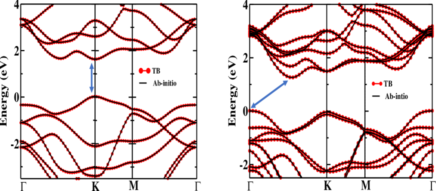
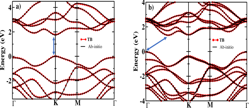
The band dispersions for monolayer MoSe2 along various symmetry directions are plotted in Fig. 1(a). One finds that the valence band maximum (VBM) and the conduction band minimum (CBM) are both located at K point and the system is a direct band gap semiconductor. This is consistent with experiment which also finds the system to be a direct band gap semiconductor with a gap of 1.66 eV. While the experimental band gap is the optical band gap12., in our calculations we are calculating the single particle gap. The present calculations which use generalized gradient approximation (GGA) for the exchange correlation functional find a gap of 1.59 eV which is close to the experimental value. The agreement is however fortuitous as one usually has an underestimation of the band gap due to self-interaction effects among various other approximations which enter the use of the generalized gradient approximation in the absence of an exact exchange correlation functional. In order to quantify the changes in the electronic structure, we have mapped the band structure onto a tight binding model with Mo and Se states in the basis. The tight binding band structure shown by red line with circles is superposed on the calculated band structure in Fig. 1(a). We have a good description of the band structure in the energy window from -3.5 eV to 4 eV. This gives us confidence in the extracted parameters and allows us to discuss changes in the electronic structure in terms of these parameters.
There are several ways to construct the bilayer of MoSe2. Each monolayer can be visualized as a three atomic layer stacking of Mo and Se atoms where Mo atoms are sandwiched between layers of Se atoms. The Se atoms generate a trigonal prismatic crystal field at the Mo site. The stacking that we have considered has the Mo atom in one layer above that in the layer beneath. However, the Mo-Se motif is rotated by 180∘ in the upper layer with respect to the layer beneath. This is referred to as the AA′ stacking and has been shown to have the lowest energy among various stacking patterns considered 18, 19.
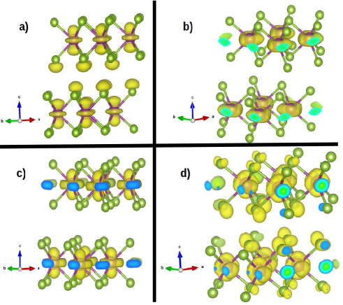
Considering a bilayer of MoSe2, we have calculated the band dispersions along various symmetry directions. This is shown in Fig. 1(b). We find that the VBM which was at K point has now shifted to . The CBM is also shifted to T point which lies along the line from to K. This leads to an indirect band gap of 1.25 eV in contrast to the experimental value of 1.55 eV 10. The changeover in the VBM positions can easily be understood by examining the character of the states contributing to this point. This is shown in Fig. 2 where we plot the charge density for the highest occupied band at in panel (a).
These are seen to emerge from the interactions between the orbitals on Mo and orbitals on Se. As these involve orbitals which are directed out of plane, one finds that these levels in the lower layer interact with the / orbitals in the layer above. As a result, the highest occupied band at point moves to higher energies relative to that at K point, and consequently the VBM shifts to point when we move from monolayer to bilayer. The highest occupied band at the K point is contributed by interactions between in-plane orbitals as is evident from Fig. 2(b). Hence it shows no shift in the bilayer from its position for the monolayer. A similar analysis of the charge density contributing to the lowest unoccupied band at T and K symmetry points is shown in panels (c) and (d) of Fig. 2. We find that in-plane orbitals contribute to the lowest unoccupied band at K point while out-of-plane orbitals contribute to the lowest unoccupied band at T point. Hence, the increased interaction arising from the presence of the second layer moves T point relative to K point, making the former the conduction band minimum. These ideas are consistent with the analysis of Padhila et al. 32 who examined the movement of various band extrema as a function of the number of layers in MoS2.
While these ideas are qualitative, we examine the extracted onsite energies and hopping interaction strengths in order to make a more quantitative statement of the role of various effects which determine the electronic structure. As mentioned earlier, we have a good description of the electronic structure within the tight binding model. This gives us confidence in the extracted parameters. The onsite energies for Se as well as Mo orbitals extracted by the tight binding mapping for monolayer as well as bilayer MoSe2 are given in Table LABEL:onsite. In order to undertand the role of weak van der Waals interaction on the electronic structure of MoSe2, we first fixed the interlayer seperation at the value used for the calculations for the bilayer in the manuscript and then switched off the van der Waals interactions. The extracted energies were found to be the same as given in Table LABEL:onsite but with a constant shift. It is hence clear from this analysis that the van der Waals term does not modify the Hamiltonian describing the electronic structure of TMDs but enters only the total energy and plays the role of getting the correct interlayer seperation in these systems.
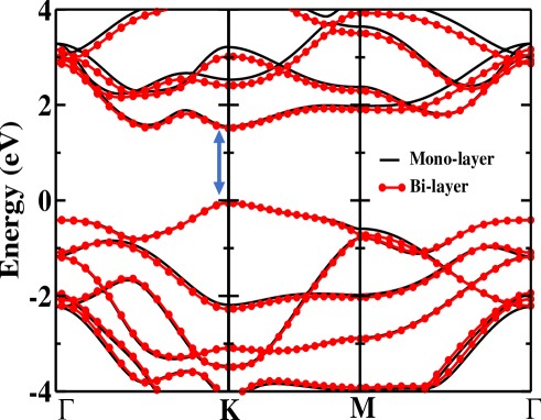
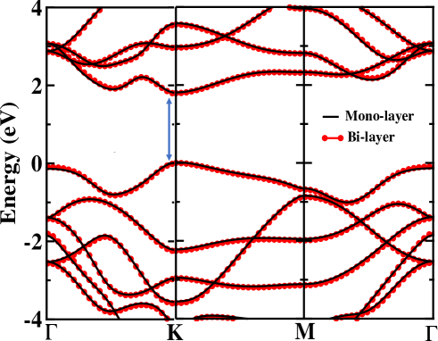
After inspection of the onsite energies, one can conclude that the Madelung potential differences for the atoms in the bilayer as compared to the monolayer are very small. This validates the approximation of using the same onsite energies for each layer in several earlier studies in the literature. In order to examine what is it that leads to the differences in the electronic structure in going from monolayer to bilayer, we have considered the tight binding Hamiltonian for the bilayer. All the interlayer interactions have been switched off in this Hamiltonian and the ensuing band structure has been plotted along various symmetry directions in Fig. 3. The band structure for the monolayer has been superposed for comparison. The two band structures look almost identical suggesting that the only difference between the electronic structure of the monolayer and that for the bilayer emerge from interlayer interactions. The dominant interaction strengths are found between the orbitals on first (3.72 Å) neighbor as well as second (5.92 Å) neighbor Se atoms.
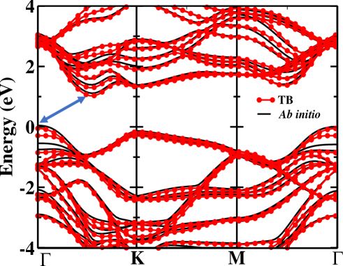
In order to examine this hypothesis further, we constructed a trilayer heterostructure of MoSe2. The band structure for the trilayer was calculated along various symmetry directions. This is shown in Fig.4. For comparison and to examine the hypothesis made vis-a-vis the origin of the changes in the electronic structure as each layer is added, we set up the tight binding Hamiltonian for the trilayer. This was done by considering the Hamiltonian for the monolayer for each of the layers. The interlayer interactions extracted for the bilayer were then used to couple the layers. The band structure calculated within this model was superposed on the band structure for the trilayer in Fig. 4. The comparison is reasonably good, justifying our hypothesis. These results clearly show that the electronic structure changes in going from the monolayer to bilayer and beyond are derived from interlayer hopping interactions alone.
This is a surprising result as the nomenclature used for these systems is van der Waals heterostructures. This would have us believe that the dominant interaction is van der Waals interactions. However our analysis suggests that covalent interactions determine the modification in the electronic structure with thickness. This is not entirely surprising as the nearest neighbor separations between Se atoms of two layers is 3.718 Å. While the nearest neighbor distance of two Se atoms in the same layer is 3.289 , assuming a Harrison-type scaling law for the distance, one finds that the hopping interaction strengths for the interlayer hopping interaction strengths drop to 70% of the values within the layer. Hence the presence of finite hopping interaction strengths for electrons in the two layers is not entirely surprising. This immediately raises the question of the role played by van der Waals interactions. This interlayer separation for the bilayer is found to be 3.99 Å when van der Waals interactions are not included and 3.19 Å when they are. Hence their inclusion merely predicts the interlayer separation.
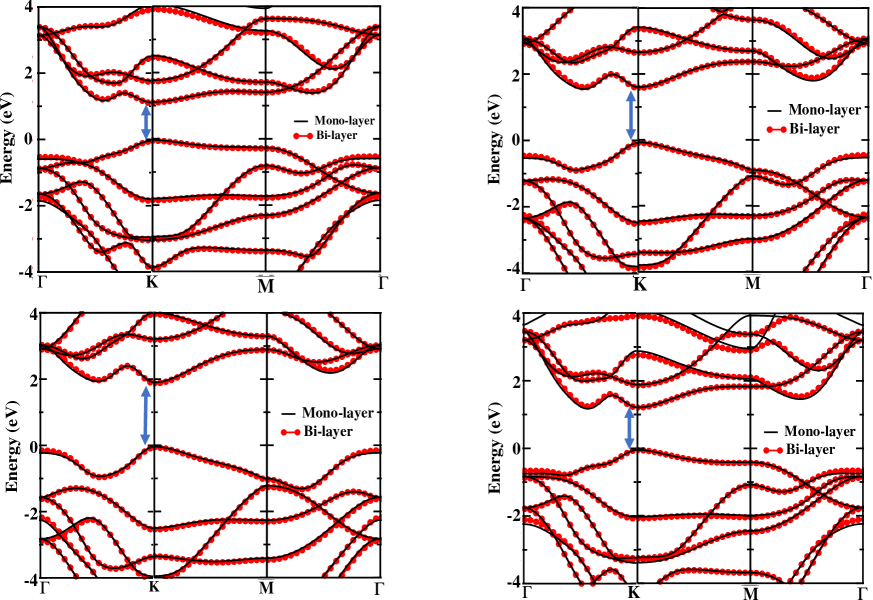
While we have examined the onsite energies in going from monolayer to bilayer for the 2H stacking, there are other stackings possible. In order to examine whether our conclusions were general enough, we considered bilayers with AA, A′B, AB′ and AB stacking which are shown in Fig. 5 19. As the environment for each atom in the monolayer as well as the bilayer are different in each case, we expect changes in the Madelung potential. In each case the band structure was fit to a tight binding model with Mo and Se states in the basis. The extracted onsite energies are given in Table LABEL:mose3_all_stack. These onsite energies for different stacking of layers in MoSe2 bilayer are similar to what we found in the case of 2H stacking (Table LABEL:onsite). Hence the changed environment for different stackings have very little effect on the onsite energies, and electronic structure changes emerge from the differing interlayer interactions. This is consistent with the approach adopted in the literature to examine the electronic structure of twisted bilayers 33. Some of the previous studies on twisted bilayer graphene and silicene reported changes in local density of states in different stacking areas34, 35.
The evolution of the electronic structure with number of layers that we find here is not specific to MoSe2 alone. We find similar changes when we examine the electronic structure as a function of the number of layers for MoS2 also. In Fig. 6 we have plotted the band structure for the monolayer in panel (a) and for the bilayer in panel (b). The tight-binding band structure has been superposed in each case and we have a good description of the band structure. A comparison of the extracted onsite energies is given in Table LABEL:onsitemos2. These extracted values of the onsite energies are in agreement with the values available in the literature 30.
Here again, we find that the energies for the monolayer and bilayer are similar, as we found earlier. When we considered the tight binding Hamiltonian for the bilayer and switched off interlayer interactions, we recovered the monolayer band structure. The comparison between the tight binding Hamiltonian results with interlayer interactions switched off and the band structure for the monolayer is given in Fig. 7. In order to demonstrate that the conclusions obtained from our analysis of MoSe2 and MoS2 are general, we have considered a monolayer as well as bilayers of MoTe2, WS2, WSe2 and WTe2. The band dispersions calculated for the monolayer of each of these systems along various symmetry directions is shown in Fig.8. The band structure for the bilayer was mapped onto a tight binding model with maximally localized Wannier functions for the radial part. The ensuing band structure for the bilayers, with interlayer interactions switched off, has been superposed on the monolayer band structure in Fig.8. The two are found to be almost identical for each of the systems shown here, indicating that the differences in the electronic structure between monolayer and bilayer arise due to interlayer interactions alone.
3 Conclusions
In conclusion, we have examined the evolution in the electronic structure of transition metal dichalcogenides as a function of layers. The changes in the structure that one finds have been discussed in terms of a combination of interlayer hopping interactions as well as Madelung potential effects. In each case, a mapping of the electronic structure onto a tight binding model with transition metal and anion states in the basis allows us to quantify the role of each of these effects. Even in these layered materials which are referred to as van der Waals heterostructures, we find that interlayer hopping interactions play the primary role in bringing about changes in the electronic structure as a function of thickness. Expected Madelung potential variations on the other hand, we find, play no role in the observed changes in electronic structure. These ideas are valid across the MX2 where M = (Mo, W) and X = (S, Se, Te). While most results discussed in the manuscript correspond to the 2H stacking, we show that considering other types of stackings does not change the conclusions.
4 Methodology
The electronic structure calculations of monolayer and bilayer MX2 (M=Mo,W X=S,Se,Te) have been carried out within a plane wave implementation of density functional theory (DFT) within VASP 36 (Vienna Simulation Package). We have taken the 2H stacking of the bilayers in each case as it is found to be the most stable structure 19. While, the lattice constants are kept at the experimental values for MX2 series (M=Mo,W X=S,Se,Te )20, 21, 22, 23 which are listed in Table LABEL:lc_encut , all the atoms are allowed to relax through a total energy minimization that is guided by the calculated atomic forces. A vacuum of 20 Å is used along direction to minimize the interaction among the periodic images for the monolayer. Projected augmented wave 37, 38 potentials are used to solve the electronic structure self-consistently using a k-points mesh of 1212 1. Cutoff energies for the plane wave basis states in material series MX2 (M=Mo,W X=S,Se,Te) are also listed in Table LABEL:lc_encut . Perdew-Burke-Ernzerhof (PBE) 39 approximation was used for the exchange-correlation functional. The weak van der Waals interaction between the layers has an effect in the determination of the interlayer distances. A dispersion correction based on Grimme’s DFT-D2 method 40 is used on top of the PBE potentials.
In order to quantify the results, we setup the following tight binding model with the transition metal and anion states in the basis.
where creates (annihilates) an electron in the th orbital on transition metal site in the th unit cell while creates (annihilates) an electron in the th orbital on oxygen atom in the th unit cell. In this model, the maximally localized Wannier functions 41 are used for the radial parts of the basis functions. Technically, the degree of localization and the symmetry of these Wannier functions can be controlled in the projection procedure. All on-site energies and hopping interaction strengths in this case are determined from the interface of VASP to Wannier90 42. Once a full tight-binding Hamiltonian is obtained for the bilayers, in order to switch off the interlayer interactions, we identify all the interlayer terms in and and put corresponding ’s to zero. Apart from the 2H stacking, for MoSe2, we also explored other stacking geometries AA, A′B, AB′ and AB shown in Fig. 519 to explore the renormalization of the onsite energies due to differing Madelung potentials.
5 Author Information
S. K. Pandey and Ruma Das contributed equally to this work. Queries should be addressed to priya.mahadevan@gmail.com.

| Material | Lattice constant (Å) | Cut-off energy (eV) |
|---|---|---|
| MoS2 | 3.150 | 350 |
| MoSe2 | 3.289 | 280 |
| MoTe2 | 3.519 | 280 |
| WS2 | 3.153 | 350 |
| WSe2 | 3.282 | 280 |
| WTe2 | 3.491 | 280 |
| Orbitals | Monolayer MoSe2 | Bilayer MoSe2 |
|---|---|---|
| Se- | 0.00 | +0.01 |
| Se- | 0.00 | 0.0 |
| Se- | -0.33 | -0.38 |
| Mo- | +1.46 | +1.51 |
| Mo- | +2.28 | +2.31 |
| Mo- | +2.28 | +2.31 |
| Mo- | +1.46 | +1.52 |
| Mo- | +1.20 | +1.27 |
| Orbitals | AA | A′B | AB′ | AB |
|---|---|---|---|---|
| Se- | 0.0 | 0.0 | 0.0 | 0.0 |
| Se- | 0.0 | 0.0 | 0.0 | 0.0 |
| Se- | -0.35 | -0.36 | -0.35 | -0.35 |
| Mo- | +1.52 | +1.53 | +1.50 | +1.51 |
| Mo- | +2.30 | +2.31 | 2.29 | +2.30 |
| Mo- | +2.30 | +2.31 | 2.29 | +2.30 |
| Mo- | +1.52 | +1.53 | +1.50 | +1.51 |
| Mo- | +1.28 | +1.28 | +1.25 | +1.26 |
| Orbitals | Monolayer MoS2 | Bilayer MoS2 | BL MoSe230 |
|---|---|---|---|
| S- | 0.00 | 0.0 | 0.0 |
| S- | 0.00 | 0.0 | 0.0 |
| S- | -0.28 | -0.25 | -0.52 |
| Mo- | +1.66 | +1.69 | +1.39 |
| Mo- | +2.68 | +2.69 | +2.36 |
| Mo- | +2.68 | +2.69 | +2.36 |
| Mo- | +1.65 | +1.68 | +1.39 |
| Mo- | +1.46 | +1.47 | +1.15 |
References
- Hu et al. 2018 Hu, C.; Yuan, C.; Hong, A.; Guo, M.; Yu, T.; Luo, X. Work function variation of monolayer MoS2 by nitrogen-doping. Applied Physics Letters 2018, 113, 041602
- Hu et al. 2019 Hu, C.; Jiang, Z.; Zhou, W.; Guo, M.; Yu, T.; Luo, X.; Yuan, C. Wafer-Scale Sulfur Vacancy-Rich Monolayer MoS2 for Massive Hydrogen Production. The Journal of Physical Chemistry Letters 2019, 10, 4763–4768, PMID: 31381350
- Feng et al. 2016 Feng, Q.; Yan, F.; Luo, W.; Wang, K. Charge trap memory based on few-layer black phosphorus. Nanoscale 2016, 8, 2686–2692
- Lv et al. 2018 Lv, Q.; Yan, F.; Wei, X.; Wang, K. High-Performance, Self-Driven Photodetector Based on Graphene Sandwiched GaSe/WS2 Heterojunction. Advanced Optical Materials 2018, 6, 1700490
- Wei et al. 2019 Wei, X.; Yan, F.; Lv, Q.; Zhu, W.; Hu, C.; Patanè, A.; Wang, K. Enhanced Photoresponse in MoTe2 Photodetectors with Asymmetric Graphene Contacts. Advanced Optical Materials 2019, 7, 1900190
- Nanda et al. 2000 Nanda, J.; Sapra, S.; Sarma, D. D.; Chandrasekharan, N.; Hodes, G. Size-selected Zinc Sulfide Nanocrystallites: Synthesis, Structure and Optical Studies. Chemistry of Materials 2000, 12, 1018–1024
- Ithurria et al. 2011 Ithurria, S.; Tessier, M. D.; Mahler, B.; Lobo, R. P. S. M.; Dubertret, B.; Efros, A. L. Colloidal nanoplatelets with two-dimensional electronic structure. Nat. Mater. 2011, 10, 936–941
- Viswanatha et al. 2004 Viswanatha, R.; Sapra, S.; Satpati, B.; Satyam, P. V.; Dev, B. N.; Sarma, D. D. Understanding the quantum size effects in ZnO nanocrystals. J. Mater. Chem. 2004, 14, 661–668
- Böker et al. 2001 Böker, T.; Severin, R.; Müller, A.; Janowitz, C.; Manzke, R.; Voß, D.; Krüger, P.; Mazur, A.; Pollmann, J. Band structure of and Angle-resolved photoelectron spectroscopy and ab initio calculations. Phys. Rev. B 2001, 64, 235305
- Tongay et al. 2012 Tongay, S.; Zhou, J.; Ataca, C.; Lo, K.; Matthews, T. S.; Li, J.; Grossman, J. C.; Wu, J. Thermally Driven Crossover from Indirect toward Direct Bandgap in 2D Semiconductors: MoSe2 versus MoS2. Nano Lett. 2012, 12, 5576–5580
- Mak et al. 2010 Mak, K. F.; Lee, C.; Hone, J.; Shan, J.; Heinz, T. F. Atomically Thin : A New Direct-Gap Semiconductor. Phys. Rev. Lett. 2010, 105, 136805
- Shaw et al. 2014 Shaw, J. C.; Zhou, H.; Chen, Y.; Weiss, N. O.; Liu, Y.; Huang, Y.; Duan, X. Chemical vapor deposition growth of monolayer MoSe2 nanosheets. Nano Research 2014, 7, 511–517
- Zhang et al. 2015 Zhang, C.; Chen, Y.; Johnson, A.; Li, M.-Y.; Li, L.-J.; Mende, P. C.; Feenstra, R. M.; Shih, C.-K. Probing Critical Point Energies of Transition Metal Dichalcogenides: Surprising Indirect Gap of Single Layer WSe2. Nano Letters 2015, 15, 6494–6500
- Splendiani et al. 2010 Splendiani, A.; Sun, L.; Zhang, Y.; Li, T.; Kim, J.; Chim, C.-Y.; Galli, G.; Wang, F. Emerging Photoluminescence in Monolayer MoS2. Nano Letters 2010, 10, 1271–1275
- Braga et al. 2012 Braga, D.; Gutiérrez Lezama, I.; Berger, H.; Morpurgo, A. F. Quantitative Determination of the Band Gap of WS2 with Ambipolar Ionic Liquid-Gated Transistors. Nano Letters 2012, 12, 5218–5223, PMID: 22989251
- Wilson and Yoffe 1969 Wilson, J.; Yoffe, A. The transition metal dichalcogenides discussion and interpretation of the observed optical, electrical and structural properties. Advances in Physics 1969, 18, 193–335
- Zhao et al. 2013 Zhao, W.; Ghorannevis, Z.; Chu, L.; Toh, M.; Kloc, C.; Tan, P.-H.; Eda, G. Evolution of Electronic Structure in Atomically Thin Sheets of WS2 and WSe2. ACS Nano 2013, 7, 791–797, PMID: 23256505
- Chhowalla et al. 2013 Chhowalla, M.; Shin, H. S.; Eda, G.; Li, L.-J.; Loh, K. P.; Zhang, H. The chemistry of two-dimensional layered transition metal dichalcogenide nanosheets. Nature Chemistry 2013, 5, 263–275
- He et al. 2014 He, J.; Hummer, K.; Franchini, C. Stacking effects on the electronic and optical properties of bilayer transition metal dichalcogenides , , , and . Phys. Rev. B 2014, 89, 075409
- Bronsema et al. 1986 Bronsema, K. D.; De Boer, J. L.; Jellinek, F. On the structure of molybdenum diselenide and disulfide. Zeitschrift für anorganische und allgemeine Chemie 1986, 540, 15–17
- Coehoorn et al. 1987 Coehoorn, R.; Haas, C.; Dijkstra, J.; Flipse, C. J. F.; de Groot, R. A.; Wold, A. Electronic structure of , , and . I. Band-structure calculations and photoelectron spectroscopy. Phys. Rev. B 1987, 35, 6195–6202
- Schutte et al. 1987 Schutte, W.; Boer, J. D.; Jellinek, F. Crystal structures of tungsten disulfide and diselenide. Journal of Solid State Chemistry 1987, 70, 207 – 209
- Dawson and Bullett 1987 Dawson, W. G.; Bullett, D. W. Electronic structure and crystallography of MoTe2and WTe2. Journal of Physics C: Solid State Physics 1987, 20, 6159–6174
- Kuc et al. 2011 Kuc, A.; Zibouche, N.; Heine, T. Influence of quantum confinement on the electronic structure of the transition metal sulfide S2. Phys. Rev. B 2011, 83, 245213
- Zhang and Zunger 2015 Zhang, L.; Zunger, A. Evolution of Electronic Structure as a Function of Layer Thickness in Group-VIB Transition Metal Dichalcogenides: Emergence of Localization Prototypes. Nano Letters 2015, 15, 949–957, PMID: 25562378
- Kang et al. 2016 Kang, J.; Zhang, L.; Wei, S.-H. A Unified Understanding of the Thickness-Dependent Bandgap Transition in Hexagonal Two-Dimensional Semiconductors. Journal of Physical Chemistry Letters 2016, 7, 597–602
- Cappelluti et al. 2013 Cappelluti, E.; Roldán, R.; Silva-Guillén, J. A.; Ordejón, P.; Guinea, F. Tight-binding model and direct-gap/indirect-gap transition in single-layer and multilayer MoS2. Phys. Rev. B 2013, 88, 075409
- Rostami et al. 2013 Rostami, H.; Moghaddam, A. G.; Asgari, R. Effective lattice Hamiltonian for monolayer MoS2: Tailoring electronic structure with perpendicular electric and magnetic fields. Phys. Rev. B 2013, 88, 085440
- Liu et al. 2013 Liu, G.-B.; Shan, W.-Y.; Yao, Y.; Yao, W.; Xiao, D. Three-band tight-binding model for monolayers of group-VIB transition metal dichalcogenides. Phys. Rev. B 2013, 88, 085433
- Fang et al. 2015 Fang, S.; Kuate Defo, R.; Shirodkar, S. N.; Lieu, S.; Tritsaris, G. A.; Kaxiras, E. Ab initio tight-binding Hamiltonian for transition metal dichalcogenides. Phys. Rev. B 2015, 92, 205108
- Zahid et al. 2013 Zahid, F.; Liu, L.; Zhu, Y.; Wang, J.; Guo, H. A generic tight-binding model for monolayer, bilayer and bulk MoS2. AIP Advances 2013, 3, 052111
- Padilha et al. 2014 Padilha, J. E.; Peelaers, H.; Janotti, A.; de Walle, C. G. V. Nature and evolution of the band-edge states in : From monolayer to bulk. Phys. Rev. B 2014, 90, 205420
- Suárez Morell et al. 2010 Suárez Morell, E.; Correa, J. D.; Vargas, P.; Pacheco, M.; Barticevic, Z. Flat bands in slightly twisted bilayer graphene: Tight-binding calculations. Phys. Rev. B 2010, 82, 121407
- 34 Zhao, M.; Zhuang, J.; Cheng, Q.; Hao, W.; Du, Y. Moiré-Potential-Induced Band Structure Engineering in Graphene and Silicene. Small n/a, 1903769
- Li et al. 2018 Li, Z.; Zhuang, J.; Wang, L.; Feng, H.; Gao, Q.; Xu, X.; Hao, W.; Wang, X.; Zhang, C.; Wu, K.; Dou, S. X.; Chen, L.; Hu, Z.; Du, Y. Realization of flat band with possible nontrivial topology in electronic Kagome lattice. Science Advances 2018, 4
- Kresse and Furthmüller 1996 Kresse, G.; Furthmüller, J. Efficient iterative schemes for ab initio total-energy calculations using a plane-wave basis set. Phys. Rev. B 1996, 54, 11169–11186
- Kresse and Joubert 1999 Kresse, G.; Joubert, D. From ultrasoft pseudopotentials to the projector augmented-wave method. Phys. Rev. B 1999, 59, 1758–1775
- Blöchl 1994 Blöchl, P. E. Projector augmented-wave method. Phys. Rev. B 1994, 50, 17953–17979
- Perdew et al. 1996 Perdew, J. P.; Burke, K.; Ernzerhof, M. Generalized Gradient Approximation Made Simple. Phys. Rev. Lett. 1996, 77, 3865–3868
- Grimme 2006 Grimme, S. Semiempirical GGA-type density functional constructed with a long-range dispersion correction. J. Comput. Chem. 2006, 27, 1787–1799
- Mostofi et al. 2008 Mostofi, A. A.; Yates, J. R.; Lee, Y.-S.; Souza, I.; Vanderbilt, D.; Marzari, N. wannier90: A tool for obtaining maximally-localised Wannier functions. Comput. Phys. Commun. 2008, 178, 685 – 699
- Franchini et al. 2012 Franchini, C.; Kováčik, R.; Marsman, M.; Murthy, S. S.; He, J.; Ederer, C.; Kresse, G. Maximally localized Wannier functions in LaMnO 3 withinPBE + U , hybrid functionals and partially self-consistent GW: an efficient route to construct ab initio tight-binding parameters for e g perovskites. J. Phys.: Condens. Matter 2012, 24, 235602