Valence band structure calculations of strained Ge1-xSnx quantum well pFETs
Abstract
The dependence of valence band structures of Ge1-xSnx with 0 0.2 on Sn content, biaxial strain, and substrate orientation is calculated using the nonlocal empirical pseudopotential method. The first valence subband structure in p-type Ge cap/fully strained Ge1-xSnx quantum well/Ge (001) and (111) inversion layers are theoretically studied using the 66 kp model. A wave-function coupling of a Ge cap with respect to a strained Ge1-xSnx quantum well, which is influenced by the cap thickness, valence band offset, and confined effective mass, changes the energy dispersion relation in the two-dimensional -space. The increase in Sn content and the decrease in cap thickness increase the hole population in the strained Ge1-xSnx quantum well to reduce the transport effective mass at the zone center in the Ge/strained Ge1-xSnx/Ge inversion layers.
-
March 6 2017
1 Introduction
Sn incorporating into Ge potentially makes Ge1-xSnx alloys as a direct-gap semiconductor [1, 2, 3, 4, 5], which make them suitable for use in n-channel field effect transistors (nFETs) owing to the small effective mass of the valley [6]. Several studies on GeSn pFETs show high hole mobilities of strained GeSn grown on Ge (001) [7, 8], (110) [9], and (111) [10, 11] substrates. The reduction in effective mass along the channel direction () due to biaxial compressive strain is responsible for the increased hole mobility [8, 12]. In GeSn/Ge (001), the biaxial compressive strain lifts the light hole band along the [110] direction [8]. Increasing the Sn content can further reduce the light hole effective mass [4]. In addition, the Ge cap on the GeSn channel can prevent holes from scatterings at the Ge/oxide interface [8]. Nevertheless, knowledge of valence subband structures in GeSn inversion layers is very limited owing to the unknown 66 kp Luttinger parameters and deformation potential parameters of GeSn alloys. Note that linearly interpolated 66 kp parameters based on the linear virtual crystal approximation (VCA) have been widely used in calculations related to valence subband structures in the SiGe inversion layers [13, 14]. Low’s pioneering approach [4] fitted multiple sets of nonlinear Luttinger parameters (, , and ) of relaxed GeSn alloys from full-band structures calculated using the nonlocal empirical pseudopotential method (EPM) for discrete Sn content. However, this approach increases the computational complexity, as it requires taking different strains and proportions of Sn content into account. In this work, one set of 66 kp parameters for Ge1-xSnx alloys, where 0 0.2 with in-plane biaxial strain of 3% 1%, are fitted based on the calculated valence band structures and effective masses of strained GeSn (001), (110), and (111) wafer orientations using EPM. The fitted 66 kp parameters are used to calculate the valence subband structures in inversion layers of Ge cap/10 nm GeSn quantum well (QW)/Ge (001) and (111) pFETs. Most of the holes in these cases are located in the first subband, of which favorable for carrier transport is implied by a small . The dependence of of the first subband at the zone center on the Sn content, cap thickness, and wafer orientation is theoretically studied.
2 Theoretical Framework
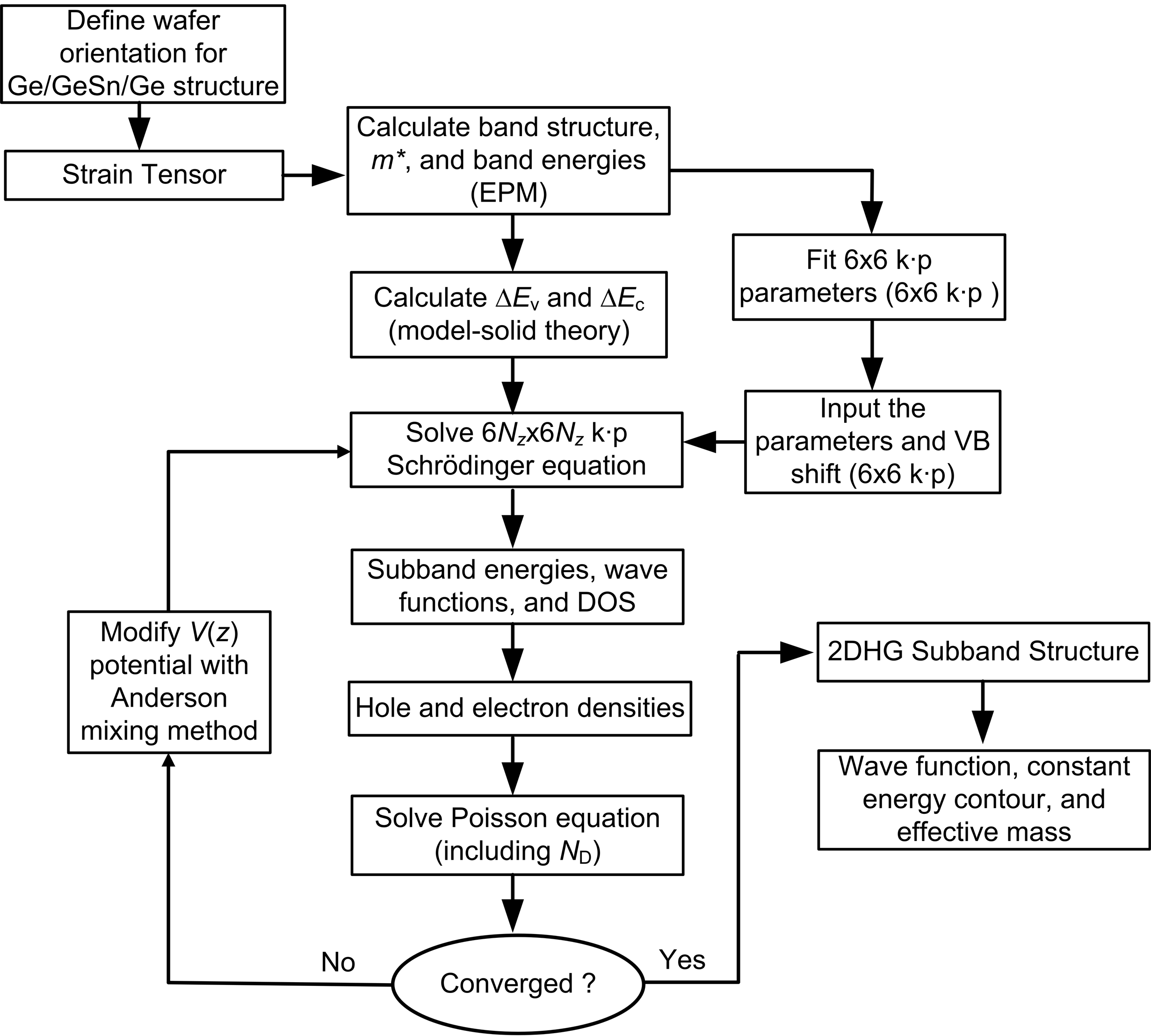
The calculation flowchart in this work is summarized in figure 1. To study valence subband structures in the inversion layer of Ge cap/GeSn QW/Ge pFETs on (001) and (111) Ge substrates, the wafer orientation and the corresponding transferred strain tensor in the crystal coordinate system [15] are determined first. Effective masses (m∗) and valence band structures near the point ( = [0.05 : 0.05] in 2/ unit) along [100], [001], [110], [110], and [111] directions, and band energies at the point of Ge1-xSnx with 0 0.2 under 3, 2, 1, 0, and 1% in-plane biaxial strain on (001), (110), and (111) wafer orientations are calculated using EPM and used to fit 66 kp parameters through the 66 kp model [13, 16]. The fitted 66 kp parameters are obtained by solving nonlinear least squares with the above values calculated by EPM. Note that our EPM [17] has been reported in elsewhere and the calculated bandgaps agree with the experimental data. Linear interpolation of elastic constants (C11, C12, and C44) [18], and a bowing factor of 0.047 Å [19] for the lattice constant () of GeSn alloys are used in the calculations.
| Symbol | Ge | Sn | |
|---|---|---|---|
| Luttinger parameters | 9.4415 | 6.8605 | |
| 2.7433 | 5.8624 | ||
| 3.9298 | 4.3485 | ||
| Deformation potentials (eV) | 2.06 | 2.3 | |
| 7.4608 | 4.1 | ||
| Additional internal strain parameter (eV) | 0.2322 | 2.872 |
The fitted Luttinger parameters (, , and ) and deformation potential parameters ( and ) of Ge and Sn are listed in table 1. The fitted Luttinger parameters of Ge are similar with the previous reported results [20]. To take into account GeSn alloys, the 66 kp parameters are expressed as a quadratic polynomial
| (1) |
where can be , , , or , and the coefficient is a corresponding bowing factor listed in table 2. A linearly interpolated hydrostatic deformation potential for the valence band of GeSn alloys is obtained from reference [21] ( = 2.23 eV and = 1.58 eV). Moreover, for strained Ge1-xSnx (110) and (111) substrates with in-plane biaxial strain, there is a relative displacement of two atoms in the unit cell due to generated shear strains [22, 23]. An additional internal strain parameter () was used in the EPM calculation to take into account the internal strain effects [24]. The used of Ge1-xSnx in EPM is obtained by the linear interpolation of the reported of Ge [22] and Sn [25]. In 66 kp model, the internal strain effect was usually ignored due to few information for parameter correction [14, 26]. To consider the effect in 66 kp model, we use an additional parameter () to modify the fitted deformation potential parameter () of Ge1-xSnx as
| (2) |
where the of Ge1-xSnx is obtained from equation (1), and the fitted of Ge and Sn are listed in table 1.
| Bowing factor | Symbol | GeSn |
|---|---|---|
| Luttinger parameters | 66.6075 | |
| 32.6386 | ||
| 32.8118 | ||
| Deformation potentials (eV) | 0.5502 | |
| 7.906 |
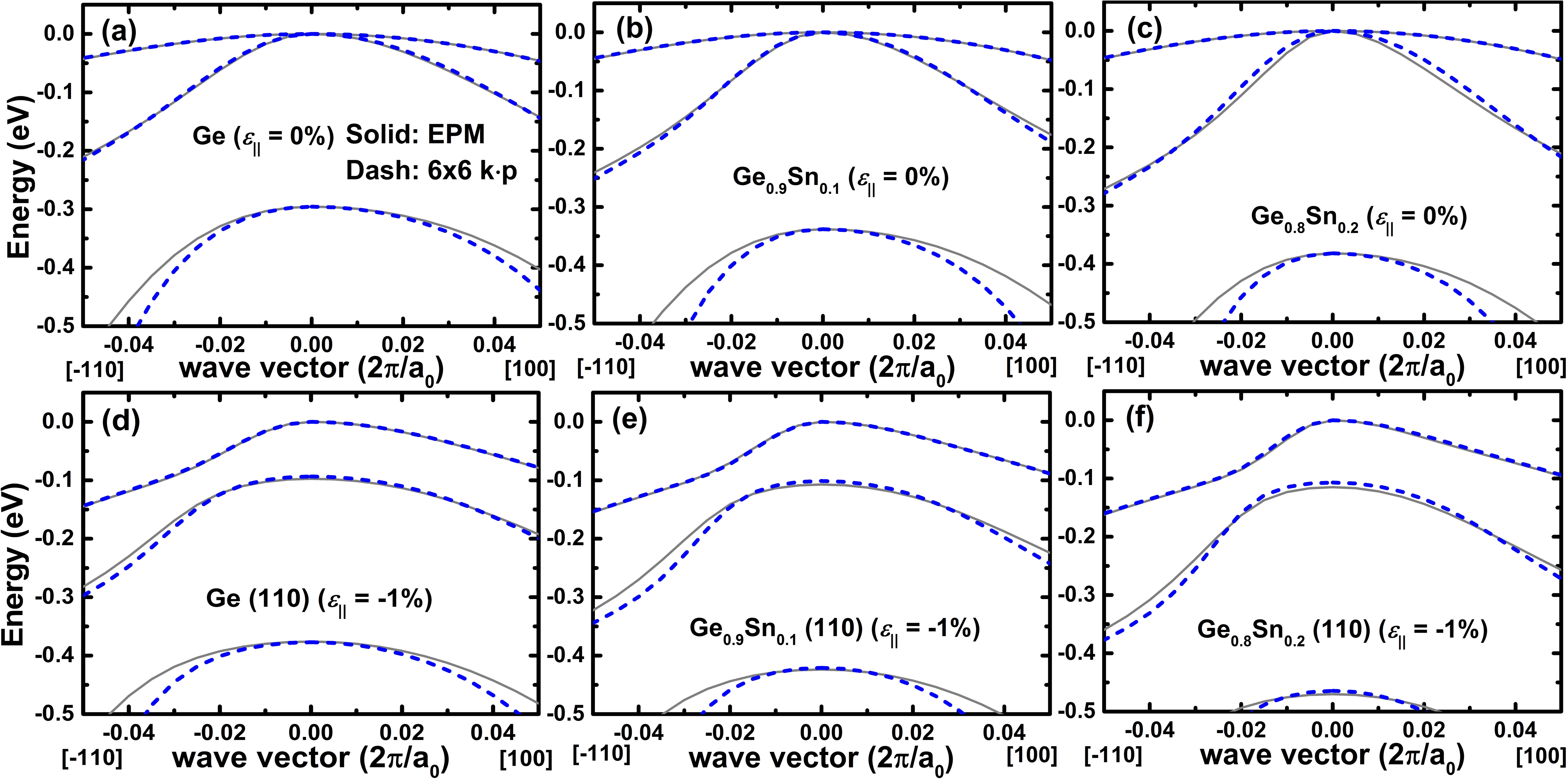
The calculated valence band structures of Ge1-xSnx along [110] and [100] directions with varying Sn content ( = 0, 0.1, and 0.2) and in-plane biaxial compressive strain ( = 0 and 1%) using EPM (solid line) and 66 kp (dashed line) are shown in figure 2. The agreements in band energies between the two methods at the point and two uppermost band structures near the point are presented. The split-off band structure fitting is ignored to obtain best fit of the other two valence bands.
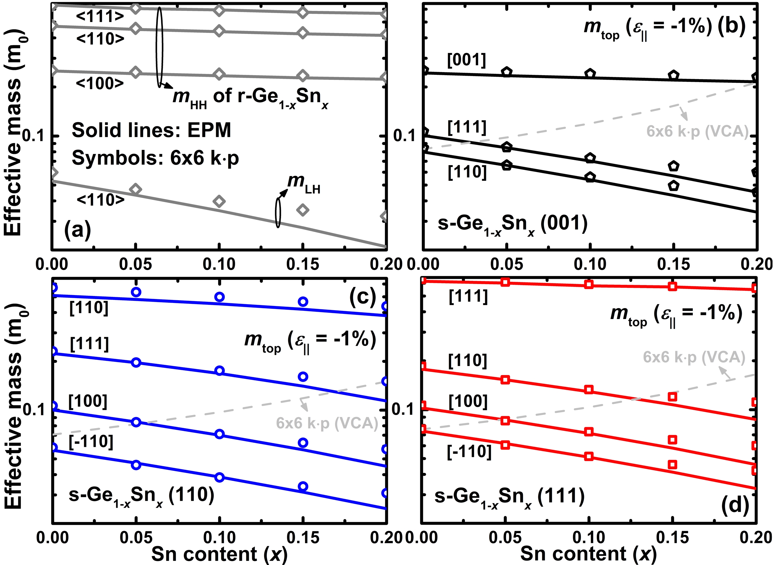
The calculated effective masses of the heavy hole bands () along , , and directions, and light hole bands () along directions of relaxed Ge1-xSnx (r-Ge1-xSnx) alloys using EPM and 66 kp are shown in figure 3(a). The rapid decrease of along direction with increasing for r-Ge1-xSnx is compared against the slow decrease of along , , and directions. In strained Ge1-xSnx (s-Ge1-xSnx) (001) with = 1% (figure 3(b)), the effective masses along [110] and [110] directions are the same due to symmetry of the band structures. For s-Ge1-xSnx (110) and (111) with = 1%, the symmetry is broken by the strain and the top valence band () along [110] direction is smaller than that along [110] (figure 3(c) and (d)). The slow decrease of along the out-of-plane direction in s-Ge1-xSnx (001), (110), and (111) is compared against the rapid decrease of along the other directions. Note that in-plane and out-of-plane directions are usually defined as channel and confined directions, respectively. The calculated by 66 kp based on VCA (dashed lines) along [110], [110], and [110] directions for s-Ge1-xSnx (001) (figure 3(b)), (110) (figure 3(c)), and (111) (figure 3(d)) with = 1%, respectively, are also shown for comparison. The used linearly interpolated 66 kp parameters are adopted from literatures [20, 27, 28].
After fitting 66 kp parameters, the self-consistently calculation between 6 kp Schrödinger and Poisson equations [29, 30] is performed to calculate the two-dimensional hole gas system (2DHG) as shown in figure 1. The denotes mesh points along the confined direction. A uniform mesh of 2 Å size is used. Linear interpolation of dielectric constants of GeSn alloys are used [18]. A valence band offset () at a heterointerface calculated by the model-solid theory (MST) [31, 32] are used to determine the valence band lineup potential in the 6 kp Schrödinger equation. Note that a proposed correction term on the average valence band offset of GeSn alloys [33] is used in MST instead of the linearly interpolated average valence band offset [34]. Our reported calculated of 80 meV in s-Ge0.95Sn0.05/r-Ge by MST [31] is within the reported measurement accuracy range of 50 meV for 0.08 [35]. A duplicate valence band edge (VB) shift in the potential by strain in the 6 kp matrix is removed. The treatment of the 6 kp Hamiltonian matrix at a heterointerface is referred to reference [36]. A 2D density of state (DOS) of each subband is calculated from a tabulation of each subband structure and used to determine the hole density in the inversion layer [37]. The effective mass Schrödinger equations are also performed to calculate the electron density in conduction band heterostructures [38]. A conduction band offset () at a heterointerface is determined by the corresponding bandgaps and . Uniform doping density of 1 cm-3 is used in the Poisson equation [30]. The Anderson mixing method is used to accelerate the convergence of iterative solution [39].
3 Results and Discussion
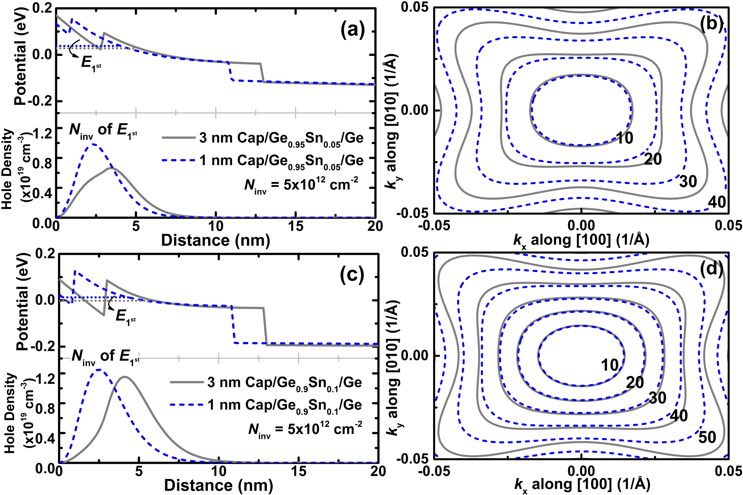
At the total inversion hole density = 5 cm-2, the calculated inversion layers in 3 nm and 1 nm Ge cap/10 nm s-Ge1-xSnx QW on Ge (001) substrate with the first subband hole density distribution are shown in figure 4(a) ( = 0.05) and 4(c) ( = 0.1). The Fermi level energy is fixed at 0 eV in the valence band. The quantized energy of the first subband () crosses the Ge cap and s-Ge1-xSnx QW ( = 0.05 and 0.1) layers. For = 0.05 (figure 4(a)), there is a substantial hole density of in the 3 nm cap as compared to a low hole density of in the 1 nm cap. These hole distributions influence the first subband constant 2D energy contour of the Ge/s-Ge0.95Sn0.05/Ge (001) inversion layer as shown in figure 4(b). Note that the first subband energy dispersion can be expressed as
| (3) |
where is the in-plane vector, is the polar angle in the range [0, /2] from , and is indirectly proportional to / [30, 37]. The energy dispersion is hybridized by the Ge cap and s-Ge0.95Sn0.05 QW. The rapid change in energy (in meV) with increasing for the 1 nm cap is compared against that for the 3 nm cap (figure 4(b)). For = 0.1 (figure 4(c)), the hole density of in the QW layer for the 3 nm and 1 nm cap are similar, which is due to the increase in with increasing . As a result, there is a similar change in energy with increase in for the first subband constant 2D energy contours of the 3 nm and 1 nm cap/s-Ge0.9Sn0.1/Ge (001) inversion layers (figure 4(d)).
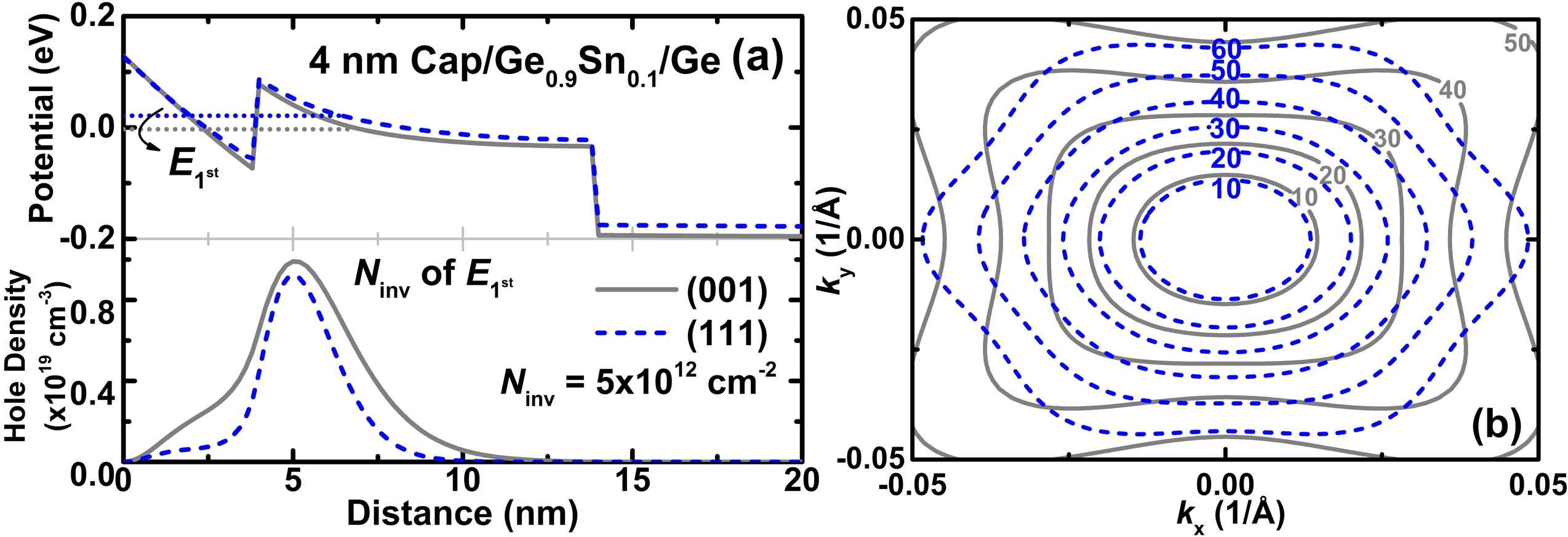
For different orientations, the calculated inversion layers of the 4 nm Ge cap/10 nm s-Ge0.9Sn0.1 QW on Ge (001) and (111) substrates at = 5 cm-2 with the corresponding first subband hole density distribution are shown in figure 5(a). The hole density of in the cap layer for (111) substrate is lower compared to that for (001) in spite of the similar . The of (111) is more confined towards the inside than that of (001), which results in low hole density in the cap layer owing to the larger confined mass of (111) (similar to the out-of-plane values of in figure 3(b) and (d)). The first subband constant 2D energy contours of the Ge/s-Ge0.9Sn0.1/Ge (001) and (111) inversion layers are shown in figure 5(b) for comparison. The in the device coordinate system [15] are [100][010] and [112][110] for (001) and (111), respectively. To study the changes in , at the zone center is calculated using equation (3) with = /4 and /2 for the channel direction/wafer orientation of [110]/(001) and [110]/(111), respectively.
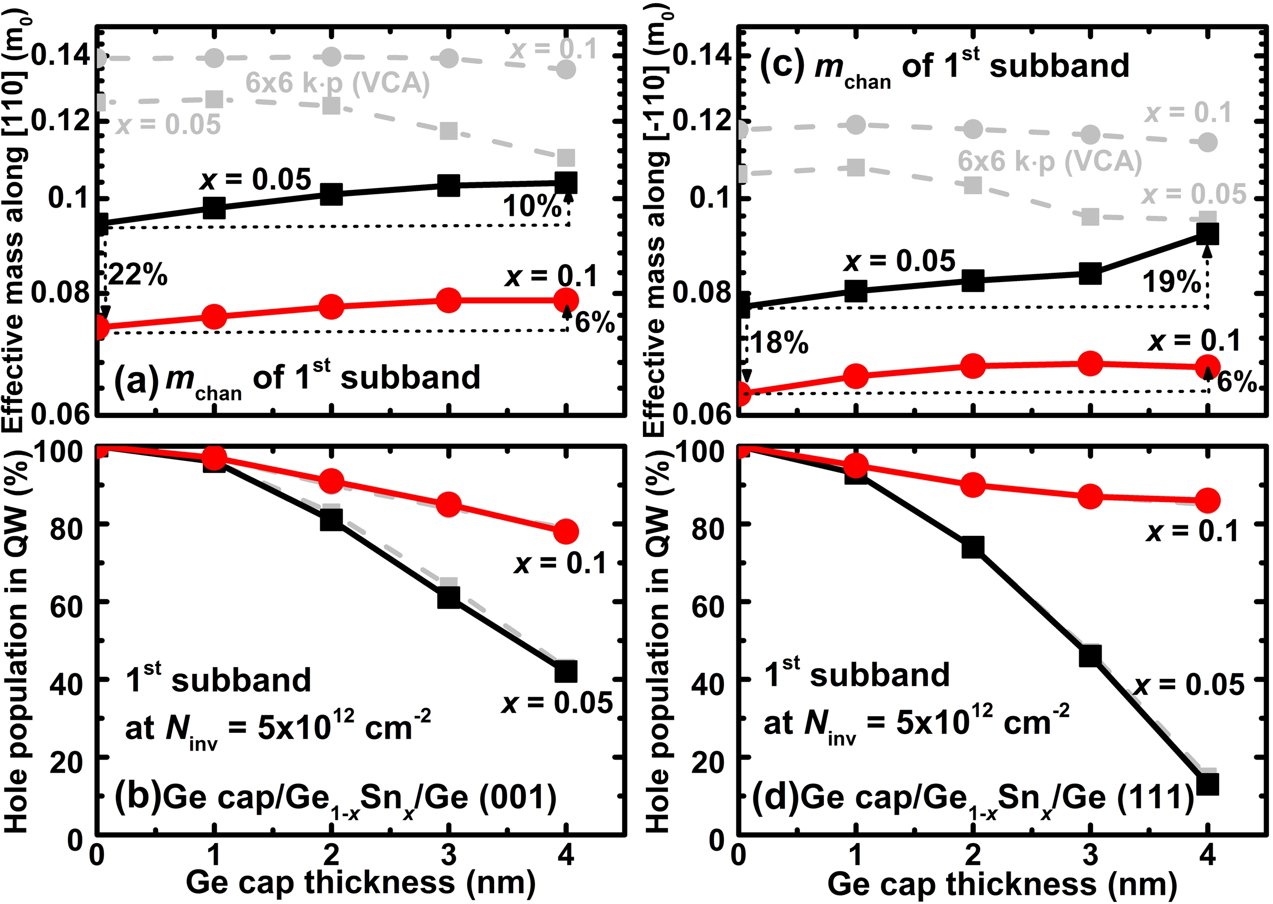
The calculated and hole population in QW as a function of cap thickness of the first subband in the Ge cap/s-Ge1-xSnx ( = 0.05 and 0.1)/Ge (001) and (111) inversion layers at = 5 cm-2 are shown in figure 6. The in the (111) inversion layer (figure 6(c)) is smaller than that in the (001) inversion layer (figure 6(a)) owing to quantum confinement. This is different from the trend seen in bulk effective masses of s-Ge1-xSnx [110]/(001) (figure 3(b)) and [110]/(111) (figure 3(d)). Note that the quantum confinement also causes drastic warped valence subband structures in the case of (110) [40, 41], which is not discussed here. The is reduced with increasing Sn content or decreasing cap thickness. This trend is contrary to the increased calculated by 66 kp (VCA). In the case of 0 nm cap, there is 20% reduction of with an increase of 5% in Sn. The increase in with increasing cap thickness is approximately similar to the increase in the average of in Ge cap and s-Ge1-xSnx QW weighted by its corresponding hole population.
4 Summary
One set of 66 kp Luttinger and deformation potential parameters for valence band structures and effective masses of Ge1-xSnx (001), (110), and (111) wafer orientations, where 0 0.2 with in-plane biaxial strain of 3% 1% are fitted based on the calculated valence band structures by EPM. The internal strain effects by shear strain were taken into account in the EPM and 66 kp calculations. The first valence subband structures in the p-type Ge cap/10 nm s-Ge1-xSnx QW/Ge (001) and (111) inversion layers were theoretically studied using the self-consistent calculation of 6 kp Schrödinger and Poisson equations. The valence band lineups at the heterointerfaces were theoretically determined using the model-solid theory. In the QW structures, the (111) has a lower in the first subband than (001) owing to quantum confinement. The Sn content controls the effective mass and , and the and cap thickness control the hole population in the QW to affect the of the first subband. Using the fitted 66 kp parameters, the increase in Sn content and the decrease in cap thickness reduce the as compared to the incorrect increased using the reported linearly interpolated 66 kp parameters of Ge and Sn.
References
References
- [1] Gallagher J D, Senaratne C L, Kouvetakis J, and Menéndez J 2014 Appl. Phys. Lett. 105 142102
- [2] Costa V R D, Cook C S, Birdwell A G, Littler C L, Canonico M, Zollner S, Kouvetakis J, and Menéndez J 2006 Phys. Rev. B 73 125207
- [3] Wirths S et al 2015 Nature Photon. 9 88
- [4] Low K L, Yang Y, Han G, Fan W, and Yeo Y-C 2012 J. Appl. Phys. 112 103715
- [5] Freitas F L, Furthmüller J, Bechstedt F, Marques M, and Teles L K 2016 Appl. Phys. Lett. 108 092101
- [6] Lan H-S and Liu C W 2014 Appl. Phys. Lett. 104 192101
- [7] Lei D, Wang W, Zhang Z, Pan J, Gong X, Liang G, Tok E-S, and Yeo Y-C 2016 J. Appl. Phys. 119 024502
- [8] Huang Y-S et al 2016 Tech. Dig.-Int. Electron Devices Meet. 33.1.1-33.1.4.
- [9] Zhan C, Wang W, Gong X, Guo P, Liu B, Yang Y, Han G, and Yeo Y-C 2013 Int. Symp. VLSI Technol. Syst. Appl. (VLSI-TSA) 82-83.
- [10] Liu Y et al 2014 Semicond. Sci. Technol. 29 115027
- [11] Liu M, Han G, Liu Y, Zhang C, Wang H, Li X, Zhang J, Cheng B, and Hao Y 2014 Symp. VLSI Technol., Dig. Tech. Pap. 80-81.
- [12] Gupta S, Huang Y-C, Kim Y, Sanchez E, and Saraswat K C 2013 IEEE Electron Device Lett. 34(7) 831
- [13] Chang S-T, Fan J W, Lin C-Y, Cho T-C, and Huang M 2012 J. Appl. Phys. 111 033712
- [14] Pham A-T, Jungemann C, and Meinerzhagen B 2007 IEEE Trans. Electron Devices 54 2174
- [15] Rahman A, Lundstrom M S, and Ghosh A W 2005 J. Appl. Phys. 97 053702
- [16] Chuang S L, ”Physics of Optoelectronic Devices”. 1995: John Wiley sons, New York.
- [17] Lan H-S, Chang S T, and Liu C W 2016 Semiconductor, topological semimetal, indirect semimetal, and topological Dirac semimetal phases of Ge1-xSnx alloys Preprint arXiv:1612.00159
- [18] Chang G-E, Chang S-W, and Chuang S L 2010 IEEE J. Quantum Electron. 46(12) 1813
- [19] Beeler R, Roucka R, Chizmeshya A V G, Kouvetakis J, and Menéndez J 2011 Phys. Rev. B 84 035204
- [20] Rideau D, Feraille M, Ciampolini L, Minondo M, Tavernier C, and Jaouen H 2006 Phys. Rev. B 74 195208
- [21] Li Y-H, Gong X G, and Wei S-H 2006 Phys. Rev. B 73 245206
- [22] Walle C G V d and Martin R M 1986 Phys. Rev. B 34 5621
- [23] Ungersboeck E, Gös W, Dhar S, Kosina H, and Selberherr S 2008 Math. Comput. Simulat. 79 1071-1077
- [24] Ungersboeck E, Dhar S, Karlowatz G, Sverdlov V, Kosina H, and Siegfried Selberherr 2007 IEEE Trans. Electron Devices, 54 2183
- [25] Molinas-Mata P, Shields A J, and Cardona M 1993 Phys. Rev. B 47 1866
- [26] Wang E X, Matagne P, Shifren L, Obradovic B, Kotlyar R, Cea S, Stettler M, and Giles M D 2006 IEEE Trans. Electron Devices 53(8) 1840
- [27] Lawaetz P 1971 Phys. Rev. B 4(10) 3460
- [28] Moontragoon P, Vukmirović N, Ikonić Z, and Harrison P 2008 J. Appl. Phys. 103 103712
- [29] Lan H-S, Chen Y-T, Lin J-Y, and Liu C W 2013 ECS Trans. 50 151-155
- [30] Zhang Y, Fischetti M V, Sorée B, Magnus W, Heyns M, and Meuris M 2009 J. Appl. Phys. 106 083704
- [31] Lan H-S and Liu C W 2017 J. Phys. D: Appl. Phys. 50 13LT02
- [32] Walle C G V d 1989 Phys. Rev. B 39 1871
- [33] Senaratne C L, Wallace P M, Gallagher J D, Sims P E, Kouvetakis J, and Menéndez J 2016 J. Appl. Phys. 120 025701
- [34] Lan H-S and Liu C W 2016 ECS Transactions 75 571-578
- [35] Chou H-Y et al 2014 Appl. Phys. Lett. 104 202107
- [36] Liu Y X, Ting D Z-Y, and McGill T C 1996 Phys. Rev. B 54 5675
- [37] Fischetti M V, Ren Z, Solomon P M, Yang M, and Rim K 2003 J. Appl. Phys. 94 1079
- [38] Lan H-S, Chen Y-T, Hsu W, Chang H-C, Lin J-Y, Chang W-C, and Liu C W 2011 Appl. Phys. Lett. 99 112109
- [39] Eyert V 1996 J. Comput. Phys. 124 271-285
- [40] Hsieh B-F and Chang S-T 2011 Solid-State Electron. 60 37-41
- [41] Sun G, Sun Y, Nishida T, and Thompson S E 2007 J. Appl. Phys. 102 084501