Creation of Half-metallic -orbital Dirac Fermion with Superlight Elements in Orbital-Designed Molecular Lattice
Abstract
Magnetism in solids generally originates from the localized - or -orbitals that are hosted by heavy transition-metal elements. Here, we demonstrate a novel mechanism for designing half-metallic -orbital Dirac fermion from superlight -elements. Combining first-principles and model calculations, we show that bare and flat-band-sandwiched (FBS) Dirac bands can be created when C20 molecules are deposited into a 2D hexagonal lattice, which are composed of -molecular orbitals (MOs) derived from -atomic orbitals (AOs). Furthermore, charge doping of the FBS Dirac bands induces spontaneous spin-polarization, converting the system into a half-metallic Dirac state. Based on this discovery, a model of spin field effect transistor is proposed to generate and transport 100% spin-polarized carriers. Our finding illustrates a novel concept to realize exotic quantum states by manipulating MOs, instead of AOs, in orbital-designed molecular crystal lattices.
keywords:
half-metallic semimetal, fullerene, superatom, -orbitals, tight-bindingDepartment of Materials Science and Engineering, University of Utah, Salt Lake City, UT 84112, USA \alsoaffiliationDepartment of Materials Science and Engineering, University of Utah, Salt Lake City, UT 84112, USA \alsoaffiliationDepartment of Materials Science and Engineering, University of Utah, Salt Lake City, UT 84112, USA \alsoaffiliationDepartment of Physics, Jining University, Qufu 273155, China \alsoaffiliationCollaborative Innovation Center of Quantum Matter, Beijing 100084, China \abbreviationsC20,TB,SpinFET
Magnetic ordering in solids is generally associated with heavy elements, and tremendous efforts have been devoted to finding transition metal (TM) based ferromagnetic (FM) materials1, 2 for spintronic device applications in the past decades. It has been known for a long time, according to Stoner criterion3, that the origin of FM order in solids arises from the partially occupied (localized) - or -orbitals, which gives rise to a significantly large density of state (DOS) at Fermi level (), and drive the system into a FM ground state. Half-metal4, 5, with a 100% spin-polarized FM state, i.e., conducting in one spin channel and insulating in the other, is an ideal candidate6 for spin injection and filtering. However, half-metals are very rare and only three-dimensional (3D) Heusler compounds7, 8, binary metal oxides CrO29 and mixed valence perovskites10 have been identified as half-metals in experiments.
Unfortunately, the strong spin scattering induced by the large spin-orbit coupling (SOC) of heavy elements may significantly reduce the spin relaxation time and mean free path during spin transport. As a result, great attention has been attracted to searching for -electron magnetism in place of - or - electron magnetism. Local FM order and even half-metallic state have been predicted and confirmed to exist in graphene-related 2D systems, some involving local defects or impurities11, 12, 13, 14, 15, 16. However, the realization of local magnetic states in graphene-related systems requires either large external electric fields or well-ordered defects/dopants. It is therefore highly desirable to discover new mechanisms for realizing delocalized FM states in -electron systems beyond the graphene models.
In this Communication, we demonstrate a novel concept for designing homogenous and long-range magnetism in an -electron molecular crystal. Our design principle is twofold: first, beyond atomic crystals, molecular crystals are proposed to form with pre-defined lattice symmetries by taking the advantages of chemical synthesis and epitaxial growth17, 18, 19, 20, 21, 22; second, overcoming the fixed orbital energy sequence of atomic orbitals (AOs), molecular orbitals (MOs) having different orbital energy and sequences are designed to have artificial frontier orbitals with large angular momenta (e.g. and ) in a given crystal field to exhibit exotic quantum features, including magnetism23.
Specifically, we illustrate this novel design concept by first-principles and model calculations which show the existence of a half-metallic Dirac semimetal state in 2D molecular crystals made of fullerenes. Taking C20 molecules as an example, once these “superatoms” are arranged into a hexagonal lattice, our first-principles calculations show that the frontier -MOs form bare and flat-band-sandwiched (FBS) Dirac bands around the band gap of the 2D-C20 layer. Interestingly, additional fractional charge doping induces a spontaneous spin-polarization of FBS Dirac bands, giving rise to a half-metallic Dirac semimetal state. For potential device applications, the mechanism of our findings can be applied to design a spin field effect transistor (SFET) built from the 2D-C20 layer, to generate and transport 100% spin-polarized carriers.
All the first-principles density functional theory (DFT) calculations are performed using the plane-wave basis Vienna ab initio simulation package (VASP)24, 25 with Perdew-Burke-Ernzerhof exchange correlation functional26. The cutoff energy for plane wave is chosen to be 400 eV and the vacuum space is set to 15 Å. All the atoms in the unit cell are relaxed until the forces are smaller than 0.01 eV/Å. Our test calculations show that SOC has a negligible effect on the electronic properties of C20 systems. The DFT results are used as input to construct the maximally localized Wannier funcitons (MLWFs) with the WANNIER90 code27. The MOs of single C20 molecule is calculated using Gaussian09 package at b3lyp/6-31g level. The charge conductance of 2D-C20 layer are calculated using the DFT non-equilibrium Green’s Function method, as implemented in Atomistix ToolKit (ATK) package.
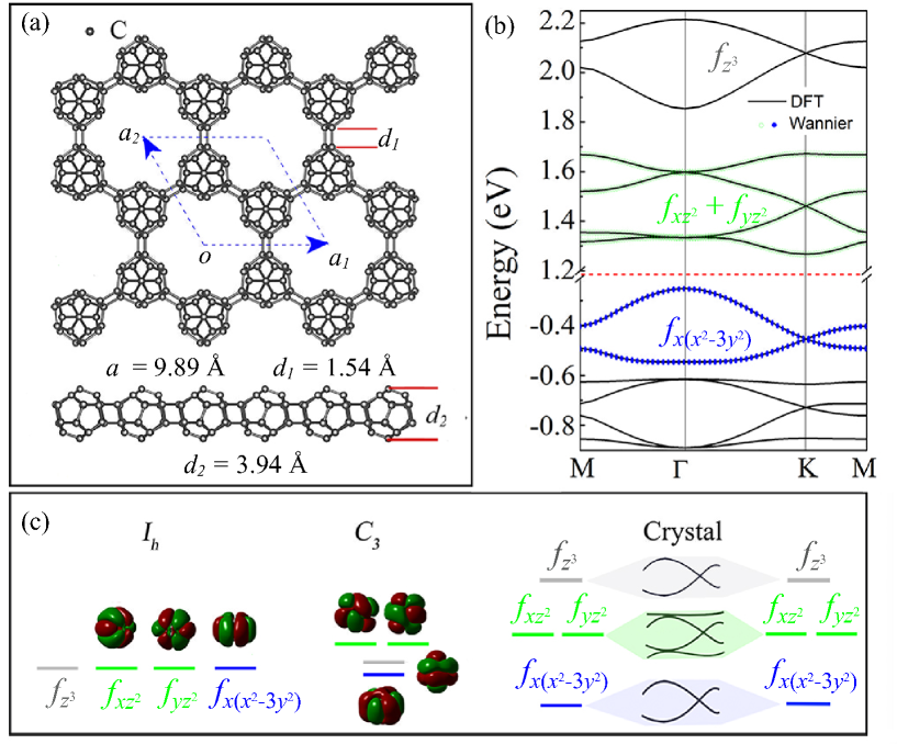
The C20 molecule, which was first synthesized in 200028, is known as the smallest fullerene, and it has a dodecahedral cage structure. Important for our purpose, C20 molecules can form molecular crystals with various structural symmetries, such as hexagonal and fcc crystals18, 19. When C20 molecules are constrained into a 2D lattice, our extensive structural searches based on DFT calculations confirm that the hexagonal lattice is the most stable one, as shown in Figure 1a. In this structure, two single C-C bonds ( Å) between the neighboring C20 molecules are formed. The calculated equilibrium lattice constant is Å and thickness Å.
Figure 1b shows the calculated band structure of 2D-C20 lattice. It is a nonmagnetic (NM) semiconductor with an indirect band gap of 1.5 eV. Two subsets of bare Dirac bands and two subsets of FBS Dirac bands appear around the band gap. These Dirac bands appear in different energy ranges without overlapping, and the lies in the gap between two sets of bare and FBS Dirac bands. As we learned from graphene models, the appearance of bare (FBS) Dirac bands could be a result of single (double ) orbital hopping on a hexagonal lattice29, 30, 31, 32. However, in our C20 system all the -AOs from forty C atoms (per unitcell) contribute to the formation of these Dirac bands and flat bands, as shown in Figure S133. Thus, it is impossible to understand these Dirac bands by the simple single- or double-AO hopping mechanism developed in graphene models.
Individual C20 “superatom” has a symmetry in its gas phase (C), and its MOs are arranged in the order of 34 based on Gaussian09 calculations, as shown in Figure S233, which is significantly different from that of single C atom. Based on electron counting, the four degenerated highest occupied MOs (HOMOs) are of -type and occupied by two electrons, as shown in Figure 1c (left panel). When C20 molecules are arranged into a hexagonal lattice, these -MOs are splitted into two single and orbitals plus one double-degenerated orbital according to crystal field symmetry, as shown in Figure 1c (middle panel). From orbital symmetry analysis, one finds that the or () orbital has a similar in-plane symmetry as the () orbital in a hexagonal lattice. It is, therefore, reasonable to expect that hopping between or () orbitals will share similar features as that of () orbitals. Indeed, our Wannier function calculations show that one (two) MLWF orbital(s) of or (), located at the center of the carbon cage, can be uniquely applied to fit perfectly the bare (FBS) Dirac bands around the , confirming our physical intuition (right panel of Figure 1c).
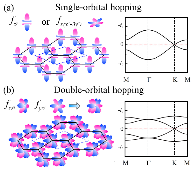
In order to have a more general understanding of the formation of bare and FBS -orbital Dirac bands, as discovered in the 2D-C20 layer, we further develop a single- and double-MO hopping mechanism based on a nearest neighbor (NN) hopping tight-binding (TB) model, as shown in Figure 2. Here, the general set of -orbital based Slater-Koster hopping integrals35 are adopted, and a () matrix is constructed to describe the two-band (four-band) single- (double-) () orbital hopping in a hexagonal lattice, which can be written as:
| (1) |
For simplicity, the on-site energies are set to zero (), and the off-diagonal terms capture the NN hoppings. For the single-orbital case [ is similar to ], the hopping integral can be described as . For the double-orbital case, the hopping integrals can be described as:
| (2) |
where , , and . Here, , , and Because of the f-orbital angular momentum having , we have four basic hopping terms, i.e., , , and . In our calculation, the values of these four hopping terms are set to , , , and (in unit of ), respectively. After the diagonalization of Eq. (1), we obtain two-band and four-band band structures, respectively, as shown in Figs. 2a and 2b (right panel). Our simple TB models can faithfully reproduce both bare and FBS Dirac bands as obtained from DFT calculations (Figure 1b). The main features of bare and FBS Dirac bands are insensitive to the detailed values of hopping parameters (except for the slight variation of band dispersion and widths), indicating that they are very robust and generally exist in many -orbital systems with similar lattice symmetry.
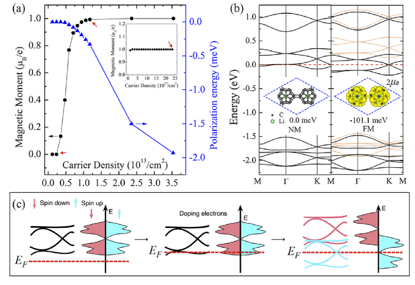
It is important to note that the nontrivial flat band created in 2D-C20 layer (wavefunction is delocalized in real space) is significantly different from that created by defects in semiconductors (wavefunction is localized in real space).This unusual flat band at the bottom of the conduction band indicates that a small perturbation of exchange interaction introduced by carrier (electron) doping can induce a large spin splitting, because of the very nature of flat band with an “infinitly” large DOS36. Accordingly, the critical value of carrier concentration () for spontaneous spin-polarization in 2D-C20 system may be much smaller than that in conventional FM materials, according to Stoner criterion. To confirm this expectation, we have calculated the magnetic moment of the system as a function of and the spin-polarization energy (the energy difference between spin-polarized ground state and spin-unpolarized state), which is shown in Figure 3a. When increases, the flat band becomes partially occupied and the DOS at increases quickly. The critical for spin-polarization in the 2D-C20 lattice is estimated to be as small as marked by the left red arrow, which could be achieved in the current experiments by gating (order of )37, 38. When , the magnetic moment (black circles) continues to increase with the increasing , while the spin-polarization energy decreases (blue triangles). Once marked by the middle red arrow, the magnetic moment saturates at , as shown in the inset of Figure 3a, and the system becomes a half-metal, and the corresponding band structure is shown in Figure S333.
Another effective approach to doping of a C20 molecule is to encapsulate alkali atoms into the cage of fullerene, which has been achieved in the experiments39, 40. Taking Li as a protoypical example, we insert one Li atom into each C20 cage to form a 2D-Li@C20 layer, as shown in the inset of Figure 3b. Overall, the equilibrium geometry and lattice parameters of 2D-C20 layer change very little after Li doping. When spin-polarization is excluded (NM case), the calculated band structure is almost the same as the undoped case, except for the shift of to the contacting region between the Dirac bands and the flat band. Including spin-polarization, the half-metallic ground state (right panel of Figure 3b) is energetically more favorable than the NM state by about 101.1 meV per unitcell. Interestingly, the locates exactly at the Dirac point of the majority (spin-up) channel, creating a half-metallic Dirac semimetal phase with a eV half-metallic gap, and the is , marked by a red arrow in the inset of Figure 3a. The Fermi velocity of 2D-Li@C20 is estimated to be m/s, close to that of graphene.
The above findings demonstrate an attractive mechanism for realizing half-metallic Dirac semimetal state by manipulating the MOs of fullerene. First, C20 molecule, which has a degenerate -MOs at HOMO, can be used to generate FBS Dirac bands at the bottom of conduction band under specific crystal field splitting (left panel of Figure 3c). Second, small “finite” (fractional) charge doping of the flat band will induce a large spin-polarization, because of its “infinitely” large DOS. As a result, the system is converted from a NM (middle panel of Figure 3c) to a half-metallic ground state (right panel of Figure 3c). Especially, a half-metallic Dirac fermion state can be achieved by a critical by gating or monolayer decoration of alkali atoms.
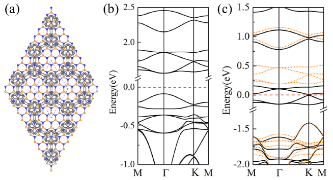
In practice, the growth of fullerene monolayer with controllable lattice symmetries could be achieved by selection of specific substrates18, 19. Hexagonal BN (-BN) has been widely selected as an ideal substrate to grow various 2D materials by van de Waals (vdW) epitaxy. Using -BN as a candidate substrate, our structure search shows that 2D-C20 (or 2D-Li@C20) can perfectly fit a -BN supercell (lattice mismatch is smaller than 1%), as shown in Fig. 4a. Combing the vdW corrections with DFT, the optimized structure of 2D-C20 on -BN is shown in Fig. 4a (the structure of 2D-Li@C20 on -BN is similar and not shown here). The minimal distance between C20 and the -BN is around 3.2 Å, indicating a weak interfacial interaction. Our band structure calculations have confirmed that the basic electronic structural characteristics of 2D-C20 (-orbtial Dirac bands around bottom of conduction band and top of valence band, as shown in Fig. 4b) and 2D-Li@C20 (half-metallic Dirac band across the Fermi level, as shown in Fig. 4c) maintain on -BN substrate. Besides -BN, it is expected that 2D-C20 could also be grown on other insulating substrates where its exciting electronic structures can be maintained.
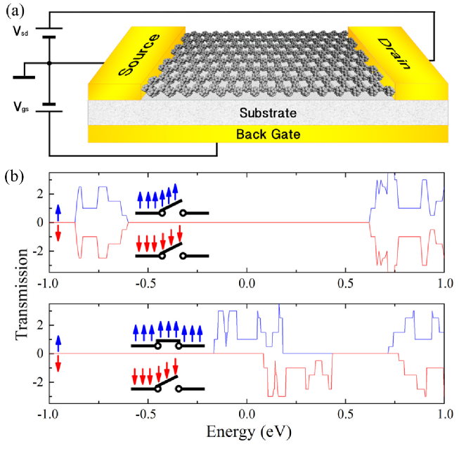
Once the hexagonal lattice of C20 monolayer is grown on a insulating substrate with weak interaction, e.g., the case of C20 on -BN, then a 2D-C20 based SFET model device can be made, as shown in Figure 5a. Without gate voltage (=0), the 2D-C20 monolayer is NM semiconducting with a band gap of eV. Thus, a conductance gap exists around the (OFF status), as shown in Figure 5b (upper panel). To overcome this transport gap, a bias voltage V has to be applied to drive the spin-unpolarized charge flow through the 2D-C20 layer. When the is applied larger than a threshold to achieve the critical doping to occupy the conduction flat band. The system is converted into a half-metallic state (ON status), as shown in Figure 5b (bottom panel). In this configuration, a small is able to drive a 100% spin-polarized current through the 2D-C20 monolayer. Furthermore, a proper induced charge doping can convert the system into a half-metallic Dirac semimetal state, in which the carriers with 100% spin-polarization will transport with ultrafast speed.
In conclusion, we demonstrate a novel mechanism for achieving a half-metallic Dirac semimetal state from the manipulation of MOs of fullerenes, by designing large-angular-momentum (- and -) frontier MOs from linear combination of small-angular-momentum (- and -) AOs. Our discovery opens an new avenue to realizing exotic quantum states from orbital-designed molecular crystal lattices.
B.C. acknowledges the support from NSFC and China Scholarship Council (Grant No. 11404188 and 201406225022). B.H., K.J., W.J., and F.L. acknowledge the support from DOE-BES (Grant No. DE-FG02-04ER46148). B.H. also acknowledges the support from NSFC (Grant No.: 11574024) and NSAF U1530401. We thank the CHPC at the University of Utah for providing the computing resources.
References
- 1 T. Dietl and H. Ohno, Rev. Mod. Phys. 86, 187 (2014).
- 2 S. A. Wolf, Science 294, 1488 (2001).
- 3 E. C. Stoner, Proc. R. Soc. London, Ser. A 165, 372 (1938).
- 4 R. A. de Groot, F. M. Mueller, P. G. van Engen, and K. H. J. Buschow, Phys. Rev. Lett. 50, 2024 (1983).
- 5 H. van Leuken and R. A. de Groot, Phys. Rev. Lett. 74, 1171 (1995).
- 6 F. J. Jedema, A. T. Filip, and B. J. van Wees, Nature 410, 345 (2001).
- 7 J. W. Dong, L. C. Chen, C. J. Palmstrom, R. D. James, and S. McKernan, Appl. Phys. Lett. 75, 1443 (1999).
- 8 M. Jourdan, J. Minár, J. Braun, A. Kronenberg, S. Chadov, B. Balke, A. Gloskovskii, M. Kolbe, H. J. Elmers, G. Schönhense, H. Ebert, C. Felser, and M. Kläui, Nat. Commun. 5, 3974 (2014).
- 9 S. M. Watts, S. Wirth, S. von Molnár, A. Barry, and J. M. D. Coey, Phys. Rev. B 61, 9621 (2000).
- 10 J.-H. Park, E. Vescovo, H.-J. Kim, C. Kwon, R. Ramesh, and T. Venkatesan, Nature 392, 794 (1998).
- 11 M. Fujita, K. Wakabayashi, K. Nakada, and K. Kusakabe, J. Phys. Soc. Japan 65, 1920 (1996).
- 12 Y.-W. Son, M. L. Cohen, and S. G. Louie, Nature 444, 347 (2006).
- 13 T. B. Martins, R. H. Miwa, A. J. R. da Silva, and A. Fazzio, Phys. Rev. Lett. 98, 196803 (2007).
- 14 E.-j. Kan, Z. Li, J. Yang, and J. G. Hou, J. Am. Chem. Soc. 130, 4224 (2008).
- 15 P. Esquinazi, D. Spemann, R. H hne, A. Setzer, K.-H. Han, and T. Butz, Phys. Rev. Lett. 91, 227201 (2003).
- 16 G. Z. Magda, X. Jin, I. Hagymasi, P. Vancso, Z. Osvath, P. Nemes-Incze, C. Hwang, L. P. Biro, and L. Tapaszto, Nature 514, 608 (2014).
- 17 N. Stock and S. Biswas, Chem. Rev. 112, 933 (2012).
- 18 Z. Wang, X. Ke, Z. Zhu, F. Zhu, M. Ruan, H. Chen, R. Huang, and L. Zheng, Phys. Lett. A 280, 351 (2001).
- 19 Z. Iqbal, Y. Zhang, H. Grebel, S. Vijayalakshmi, A. Lahamer, G. Benedek, M. Bernasconi, J. Cariboni, I. Spagnolatti, R. Sharma, F. J. Owens, M.E.Kozlov, K. V. Rao, and M. Muhammed, Eur. Phys. J. B 31, 509 (2003).
- 20 X. Roy, C.-H. Lee, A. C. Crowther, C. L. Schenck, T. Besara, R. A. Lalancette, T. Siegrist, P. W. Stephens, L. E. Brus, P. Kim, et al., Science 341, 157 (2013).
- 21 J. Plas, O. Ivasenko, N. Martsinovich, M. Lackinger, and S. De Feyter, Chem. Comm. 52, 68 (2016).
- 22 L. A. Rochford, T. S. Jones, and C. B. Nielsen, J. Phys. Chem. Lett. 7, 3487 (2016).
- 23 D. A. Tomalia and S. N. Khanna, Chem. Rev. 116, 2705 (2016).
- 24 G. Kresse and J. Furthmüller, Computational Materials Science 6, 15 (1996).
- 25 G. Kresse and J. Furthmüller, Phys. Rev. B 54, 11169 (1996).
- 26 J. P. Perdew, K. Burke, and M. Ernzerhof, Phys. Rev. Lett. 77, 3865 (1996).
- 27 A. A. Mostofi, J. R.Yates,Y. S. Lee, I. Souza, D.Vanderbilt, and N. Marzari, Comput. Phys. Commun. 178, 685 (2008).
- 28 H. Prinzbach, A. Weiler, P. Landenberger, F. Wahl, J. Worth, L. T. Scott, M. Gelmont, D. Olevano, and B. v. Issendorff, Nature 407, 60 (2000).
- 29 P. R. Wallace, Phys. Rev. 71, 622 (1947).
- 30 S. Reich, J. Maultzsch, C. Thomsen, and P. Ordejón, Phys. Rev. B 66, 035412 (2002).
- 31 C. Wu, D. Bergman, L. Balents, and S. Das Sarma, Phys. Rev. Lett. 99, 070401 (2007).
- 32 Z. Liu, Z.-F. Wang, J.-W. Mei, Y.-S. Wu, and F. Liu, Phys. Rev. Lett. 110, 106804 (2013).
- 33 Supporting Materials.
- 34 A. V Verkhovtsev, R. G. Polozkov, V. K. Ivanov, A. V Korol, and A. V Solov’yov, J. Phys. B At. Mol. Opt. Phys. 45, 215101 (2012).
- 35 J. C. Slater and G. F. Koster, Phys. Rev. 94, 1498 (1954).
- 36 Z. Liu, F. Liu, and Y.-S. Wu, Chinese Phys. B 23, 77308 (2014).
- 37 B. Radisavljevic, A. Radenovic, J. Brivio, V. Giacometti, and A. Kis, Nat. Nanotechnol. 6, 147 (2011).
- 38 T. Roy, M. Tosun, X. Cao, H. Fang, D.-H. Lien, P. Zhao, Y.-Z. Chen, Y.-L. Chueh, J. Guo, and A. Javey, ACS Nano 9, 2071 (2015).
- 39 J. R. Heath, S. C. O’Brien, Q. Zhang, Y. Liu, R. F. Curl, F. K. Tittel, and R. E. Smalley, J. Am. Chem. Soc. 107, 7779 (1985).
- 40 S. Aoyagi, E. Nishibori, H. Sawa, K. Sugimoto, M. Takata, Y. Miyata, R. Kitaura, H. Shinohara, H. Okada, T. Sakai, Y. Ono, K. Kawachi, K. Yokoo, S. Ono, K. Omote, Y. Kasama, S. Ishikawa, T. Komuro, and H. Tobita, Nat. Chem. 2, 678 (2010).
This will usually read something like: “Experimental procedures and characterization data for all new compounds. The class will automatically add a sentence pointing to the information on-line: