High quality atomically thin PtSe2 films grown by molecular beam epitaxy 111The authors declare no competing financial interest.
Abstract
Atomically thin PtSe2 films have attracted extensive research interests for potential applications in high-speed electronics, spintronics and photodetectors. Obtaining high quality, single crystalline thin films with large size is critical. Here we report the first successful layer-by-layer growth of high quality PtSe2 films by molecular beam epitaxy. Atomically thin films from 1 ML to 22 ML have been grown and characterized by low-energy electron diffraction, Raman spectroscopy and X-ray photoemission spectroscopy. Moreover, a systematic thickness dependent study of the electronic structure is revealed by angle-resolved photoemission spectroscopy (ARPES), and helical spin texture is revealed by spin-ARPES. Our work provides new opportunities for growing large size single crystalline films for investigating the physical properties and potential applications of PtSe2.
keywords:
PtSe2, Molecular beam epitaxy (MBE), Raman, ARPES, Transition metal dichalcogenide (TMDC)Collaborative Innovation Center of Quantum Matter, Beijing, China \alsoaffiliationCollaborative Innovation Center of Quantum Matter, Beijing, China \alsoaffiliationCollaborative Innovation Center of Quantum Matter, Beijing, China \phone+86 010 62797928
Layered transition metal dichalcogenides (TMDCs) have attracted extensive interests for applications in electronics, optoelectronics and valleytronics due to the strong spin-orbit coupling, sizable band gap and tunability of the electronic structure by quantum confinement effect. 1, 2, 3, 4 In the past decade, this has been witnessed by the significant efforts conducted on the atomically thin MoS2 film. 5, 6, 7 However, its low mobility has limited applications, for inbstance, in high speed electronics. 8, 9 Finding thin films of other TMDC with better properties is highly desirable. PtSe2 has emerged as an interesting compound that belongs to TMDC. Although the bulk crystal is a semimetal, 10, 11 monolayer (ML) platinum diselenide (PtSe2) has been revealed to be a semiconductor with a band gap of 1.2 eV. 12 Importantly, the charge-carrier mobility of PtSe2 has been predicted among the highest in TMDCs 9 and has been experimentally shown to be comparable to black phosphorene 13 yet with the advantage of much improved stability. 14 This makes PtSe2 a promising candidate for high-speed electronics. Moreover, the hidden helical spin texture with spin-layer locking in monolayer PtSe2 has been recently revealed, 15 and such spin physics induced by a local Rashba effect has great potential for electric field tunable spintronic devices. 16. In addition, remarkable performance for photocatalytic activity, 12, 17, 18, 19 photodetection 20 and quick-response gas sensing 21 has also been demonstrated. Therefore, PtSe2 is an attractive candidate for a variety of applications. Obtaining high quality PtSe2 films is a critical step toward this goal.
Monolayer PtSe2 film has been first grown by direct selenization of Pt(111) substrate,12 which is convenient to yield large films up to millimeter size. However, growing such film on metallic Pt substrates hinders the electronics application which instead requires an insulating substrate. The direct selenization method results in a self-terminating monolayer thin film, while thicker films cannot be grown using this method. Although atomically thin PtSe2 flakes with different thickness can mechanically exfoliated from the bulk crystals, 14 the sample size is still unsatisfactory and unscalable. Recently, the attempts of growing PtSe2 films by either chemical vapor deposition (CVD) 22, 23 or thermally assisted conversion (TAC). 24 are reported, however, the polycrystalline nature and lack of atomic-level thickness control are yet to be improved. On the other hand, molecular beam epitaxy (MBE) can provide a better control in terms of growth dynamics and realization of large size, high quality single crystalline films on various substrates with controlled film thickness, 25, 26 thus providing important material basis for investigating the physical properties and potential applications. In this work, we report the first layer-by-layer growth of high quality epitaxial PtSe2 thin films on bilayer graphene/6H-SiC (0001) substrate. The growth process is monitored by reflection high-energy electron diffraction (RHEED) and low-energy electron diffraction (LEED). The high sample quality is revealed by atomic force microscopy (AFM) measurements. We present a systematic study of the vibrational modes and core levels as a function of film thickness by Raman spectroscopy and X-ray photoemission spectroscopy (XPS). Moreover, the band structure measured by angle-resolved photoemission spectroscopy (ARPES) from 1 ML to 22 ML PtSe2 thin films shows the shrinking of band gap as the film thickness increases. Spin-ARPES measurements further reveal the helical spin texture with spin-layer locking.
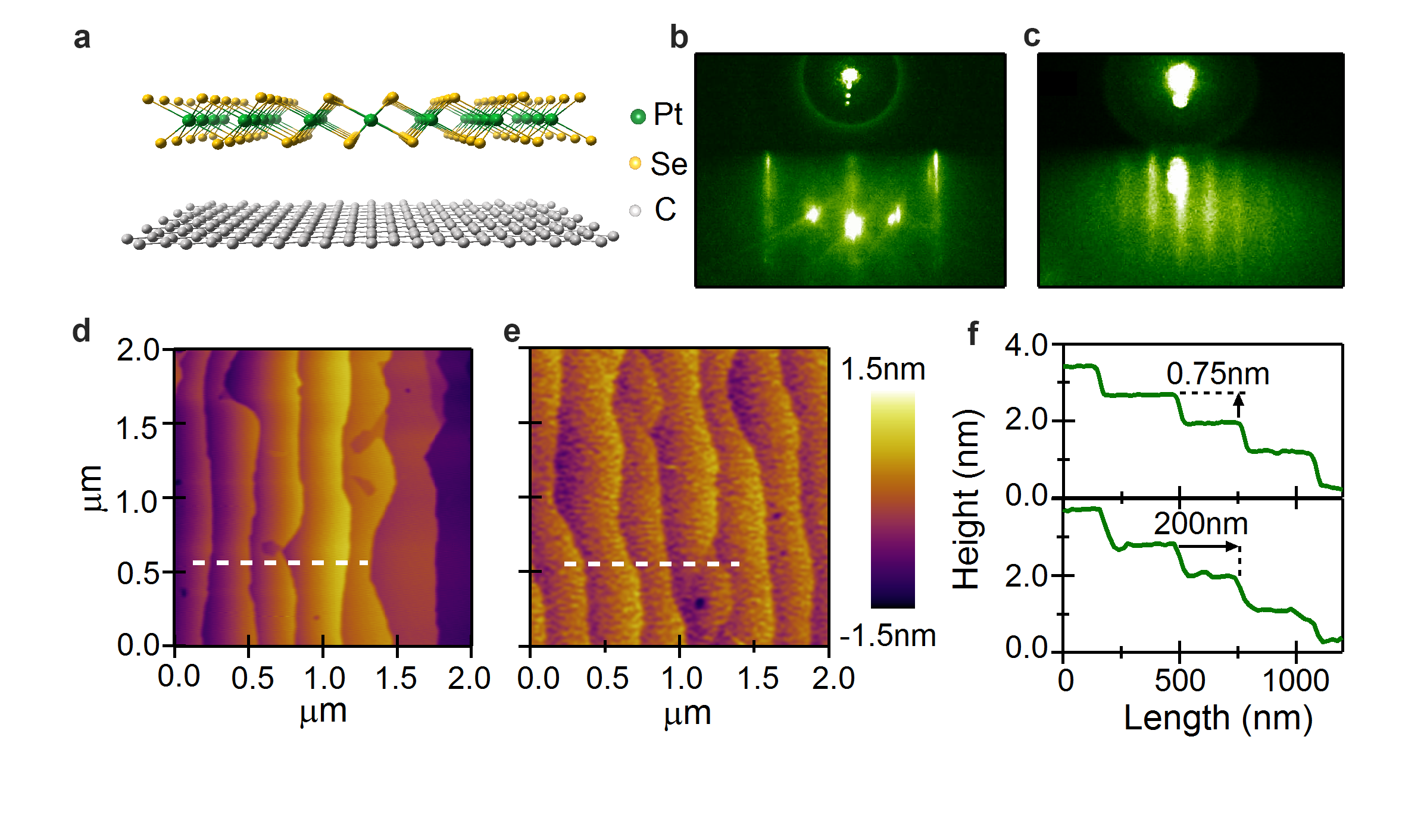
PtSe2 crystalizes in stable 1T phase corresponding to the CdI2-type trigonal structure with Pm1 space group (No. 162). The building block of PtSe2 contains one Pt atomic layer sandwiched between two Se layers, where Pt atoms are octahedrally coordinated by the Se atoms (Figure 1a). Atomically thin PtSe2 films with varying thickness from 1 ML to 22 ML were grown on bilayer graphene/6H-SiC (0001) substrates using a home built MBE system with a base pressure of 210-10 Torr. High-purity Se and Pt are evaporated to the substrate with a flux ratio of 15:1 with the substrate temperature held at 270 ∘C. The growth rate is controlled by the Pt flux and excess Se are desorbed from the substrate. The sample thickness is controlled by the growth time. Figure 1b,c show the RHEED patterns before and after growth of the PtSe2 film. RHEED spots from the substrate are completely covered by sharp streaky stripes from the film within the first minutes of growth. The surface morphology of the substrate is revealed by AFM image (Figure 1d), with an average terrace of 200 nm and a step height of 0.75 nm (Figure 1f) which is the typical height of triple SiC bilayer steps.27 The overall substrate steps are preserved after growth of the PtSe2 film (Figure 1e), indicating the uniform epitaxy growth along the graphene steps. Compared with samples prepared by CVD or TAC, our MBE films have significantly improved crystallinity, homogeneity and continuity in large scale as well as better thickness control at atomic level. Such high quality single crystalline films provide a unique opportunity for a systematic study of the evolution of the vibrational and electronic properties as a function of sample thickness.
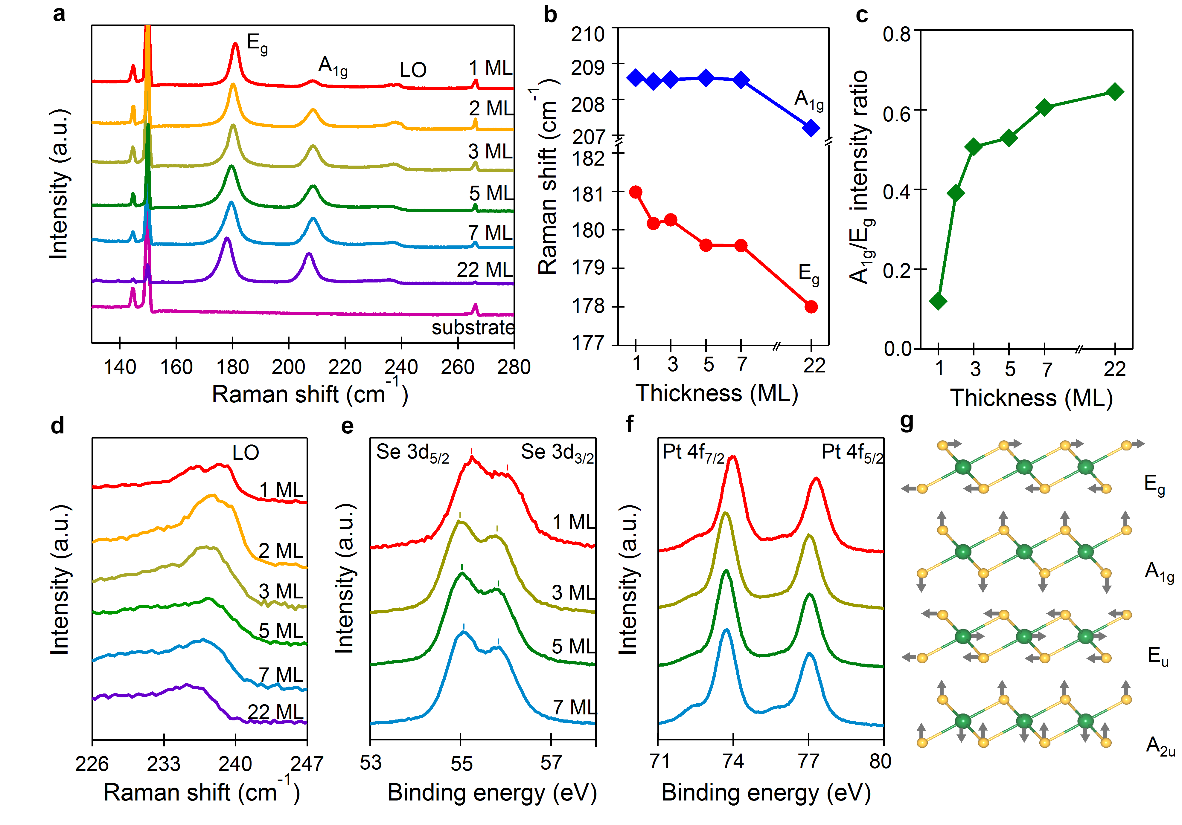
The MBE grown PtSe2 films are characterized by Raman spectroscopy and XPS. Figure 2a shows the Raman spectra of PtSe2 films with varying thicknesses. The high quality films result in sharper spectra than exfoliated flakes 14 and three peaks are clearly identified as Eg, A1g and LO. In all PtSe2 films, two prominent peaks at 180 cm-1 and 208.5 cm-1, correspond to the Eg and A1g Raman active modes respectively. 23, 24 The Eg mode corresponds to an intra-layer in-plane vibration of Se atoms moving in opposite directions and the A1g mode involves the out-of-plane vibration of Se atoms moving away from each other. The Eg mode shows a clear blue shift with decreasing film thickness (Figure 2b), while the A1g mode is pinned at 208.5 cm-1 at the first few layers thin film. A red shift of A1g peak is also observed in thicker (22 ML) PtSe2 film, which is less significant compared with Eg mode. This anomalous behavior may be attributed to stacking-induced structural changes and long-range Coulombic interlayer interactions. 28, 23 Moreover, the peak intensity of the A1g mode relative to that of the Eg mode is strongly pronounced from 1 ML to 22 ML (Figure 2c), consistent with the enhanced van der Waals interactions in thicker films. 28 The peak at 240 cm-1 is attributed to a longitudinal optical (LO) mode, which is a combination of the out-of-plane (A2u) and in-plane (Eu) vibrations of platinum and selenium atoms respectively, with a similiar origin to those observed in HfS2, ZrS2 and CdI2. 29, 30 The zoom-in spectra in Figure 2d show the strongest LO mode in 1 ML PtSe2 film that splits into two peaks at 236 cm-1 and 239 cm-1. With increasing thickness, such two peaks merge into a broader and weaker peak. Figure 2e-f shows the XPS spectra of Pt and Se. A blue shift of Se 3d and Pt 4f core levels by 240 meV (Figure S2 in the supplementary information) suggests the different chemical environment in 1 ML film. The shift of the core level to higher binding energies suggests that there is likely charge transfer between the substrate and the first PtSe2 layer.
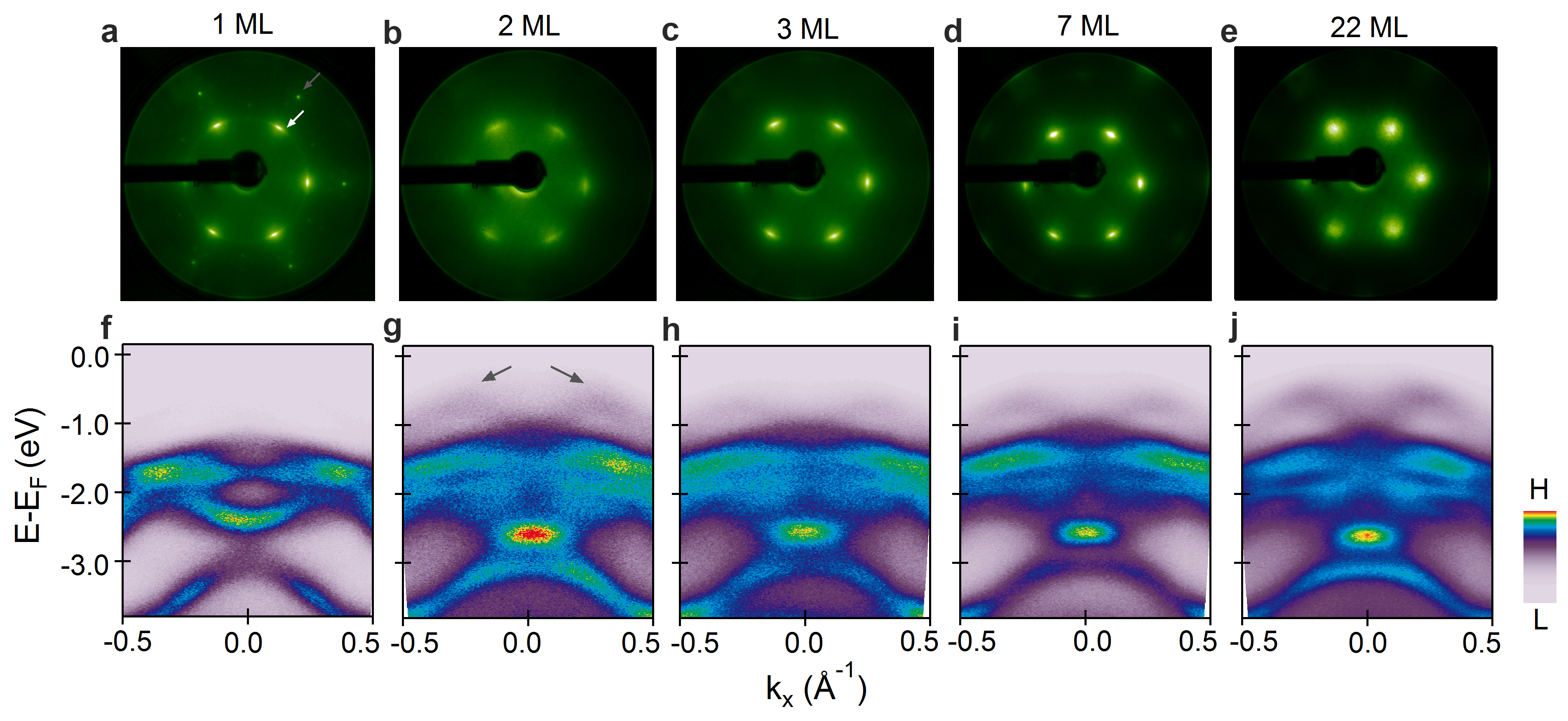
To reveal the evolution of the electronic structure as a function of film thickness, we show in Figure 3 LEED and ARPES data taken from 1 ML film to 22 ML PtSe2 films. Figure 3a-e shows LEED patterns with different film thickness. In 1 ML film (Figure 3a), both the signals from the PtSe2 film (indicated by white arrows) and the substrate (grey arrow) are observed. PtSe2 grows mainly along the orientation of the graphene substrate with some small azimuthal deviations due to the weak coupling between PtSe2 and graphene, showing an arc-like feature in LEED signal. As the growth proceeds (Figure 3b-e), the substrate is completely covered by PtSe2 and the LEED pattern from graphene disappears. ARPES dispersions measured along the -K high symmetry direction are shown in Figure 3f-j. Our data of 1 ML PtSe2 film (Figure 3f) matches well with previous work on 1 ML PtSe2 film grown by direct selenization method, 12 showing a semiconductor with the top of the valence bands at -1.2 eV. For films thicker than 1 ML, an additional band with an M-shape (indicated by gray arrow in Figure 3g) emerges. This band moves toward the Fermi energy, indicating a reduction of the band gap as predicted. 31 The M-shape valence band eventually develops into a three dimensional Dirac cone in the bulk topological Dirac semimetal. 10, 11 By increasing the film thickness, the 22 ML PtSe2 film shows effectively the same electronic band structure as the bulk Dirac semimetal except a 350 meV charge transfer from the substrate (Figure S3 in the supplementary information). The ARPES experiments thus provide a direct evidence for the tunable bandgap with varying film thickness.
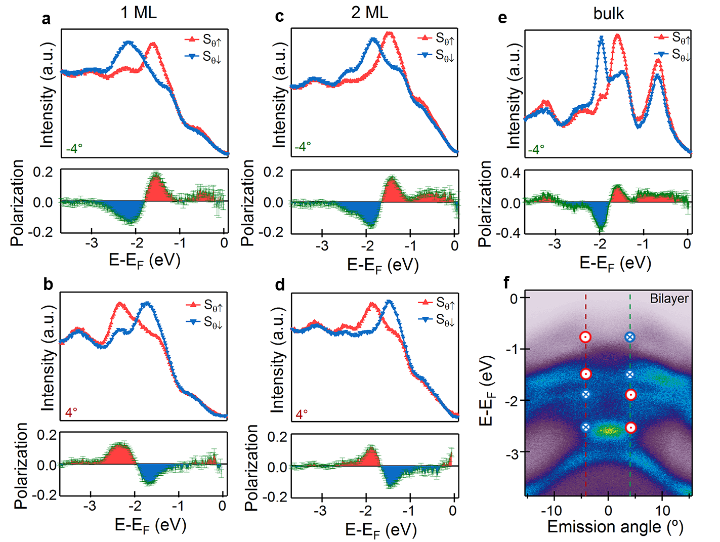
We further perform spin-ARPES measurements to reveal the spin texture of PtSe2 films. Figure 4a-d shows spin-ARPES measurements along the -K and -K′ high symmetry directions of both 1 ML and 2 ML films. Large spin contrast is observed along the tangential direction () at emission angles of and , respectively (dahsed line in Figure 4f). The radial (r) and out-of-plane () directions show negligible spin contrast (Figure S4 in the supplementary information). This is consistent with the helical spin texture as previously reported in 1 ML PtSe2 films on Pt(111) substrate, 15 confirming that it is an intrinsic effect of the PtSe2 film. Similar helical spin texture is also observed in centrosymmetric bulk PtSe2 crystals (Figure 4e), supporting the spin-layer locking mechanism induced by local Rashba effect 32. Such helical spin texture induced by local Rashba effect makes it useful for electric field tunable spintronics.
To summarize, we have successfully achieved layer-by-layer growth of high quality PtSe2 thin films with controlled thickness using MBE. The samples are characterized by Raman, XPS, LEED and the electronic structure is revealed by APRES. ARPES measurements reveal a distinct tunable bandgap in atomically thin films. The MBE growth can also be extended to insulating substrates. Combined with its unique high charge-carrier mobility and air stability, PtSe2 is a promising candidate for practical applications as new generation electronic devices. Our work reveals the interesting physics in thin PtSe2 films and the MBE growth can in principle be extended to grow large size single crystalline films on a variety of substrates.
This work is supported by the National Natural Science Foundation of China (Grant No. 11334006 and 11427903) and Ministry of Science and Technology of China (Grant No. 2015CB921001 and 2016YFA0301004).
1 METHODS
Thin film samples of PtSe2 were grown in an ultrahigh vacuum chamber with a base pressure of torr. The bilayer graphene substrates were prepared by flash annealing of the 6H-SiC(0001) to 1350 ∘C. The growth process was monitored by RHEED and the growth rate was 30 minutes per monolayer. During the growth process the substrate temperature was kept at 270 ∘C. After the growth, the sample was transferred to an ARPES chamber for measurements of the electronic band structure. ARPES measurements were taken with a Scienta R8000 electron analyzer using UV lamp (21.2 eV) at the temperature of 80 K in a vacuum higher than 110-10 Torr. XPS spectra of the Pt 4f and Se 3d core-levels were recorded under ultra-high-vacuum conditions better than 110-8 mbar on a VG Scientific ESCAlab MkII system using Al K X-rays and an analyzer pass energy of 30 eV. Raman spectra were measured on a Horiba Raman system with an excitation wavelength of 633 nm and a 1800 lines/mm grating. Spin-ARPES measurements were performed at ESPRESSO endstation of Hiroshima Synchrotron Radiation Center under the temperature of 20 K, using photon energies of 21.2 eV (UV lamp) and 21 eV (Synchrotron radiation).
References
- Wang et al. 2012 Wang, Q. H.; Kalantar-Zadeh, K.; Kis, A.; Coleman, J. N.; Strano, M. S. Nat. Nanotech. 2012, 7, 699–712
- Chhowalla et al. 2013 Chhowalla, M.; Shin, H. S.; Eda, G.; Li, L. J.; Loh, K. P.; Zhang, H. Nat. Chem. 2013, 5, 263–275
- Xu et al. 2014 Xu, X.; Yao, W.; Xiao, D.; Heinz, T. F. Nat. Phys. 2014, 10, 343–350
- Liu et al. 2015 Liu, G.-B.; Xiao, D.; Yao, Y.; Xu, X.; Yao, W. Chem. Soc. Rev. 2015, 44, 2643–2663
- Mak et al. 2014 Mak, K. F.; McGill, K. L.; Park, J.; McEuen, P. L. Science 2014, 344, 1489–1492
- Radisavljevic et al. 2011 Radisavljevic, B.; Radenovic, A.; Brivio, J.; Giacometti, V.; Kis, A. Nat. Nanotech. 2011, 6, 147–150
- Mak et al. 2010 Mak, K. F.; Lee, C.; Hone, J.; Shan, J.; Heinz, T. F. Phys. Rev. Lett. 2010, 105, 136805
- Yoon et al. 2011 Yoon, Y.; Ganapathi, K.; Salahuddin, S. Nano Lett. 2011, 11, 3768–3773
- Zhang et al. 2014 Zhang, W.; Huang, Z.; Zhang, W.; Li, Y. Nano Res. 2014, 7, 1731–1737
- Huang et al. 2016 Huang, H.; Zhou, S.; Duan, W. Phys. Rev. B 2016, 94, 121117
- Zhang et al. 2017 Zhang, K.; Yan, M.; Zhang, H.; Huang, H.; Arita, M.; Sun, Z.; Duan, W.; Wu, Y.; Zhou, S. arXiv preprint arXiv:1703.04242 2017,
- Wang et al. 2015 Wang, Y. et al. Nano Lett. 2015, 15, 4013–4018
- Qiao et al. 2014 Qiao, J.; Kong, X.; Hu, Z.-X.; Yang, F.; Ji, W. Nat. Commun. 2014, 5, 4475
- Zhao et al. 2017 Zhao, Y.; Qiao, J.; Yu, Z.; Yu, P.; Xu, K.; Lau, S. P.; Zhou, W.; Liu, Z.; Wang, X.; Ji, W.; Chai, Y. Adv. Mater. 2017, 29, 1604230
- Yao et al. 2017 Yao, W.; Wang, E.; Huang, H.; Deng, K.; Yan, M.; Zhang, K.; Okuda, T.; Li, L.; Wang, Y.; Gao, H.; Liu, C.; Duan, W.; Zhou, S. Nat. Commun. 2017, 8, 14216–14221
- Zhang et al. 2014 Zhang, X.; Liu, Q.; Luo, J.-W.; Freeman, A. J.; Zunger, A. Nat. Phys 2014, 10, 387–393
- Voiry et al. 2016 Voiry, D.; Yang, J.; Chhowalla, M. Adv. Mater. 2016, 28, 6197–6206
- Ye and Oh 2016 Ye, S.; Oh, W.-C. Mater. Sci. Semicond. Process. 2016, 48, 106–114
- Zhuang and Hennig 2013 Zhuang, H. L.; Hennig, R. G. J. Phys. Chem. C 2013, 117, 20440–20445
- Yu et al. 2016 Yu, X.; Peng, Y. U.; Liu, Z.; Wang, Q. CLEO: Science and Innovations 2016, STu4R.5
- Sajjad et al. 2017 Sajjad, M.; Montes, E.; Singh, N.; Schwingenschlgl, U. Adv. Mater. Interfaces 2017, 4, 1600911
- Wang et al. 2016 Wang, Z.; Li, Q.; Besenbacher, F.; Dong, M. Adv. Mater. 2016, 28, 10224–10229
- O’Brien et al. 2015 O’Brien, M.; Mcevoy, N.; Motta, C.; Zheng, J. Y.; Berner, N. C.; Kotakoski, J.; Elibol, K.; Pennycook, T. J.; Meyer, J. C.; Yim, C.; Abid, M.; Hallam, T.; Donegan, J. F.; Sanvito, S.; Duesberg, G. S. 2D Mater. 2015, 3, 021004
- Yim et al. 2016 Yim, C.; Lee, K.; McEvoy, N.; O’Brien, M.; Riazimehr, S.; Berner, N. C.; Cullen, C. P.; Kotakoski, J.; Meyer, J. C.; Lemme, M. C.; Duesberg, G. S. ACS Nano 2016, 10, 9550–9558
- Cho and Arthur 1975 Cho, A.; Arthur, J. Prog. Solid-State Chem. 1975, 10, 157–191
- Arthur 2002 Arthur, J. Surf. Sci. 2002, 500, 189–217
- Wang et al. 2013 Wang, Q.; Zhang, W.; Wang, L.; He, K.; Ma, X.; Xue, Q. J. Phys. Condens. Mater. 2013, 25, 095002
- Lee et al. 2010 Lee, C.; Yan, H.; Brus, L. E.; Heinz, T. F.; Hone, J.; Ryu, S. ACS Nano 2010, 4, 2695–2700
- Cingolani et al. 1984 Cingolani, A.; Ferrara, M.; Lugar, M.; Lvy, F. Solid State Commun. 1984, 50, 911–913
- Roubi and Carlone 1988 Roubi, L.; Carlone, C. Phys. Rev. B 1988, 37, 6808
- Huang et al. 2016 Huang, Z.; Zhang, W.; Zhang, W. arXiv preprint arXiv:1605.08536 2016,
- Zhang et al. 2014 Zhang, X.; Liu, Q.; Luo, J. W.; Freeman, A. J.; Zunger, A. Nat. Phys. 2014, 10, 387–393