Relativistic space-charge-limited current for massive Dirac fermions
Abstract
A theory of relativistic space-charge-limited current (SCLC) is formulated to determine the SCLC scaling, , for a finite bandgap Dirac material of length biased under a voltage . In a one-dimensional (1D) bulk geometry, our model allows (, ) to vary from (2,3) for the non-relativistic model in traditional solids to (3/2,2) for the ultra-relativistic model of massless Dirac fermions. For a two-dimensional (2D) thin-film geometry, we obtain that varies between 2 and 3/2, respectively, at the non-relativistic and ultra-relativistic limits. We further provide a rigorous proof based on a Green’s function approach that for uniform SCLC model described by carrier density-dependent mobility, the scaling relations of the 1D bulk model can be directly mapped into the case of 2D thin film for any contact geometries. Our simplified approach provides a convenient tool to obtain the 2D thin-film SCLC scaling relations without the need of explicitly solving the complicated 2D problems. Finally, this work clarifies the inconsistency in using the traditional SCLC models to explain the experimental measurement of 2D Dirac semiconductor. We conclude that the voltage-scaling is a distinct signature of massive Dirac fermions in Dirac semiconductor and is in agreement with experimental SCLC measurement in MoS2.
pacs:
77.22.Jp, 72.10.-d, 73.63.-b, 73.50.-hI Introduction
Space-charge-limited current (SCLC) gives the maximum current that can be transported across a solid of length with a biased voltage , limited by the electrostatic repulsion generated by the in-transit unscreened charge carriers that are in excess of the thermodynamically allowed population lampert . In a trap-free bulk crystal, SCLC exhibits a signature current-voltage (-) characteristics of known as the Mott-Gurney (MG) law MG , which is the solid-state counterpart of the SCLC in vacuum as given by the Child-Langumir (CL) law: in classical regime CL ; Zhu and in quantum regime Ang ; Lau . Including defect states or traps in solids, SCLC becomes trap-limited as described by the Mark-Helfrich (MH) law mark : , where , is temperature and is a parameter characterizing the exponential spread in energy of the traps. Due to the geometrical effect grinberg , the 1D SCLC value is enhanced as a result of finite emission area chandra and weakened Coulomb screening in high aspect-ratio nanowire talin . Furthermore, SCLC is an important tool to probe the trap characteristics in solids, and also for photocurrent measurement since the extraction efficiency of photogenerated carriers is fundamentally limited by SCLC SCLPC .
For organic semiconductors, field-dependent blom ; bozano ; campbell ; ng and density-dependent mobility SCLC models tanase ; pasveer are commonly employed to characterize the SCLC carried by the holes. Similarly, SCLC of electrons was found to be universally described by a trap model with Gaussian energy distribution in a large class of organic semiconductors nicolai ; nicolai2 . Recently it is demonstrated that the magnitude of electron SCLC can be significantly enhanced via the dilution of traps in conjugated polymer blends of only 10% of active semiconductor abbaszadeh , which opens up an exciting possibility of high-efficiency and low-cost organic light emitting diode. SCLC in the trap-limited regime was re-formulated zhang with inclusion of the interplay between dopants and traps, Poole-Frenkel effect frenkel and quantum mechanical tunneling, which has solved the long-standing problem rose ; lampert2 of the enormously sharp current rise at the trap-limited regime and demonstrated that an exponentially distributed trap is not necessarily required to explain the power-law sharp rises of SCLC in the trap-limited regime. Remarkably, the model successfully reproduced the anomalous noise-spectrum peak observed in carbone .
In spite of SCLC being a classic model first derived in 1940s, it remains an active topic for organic materials and nanowires as mentioned above. With the advances in fabricating novel 2D Dirac materials graphene ; TI ; mos2_lit , it is of the interests to revisit the SCLC model for these 2D Dirac materials. To our best knowledge, there is no theory or model to deal with the SCLC transport in Dirac materials. Recent experiments reported a typical - characteristic in the form of MH law for highly disordered materials like reduced graphene oxide jung ; jung2 . On the other hand, SCLC in crystalline monolayer MoS2 mos2 and hBN hbn was found to exhibit an unusual power law dependence of with , which was claimed to be originated from the different levels of traps in different samples by using the traditional MH law. This explanation is doubtful as the traditional MH law is only valid for for , which implies that the voltage scaling from the MH law must be theoretically and it can not be used to fit with the mesured scaling of . For , the traps are narrowly distributed in energy space and the SCLC essentially reduces to single-level shallow trapping with rose . Thus, the observation of can not be explained by the MH law or other SCLC models such as shallow trap rose , Gaussian disorder gdm , field-dependent blom and density-dependent tanase mobility.
For a Dirac material with finite bandgap, the electrons mimics relativistic massive Dirac fermions mos2_band ; hbn_band whereas the classical SCLC models are based on the conduction model of non-relativistic quasi-free electrons lampert . In this work, we proposed a model of relativistic SCLC of massive Dirac fermions, which can explain the peculiar scaling observed in recent experiments using Dirac materials and thus circumvents the un-justified assumption of used in the MH law in order to fit the experimental data. According to our model, the - characteristics of SCLC in a 1D bulk geometry will vary between the non-relativistic limit of to the ultra-relativistic limit of (this is different from the CL law - see below for explanation). We present a master equation which is in good agreement with the experimental data and can be used to characterize the transition between the Ohmic conduction and SCLC regime. By extending the bulk 1D model to a 2D thin film model, the scaling relation becomes with varying between 3/2 and 2, respectively, at the ultra-relativistic and non-relativistic limits. In doing so, we prove rigorously, using a Green’s function approachgrinberg , that the 1D bulk SCLC current-voltage scaling relation can be directly mapped to 2D thin-film SCLC. It is shown that for a general transport equation of where is a mobility that depends on carrier density, , and is the electric field, the 1D bulk SCLC and 2D thin-film SCLC are linked by a universal SCLC scaling relation (see Section III). Our analysis provides a convenient tool to deduce the 2D thin-film SCLC scaling relation via simple 1D SCLC model without the need of explicitly solving the complicated 2D SCLC model.
II Theory of relativistic space-charge-limited current
In this section, a relativistic SCLC model is developed using semiclassical Boltzmann transport equation (BTE). For simplicity, we first consider the SCLC by assuming a simple 1D Poisson equation, which allows semi-analytical scaling relations to be determined. In Section III, we shall show that the simple 1D SCLC scaling relation derived in this section can be directly mapped to the case of 2D SCLC with thin-film geometry.
II.1 Boltzmann transport equation for conventional semiconductor
The starting point of the trap-free SCLC theory, i.e. the Mott-Gurney’s law, is the semiclassical BTE which provides a basic equation of current density governing the transport of charge carriers. The diffusion component is usually not considered except in some cases of polymers due to their highly disordered nature. For a quasi-static system, the BTE in the linearized transport regime under relaxation-time approximation is
| (1) |
where is the electric field, is the crystal momentum, is the position vector, is the carrier velocity, f is the out-of-equilibrium distribution function, is the equilibrium Fermi-Dirac distribution function, and is a typical collision time scale. If the system is spatially homogeneous the diffusion component of the transport current, i.e. , can be omitted. By assuming a 3D isotropic parabolic energy dispersion, one arrives at the well-known drift-current density, , for semiconductors:
| (2) |
By connecting the drift-equation with the 1D Poisson equation via charge density , the Mott-Gurney current-voltage scaling of can be recovered.
For 2D gapped Dirac materials, Eq. (2) is no longer valid due to two reasons: (i) the dimensionality is reduced to 2D; and (ii) the energy dispersion follows a relativistic dispersion similar to that of the massive Dirac fermions. In the following, we shall formulate the drift-equation for Dirac semiconductor based on BTE approach and demonstrate that the SCLC mediated by relativistic quasiparticles follows a completely different current-voltage scaling relation.
II.2 Boltzmann transport equation for 2D Dirac semiconductor
For massive Dirac fermions, the energy dispersion is where is the Fermi velocity, is the crystal momentum and is the bandgap. The group velocity is . The density of states , is rewritten as where denotes the spin-valley degeneracy and is a Heaviside function. The electron density at low temperature can then be obtained from the two-dimensional (2D) density of states which gives and is the Fermi level. The general expression of the 2D linear current density is where is the Fermi-Dirac distribution function, is the scattering time and is the externally applied electric field. In the low temperature limit, the current density can be analytically solved to give . Eliminating via , we obtain
| (3) |
where is a bandgap-dependent characteristic charge density, and are re-expressed as functions of the transport direction, . The term in Eq. (3) represents a major difference between the relativistic massive Dirac fermions and that of the non-relativistic quasi-free electrons. As , it can be seen from the - relation that the electrons are non-relativistic at very large or . For vanishingly small or , the electrons approach ultra-relativsitic limit and become massless Dirac fermions.
By expressing Eq. (1) in the Drude form of , a density-dependent Dirac mobility is defined as where . Consequently, the relativistic SCLC of massive Dirac fermions belongs to the class of density-dependent mobility SCLC. However, is unique to the massive Dirac fermions.
II.3 Relativistic SCLC in bulk geometry
We assume that the SCLC is carried solely by electrons injected through an Ohmic contact. For simplicity, we employ the 1D Poisson equation where , is the electrostatic potential, and is the effective dielectric constant. Here, we first assume that the 3D carrier density, , is related to via with as an effective thickness (see modification later). By coupling Eq. (3) with the Poisson equation via , we obtain the governing equation of the relativistic SCLC for Dirac solid:
| (4) |
We first investigate the solutions of the 1D relativistic SCLC, i.e. Eq. (4), in two asymptotic limits: (i) non-relativistic SCLC regime (); and (ii) ultra-relativistic SCLC regime (), which allows Eq. (3) to be approximated, respectively, as
| (5a) | |||||
| (5b) | |||||
The MG scaling is readily recovered from the non-relativistic charge dynamics at large . As the electrons reside just slightly above the bandgap where the inequality holds true, we have where . It can be shown fn1 that the corresponding current density is in the non-relativistic Drude form, which recovers the MG scaling of .
In the opposite limit of , implies ultra-relativistic dynamics with a scaling of as shown in Eq. 3(b). Coincidentally, this has the same scaling to the CL law CL although the underlying physics is fundamentally different. For Dirac materials studied there, the ultra-relativistic SCLC is obtained from
| (6) |
while SCLC in vacuum (or CL law) is obtained from
| (7) |
A simple dimensional analysis ang2 immediately shows that and are both proportional to albeit their very different origins. Nonetheless, Eq. (6) originates from the dependence owing to the ultra-relativistic electron dynamics in Dirac solids while Eq. (7) originates from the dependence owing to the energy balance of a non-relativistic free electron accelerating in vacuum. This demonstrates the fundamentally different mechanism behind the scaling in the two cases.
The two limits: and are, respectively, the extreme limits of the ultra-relativsitic and non-relativistic SCLC, an intermediate regime of is expected in the case of massive Dirac fermions. This is in good agreement with the experimental observations of in monolayer MoS2 mos2 and in monolayer hBN hbn where the charge carriers are essentially massive Dirac fermions. The model proposed here suggests that the scaling is to the relativistic carriers without the unjustified or invalid assumption of introducing traps with , which is also inconsistent with the original formulation of the MH law and other trap-limited SCLC models as discussed above.
For convenience, we transform Eq. (4) into a dimensionless form of
| (8) |
where and . The normalized current and the dimensionless parameter are
| (9a) | ||||
| (9b) | ||||
For a given value of and boundary conditions: and , Eq. (8) is solved numerically at various . The corresponding space charge limited current (SCLC) is determined when the value of will cause the onset of , and the calculated SCLC is plotted as a function of in Fig. 1(a), which exhibits contrasting behaviour at and at . For [Fig. 1(b)] and [Fig. 1(c)], the numerical results can be fitted by and , respectively, where . The contrasting -dependence can be understood from the dependence of , which corresponds, respectively, to the ultra-relativistic SCLC at (or small ), and the non-relativistic SCLC at (or large ). By substituting Eq. (9) into the above mentioned fitting equations, and are recovered, thus confirming the analytical solutions given in Eq. (5).
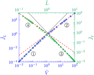
Figure 2 shows the smooth transition of and in between the ultra-relativisitc and non-relativistic regimes. The dimensionless current density - characteristic (at a fixed ) exhibits a voltage scaling of = 2 at low- and = 3/2 at high-. Here the dimensionless parameters are , , and . At a fixed , we have . and thus low- and high- correspond to the non-relativistic () and the ultra-relativistic () regimes, respectively as shown in Fig. 2 (blue axis, -symbols). In the intermediate regime, - deviates from the simple power law, and applying a fitting would lead to a sub-quadratic scaling in the range of .
Similarly, the dimensionless - characteristic (at a fixed ) shows a length scaling of of at small and at large , as shown in Fig. 2 (green axis, -symbols). Here, the dimensionless parameters are , , and . As , small and large corresponds to the non-relativistic and the ultra-relativistic regimes, respectively. The sub-cubic inverse length scaling represents another signature of the relativistic SCLC for Dirac solids in addition to the voltage scaling.
From Fig. 1(a), the numerical results over a wide range of can be accurately fitted by where . As all parameters are intrinsically contained in and , this empirical relation is universally valid and thus we derive a master equation that universally describes the SCLC transport over a wide range of parameters:
| (10) |
where is the total current, is the device width, and
| (11a) | ||||
| (11b) | ||||
It is important to emphasize that Eq. (10) is extremely usefully if it is used to fit with the experimental - measurement (in the form of as a function of ) to determine the values of and , which can be subsequently used to determine the collision time scale by using Eqs. (9) if the other parameters are known.
For the ultra-relativistic limit at , Eq. (10) becomes which confirms the ultra-relativistic scaling of . For the non-relativistic limit at , Eq. (10) reduces to which recovers the classical MG scaling of as expected. Therefore, the intermediate relativistic SCLC will produce a positive intercept on the vertical-axis of - characteristic whereas the SCLC with non-relativistic scaling will have a zero intercept as shown in Fig. 3(b).
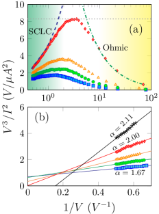
Interestingly, the - characteristic [suggested in Eq. (10)] provides a convenient tool to represent the SCLC data that can be generally applied to any solids. To illustrate this point, we consider a trap-free solid in which the conduction transits from Ohmic to SCLC at increasing as showin in Fig. 3a. In the Ohmic regime (large or small ) where , we have , i.e. decreases with increasing (green dash-dotted line in Fig. 3a). In contrast, in the SCLC regime (small or large ) where , we have , i.e. increases linearly with (blue dashed line in Fig 3a). These contrasting behaviors lead to a peak fn2 in the intermediate regime that clearly separates the SCLC-dominated and Ohmic-dominated conduction as shown in Fig. 3(a). This finding is confirmed by using various experimental data (color symbols) for MoS2 from Ref. mos2 at different temperature as shown in Fig. 3a. The above mentioned transitional peak between SCLC-dominated regime (dashed curve) and Ohmic-dominated regime (dash-dotted curve) can be clearly observed at all temperatures.
A zoom-in view at the small- SCLC-dominated regime is shown in Fig. 3(b), which indicates that the experimental results (symbols) can be explained by linear fitting so to obtain the voltage scaling, which ranges from = 2.11 down to 1.67 according to Eq. (10). The scaling decreases to at elevated temperature because the higher energy levels of the conduction band is increasingly populated by the thermally-liberated electrons from trapping sites. This leads to a higher-degree of relativistic dynamics of the transport electrons thus reducing . For the three cases, they can be extrapolated to have positive intercepts on the -axis at 0 [see Fig. 3(b)]. As approaches 2, the intercepts diminishes and becomes approximately zero at . These observations are in good agreement with the predicted intercepts of Eq. (10), as discussed above. Note that Eq. (10) breaks down in the case of where the intercept becomes negative.
III Simplified model of uniform SCLC injection in 2D Dirac semiconductor
The relativistic SCLC model derived above is based on solving the 1D Poisson equation. As Dirac semiconductor is a 2D thin film, thus a 2D thin-form model is required. In this Section, we provide a simplified formalism of 2D thin-film relativistic SCLC model without the need to explicitly solve for the 2D model grinberg .
III.1 Universal model of -dimensional uniform SCLC injection in solid with density-dependent mobility
The SCLC has been previously formulated for thin-film and nanowire using an integral form of 2D electrostatic Poisson equation grinberg ; talin . Here, we shall formulate a thin-film SCLC relativistic model under the assumption of carrier density-dependent mobility to illustrate that the general SCLC scaling properties for Dirac semiconductor, which has a density-dependent mobility of .
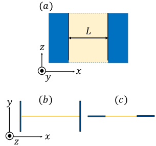
We consider the -dimension transport in a solid with density-dependent mobility in a general form of where is a density-dependent term and is a constant factor. The dimensionality of and corresponds to bulk and 2D thin film, respectively. In the following analysis, we consider the case of uniform SCLC injection where the two electrodes are separated by a fixed spacing of as shown in Fig. 4(a). For uniform SCLC injection along the -direction, the electric field profiles, i.e. for bulk () and thin film () can be written, respectively, as
| (12a) | ||||
| (12b) | ||||
where and denote the surface and volume carrier density respectively. and is, respectively, the 1D and 2D Green’s function that are dependent on the geometry of contacts. Figures 4(b) and (c) shows a 2D thin film with two possible contact geometries, i.e. edge and strip contacts, respectivelygrinberg . By eliminating the -integration via and suppressing the argument of in Eq. (12b) for simplicity, Eq. (12) can be written compactly as
| (13) |
where we have introduced dimensionless variable as , and the subscript of denotes surface and bulk carrier density, respectively. Consider the charge transport mechanism in Dirac solid belongs to the class of density-dependent mobility model, we assume a general current density of
| (14) |
where the subscript denotes linear and areal current density respectively. The density-dependent mobility is given as where is a -dependent term and is a normalization constant. From Eq. (14), the bias voltage relation: is written as
| (15) |
The solution of Eq. (15) gives the equation of SCLC. Its full solution require the knowledge of over the intervals from to , which can be obtained by solving the nonlinear integral equation in Eq. (13). Nonetheless, the scaling relations, i.e. - and -, can be readily deduced via a simple dimensional analysis grinberg without explicitly solving Eqs. (13) and (15).
To illustrate this, we first combine Eqs. (13) and (14) to obtain
| (16) |
From the Poisson equation, i.e. where is a -dimensional Dirac delta function, the physical dimension of can be obtained as , where denotes the fundamental dimension of length and denotes the unit of physical quantity . Correspondingly, the partial derivative, , in Eq. (16) can be non-dimensionalized as
| (17) |
where is a dimensionless Green’s function. We now rewrite Eqs. (15) and (16) as
| (18a) | |||
| (18b) | |||
where for simplicity. A direct inspection of Eq. (18a) shows that after the integral is fully converted into a dimensionless form, the - and - scaling relations can be unambiguously determined. In this case, becomes a dimensionless numeric factor that does not play any roles in the - and - scaling relations.
The non-dimensionalization of Eq. (18a) can be accomplished by appropriately regrouping the constant term in Eq. (18b), i.e. into each of the and terms in the right-hand side of Eq. (18b) such that dimensionless terms and can be defined, respectively, for and . In general, the regrouping of can be expressed in an arbitrary form of
| (19) |
where and are terms containing and and are terms containing . The roles of ’s and ’s are to pair up with and in Eq. (18b) such that the resulting terms are dimensionless.
In the following, we suppress the argument of ’s and ’s for simplicity. As the explicit form of determines the regrouping of , ’s and ’s are both -dependent. Furthermore, ’s are -independent and ’s are -dependent as is deliberately distributed only into ’s. We can now recast Eq. (18b) as
| (20) |
where all terms are dimensionless via the following grouping
| (21) |
With and now being dimensionless, Eq. (18a) can be rewritten as:
| (22) |
or more compactly as
| (23) |
where is a dimensionless numeric factor dependent on the and , i.e.
| (24) |
which can be explicitly solved from Eq. (18b) and it affects only the overall magnitude of SCLC without affecting its voltage and length scaling relations. Thus the - and - scaling relations are determined by
| (25) |
III.2 Derivation of 2D thin-film SCLC scaling relations
Equation (25) represents a universal SCLC scaling relations for uniform SCLC injection into either a (bulk) or (thin film) based solid of length with arbitrary density-dependent mobility . Several remarkable properties can be extracted from Eq. (25): (i) The - scaling, i.e. , is determined solely by the and is completely independent on the device geometry () and dimensionality (); (ii) the - scaling, on the other hand, is affected by both and ; (iii) For a fixed (= 1 for bulk or = 2 for thin film), the geometry of contacts affects only and hence both SCL - and - scaling are universal independent on contact.
From Eq. (19), we see the constant term carriers a length scale dependence of , and thus Eq. (19) will be independent of for (for a thin film setting) resulting in . In this 2D thin film limit, Eq. (23) gives the SCLC relation for a thin film:
| (26) |
Note that Eq. (26) includes that both - and - follow the same scaling relation.
Togther with property (i) and Eq. (26), it shows a powerful tool that can be used to directly map the scaling relation of a simple bulk SCLC model into 2D thin-film SCLC model. By virtual of Property (i), we conclude that the voltage scaling for thin-film (-) is identical to the bulk - scaling, thus the voltage scaling obtained in Sec. II are valid for thin film as well. For a thin film, Eq. (26) also dictates that the length (-) scaling relation is identical to the -.
To summarize this session, we provide a rigorous derivation of scaling laws (both voltage and length) for uniform SCL injection into a 2D thin film seeting. These properties allow the - and - scaling relations of a 2D thin-film to be fully determined from a simple 1D bulk SCLC model that have been shown in Sec. II. The full - and - scaling relations are thus obtained without the need of explicitly solving the complicated coupled equations in Eq (18). In Appendix A, two examples of 2D thin-film SCLC are analyzed using our simplified formalism developed here.
III.3 Derivation of SCLC scaling relations and full numerical solutions of Eq. (18) for 2D Dirac semiconductor with traps
The relativistic SCLC scaling relation of Dirac semiconductor in 2D thin-film geometry can be readily determined by using the simple derivation developed above. Since the 1D SCLC scaling relations takes the form of and respectively for the ultra-relativistic and non-relativistic regimes, for 2D thin film, our simple analysis yields
| (27) |
where = 2 and = 3/2 are for the non-relativistic and ultra-relativistic limit, respectively. In the intermediate regime, the scaling follows an approximate power-law form with varies continuously from akin to Fig. 2.
To verify Eq. (27), the relativistic SCLC in 2D thin-film geometry with inclusion of exponential traps is explicitly solved (the full derivation is presented in Appendix B). In the presence of exponential traps, the relativistic SCLC in a 2D thin-film Dirac semiconductor is
| (28a) | ||||
| (28b) | ||||
where , is the 2D carrier density, , with as the effective density of states at the conduction band-edge and as the trap density, and are dimensionless variables. In the ultra-relativistic and non-relativistic SCLC regimes, we obtain and , respectively. By setting (which corresponding to a trap-free case), we obtain (non-relativistic) and (ultra-relativistic), thus confirming the simple derivation in Eq. (27). This agreement demonstrates that the unconventional - scaling of is a universal signature of the relativistic charge carrier dynamics in both bulk and 2D thin-film geometries.
In comparison to prior works in Ref. mos2 , the variation of to with decreasing temperature was attributed to the transition from (valid) to (invalid). Our relativistic SCLC model with exponential traps presented here is however ever to take account for such temperature dependence without imposing the invalid condition.
To further confirm that the analytical relativistic SLCC scaling relation obtained above, the integral equation in Eq. (28a), which belongs to the class of nonlinear Cauchy singular integral equation ladopoulos is numerically solved for the trap-free case of . The numerical solved [from Eq. (28a)] is then integrated in Eq. (28b) to obtain the as a function of . For simplicity, Eq. (28) is solved in terms of a dimensionless variables, i.e. and [see Appendix C and Eqs. (C6) and (C7) for the definition of and ]. The numerical results (red circles) of ) as a function of is shown in Fig. 5 show good agreement with the derived scaling laws: (dotted lines) at small voltage of and at large voltage of of . Thus, the comparison confirms the two corresponding analytical scaling laws [see Eq. (27)] for space charge limited conduction in a 2D thin-film Dirac solid with finite bangap: and respectively for the non-relativistic and ultra-relativistic limits. More importantly, the unconventional relativistic SCLC scaling of is unambiguously confirmed for the 2D thin-film Dirac semiconductor and is in agreement with experiments hbn ; mos2 .
Finally, we discuss the screening effect on the relativistic SCLC in 2D Dirac materials. In 2D Dirac materials, the charge transport is sensitively influenced by the substrate screening and excess charge screening induced by gate-electrode in field-effect-transistor geometry. Despite these screening effects, SCLC was unambiguously observed in experiments as reported in Refs. [31] and [32]. These experimental observations suggest that the screening effect cannot entirely remove SCLC in 2D materials. In a previous theoretical work jena , it is demonstrated that the surrounding dielectric screening will affect the transport properties of 2D thin film by modifying the relaxation time and a significant mobility enhancement can be achieved via high-κ dielectric substrate with vanishingly thin membrane. This theoretical prediction was experimentally confirmed in monolayer MoS2 with high-κ substrateradisaljevic . In relevance to our SCLC model, we point out that as the substrate screening effect alters only the relaxation time which comes into the SCLC picture as a proportionality constant, it can be reasonably expected that only the magnitude of the SCLC will be altered while the new scaling laws reported here will remain unchanged. A microscopic theory of substrate screening can be formulated via first-principle calculation that takes into account the complex many-body interactions at the interface between 2D materials and the substratekharche . The complete microscopic quantum picture od dielectric screening is beyond the scope of this work.
IV Conclusion
In summary, we have proposed a theory of relativistic space charge limited conduction (SCLC) in Dirac solids with new scaling laws for both bulk and thin file model. For the one-dimensional (1D) bulk model, the scaling laws are with and . For 2D thin film model, we have for uniform SCLC injection with remaining the same as the case of 1D bulk model under the assumption of density dependent mobility. Both scaling laws have been verified with numerical calculations and have good agreements with experimental results. The important finding from this paper is the new voltage scaling of which is a signature of the massive Dirac fermions in the 2D Dirac materials, and cannot be explained by using the traditional SCLC models derived decades ago for traditional materials. The inconsistencies in using such traditional SCLC models with unjustified traps condition to fit the experimental measurement is questionable. Our results represent a new class of relativistic space-charge phenomena in Dirac solids, which may be used to model Dirac-based devices operating in space-charge-limited regime and may also be used as a tool to extract useful parameters by fitting the analytical equations with measurements. The relativistic SCLC model should generate unconventional SCL photocurrent response SCLPC in relativistic Dirac semiconductor such as MoS2. The widely-studied photoresponse of MoS2 mos2_ph can be readily used as an additional platform to verify the proposed relativistic SCLC model here.
Acknowledgements.
We thank Subhamoy Ghatak for providing us the experimental data of MoS2 and insightful discussions. We thank Chun Yun Kee, Kelvin J. A. Ooi and Shi-Jun Liang for helpful discussions. This work is supported by Singapore Ministry of Education T2 grant (T2MOE1401) and USA AFOAR AOARD Grant (FA2386-14-1-4020).Appendix A Two examples of 2D thin-film SCLC using the simplified formalism
In this Appendix, we illustrates the simple derivation of the 2D SCLC scaling relations developed in Sections III-A and III-B using two examples. In the first example, we consider a trivial case with , i.e. the mobility is independent of carrier density. For bulk model of , Eq. (18b) becomes
| (29) |
which can be fully non-dimensionalized by defining , , and . From Eq. (23), we obtained , which can be rearranged to give the well-knwon bulk MG law of
| (30) |
The numerical factor can be solved as via Eq. (24) by using a 1D Green’s function grinberg . We can now map the - bulk SCLC scaling relation to the 2D thin-film case, which yields . Furthermore, as - scales equally with -, the 2D thin film SCLC scaling relation can now be fully determined as . One can verify this scaling relation by explicitly solving Eq. (26) with and . This gives , which can be rearranged to give the well-known 2D thin-film SCLC grinberg , i.e.
| (31) |
where is a -dependent numeric factor.
In the second example, we consider a carrier density dependent mobility in a power-law form, i.e. and where and are some constants. This particular form of is equivalent to Mark-Helfrich’s exponential-trap model with . For this particular form of , Eq. (18b) can be fully non-dimensionalized by re-grouping the constant factor via the following definitions: , , and . The bulk SCLC can then be obtained from Eq. (23) as
| (32) |
which can be simplified as
| (33) |
and is in agreement with the Mark-Helfrich’s exponential trap model mark . To generalize the bulk SCLC to the case of 2D thin film, we again utilize the facts that: (i) - follows the same scaling as -; and (ii) - scales equally with - This gives , which is in agreement with the explicitly solution of Eq. (26), i.e.
| (34) |
Appendix B Derivation of 2D relativistic SCLC model
In this Appendix, we provide a full derivation of the Mark-Helfrich’s SCLC model and Dirac semiconductor in 2D thin-film geometry based on Grinburg’s formalism grinberg .
B.1 Mark-Helfrich’s trap model of SCLC in 2D thin-film geometry
In the presence of traps that follows an exponential energy distribution mark , the free and trapped carrier densities are related by where is the free carrier density, is the trapped carrier density, is the effective density of states at the conduction band edge, is the trap density and . Here, where is a characteristic temperature representing the exponential spread in energy of the traps. The charge density in a 2D thin-film is given as
| (35) |
where is a Dirac delta function and is the charge density induced on the annode by the total residing in the thin film. Note that represent the direction that is out-of-plane of the thin film. For thin-edge contacts, the corresponding Green’s function is
| (36) |
and the scalar potential can then be solved as
| (37) |
Simplify and knowing that , we obtain
| (38) |
By defining and , we obtained
| (39) |
We now consider a current density equation in Drude’s form, i.e.
| (40) |
By combining Eq. (B5) and (B6), we obtain
| (41) |
Equation (B7) can be rearranged as followed:
| (42) |
By defining
| (43) |
Eq. (B8) becomes
| (44) |
which is an integral equation that can be solved to obtain . The bias voltage can be obtained from and Eq. (B6) as
| (45) |
To obtain the exponential trap-limited SCLC in 2D thin film geometry with edge-contact, Eqs. (B9) and (B11) are combined to give
| (46) |
With the definition of , which is a constant that can be solved from the integral equation in Eq. (B10), we obtain
| (47) |
Equation (B13) gives the exponential trap-limited SCLC of a 2D thin film with edge-contact geometry [see Fig. 4(b)]. For strip-geometry [see Fig. 4(c)], the electric field is given as
| (48) |
where and . Using similar procedure, we obtain
| (49) |
which can be simplified to
| (50) |
From Eq. (B12), the SCLC current density equation is obtained as
| (51) |
where the numeric factor can be obtained by solving from Eq. (B16). In summary, the 2D thin-film uniform injection of SCLC in the presence of exponential traps follow the following scaling relation of
| (52) |
for both edge-and strip-contact geometries. More importantly, this scaling relation is in agreement with Eq. (A6) obtained using the simplified formalism.
B.2 Relativistic SCLC model for 2D massive Dirac fermions
For 2D Dirac semiconductor, we obtain
| (53) |
and
| (54) |
respectively for edge-contact and strip-contact. The applied bias voltage for edge-and strip-contact geometries become, respectively,
| (55) |
and
| (56) |
The coupled Eqs. (B19) to (B22) can be solved to obtain the relativistic SCLC in 2D thin-film geometry. Equations (B19) to (B22) has to be solved numerically. Nonetheless, in the non-relativistic and ultra-relativistic limits, semi-analytical scaling relations can be derived. We first consider the non-relativistic limit of for all with edge-contacts, Eqs. (B19) and (B21) can be approximated, respectively, by
| (57) |
and
| (58) |
By defining
| (59) |
we obtain
| (60) |
where is a numerical factor which can be solved from the nonlinear integral equation in Eq. (B19). By setting , the current-voltage scaling relation agrees with the 1D bulk model as shown in Eq. (5a) of the main text. The current-voltage scales equally with the current-length which is also in agreement with the simplified derivation of 2D thin-film SCLC scaling relation presented in Eq. (27) of the main text.
In the ultra-relativistic limit of , Eqs. (B19) and (B21) become, respectively,
| (61) |
and
| (62) |
where
| (63) |
which can be rearranged to give
| (64) |
The numerical factor, , can again be solved from Eq. (B19). For , the current-voltage scaling relation agrees with the ultra-relativistic results in Eq. (5b) of the main text. In the intermediate regime, the scaling relation can be approximated by
| (65) |
where and .
Appendix C Equations (B28) to (B32) in dimensionless form
Equations. (B28) to (B32) can be transformed into a dimensionless form for numerical solution in Fig. 5 of main text. For edge-contacts, we obtain
| (66) |
and
| (67) |
For strip-contacts, the dimensionless form give
| (68) |
and
| (69) |
The dimensionless parameters are defined as
| (70) |
| (71) |
and
| (72) |
where is current-and material-dependent parameter.
References
- (1) M. A. Lampert and P. Mark, Charge Injection in Solids (Academic Press, New York and London, 1970).
- (2) N. F. Mott and R. W. Gurney, Electronic Processes in Ionic Crystals (Oxford University Press, New York, 1940).
- (3) C. D. Child, Phys. Rev. 32, 492 (1911); I. Langmuir, ibid 21, 419 (1921).
- (4) Y. B. Zhu, P. Zhang, A. Valfells, L. K. Ang, and Y. Y. Lau, Phys. Rev. Lett. 110, 265007 (2013).
- (5) L. K. Ang, T. J. T. Kwan and Y. Y. Lau, Phys. Rev. Lett. 91, 28303 (2003).
- (6) Y.Y. Lau, D. Chernin, D. G. Colombant, and P.-T. Ho, Phys. Rev. Lett. 66, 1446 (1991).
- (7) P. Mark and W. Helfrich, J. Appl. Phys. 33, 205 (1961).
- (8) A. A. Grinberg, S. Luryi, M. R. Pinto and N. L. Schryer, IEEE Trans. Electron Dev. 36, 1162 (1989).
- (9) W. Chandra, L. K. Ang and K. L. Pey, Appl. Phys. Lett. 90, 153505 (2007).
- (10) A. A. Talin, F. Leonard, B. S. Swartzentruber, X. Wang and S. D. Hersee, Phys. Rev. Lett. 101, 076802 (2008).
- (11) A. M. Goodman and A. Rose, J. Appl. Phys. 42, 2823 (1972); V. D. Mihailetchi, J. Wildeman and P. W. M. Blom, Phys. Rev. Lett. 94, 126602 (2005).
- (12) P. W. M. Blom, M. J. M. de Jong and M. G. van Munster, Phys. Rev. B 55, R656 (1997).
- (13) L. Bozano, S. A. Carter, J. C. Scott, G. G. Malliaras and P. J. Brock, Appl. Phys. Lett. 74, 1132 (1999).
- (14) A. J. Campbell et al, Adv. Funct. Mater. 26, 3720 (2016).
- (15) T. N. Ng, W. R. Silveira and J. A. Marohn, Phys. Rev. Lett. 98, 066101 (2007).
- (16) C. Tanase, E. J. Meijer, P. W. M. Blom and D. M. de Leeuw, Phys. Rev. Lett. 91, 206601 (2003).
- (17) W. F. Pasveer et al, Phys. Rev. Lett. 94, 206601 (2005).
- (18) H. T. Nicolai, M. M. Mandoc and P. W. M. Blom, Phys. Rev. B 83, 195204 (2011).
- (19) H. T. Nicolai, M. Kuik, B. de Boer, C. Campbell, C. Risko, J. L. Bredas and P. W. M. Blom, Nature Mater. 11, 882 (2012).
- (20) D. Abbaszadeh et al, Nature Mater. 15, 628 (2016).
- (21) X.-G. Zhang and S. T. Pantelides, Phys. Rev. Lett. 108, 266602 (2012).
- (22) J. Frenkel, Phys. Rev. 4, 647 (1938); J. G. Simmons, ibid 155, 657 (1967).
- (23) A. Rose, Phys. Rev. 97, 1538 (1955).
- (24) M. A. Lampert, Phys. Rev. 103, 1648 (1956).
- (25) A. Carbone, B. K. Kotowska and D. Kotowski, Phys. Rev. Lett. 95, 236601 (2005).
- (26) A. K. Geim and K. S. Novoselov, Nature Mater. 6, 183 (2007).
- (27) M. Z. Hasan and C. L. Kane, Rev. Mod. Phys. 82, 3045 (2010); X. L. Qi and S.-C. Zhang, ibid 83, 1057 (2011).
- (28) K. F. Mak, C. Lee, J. Horne, J. Shan and T. F. Heinz, Phys. Rev. Lett. 105, 136805 (2010); B. Radisavljevic, A. Radenovic, J. Brivio, V. Giacometti and A. Kis, Nature Nanotech. 6, 147 (2011).
- (29) I. Jung, D. A. Dikin, R. D. Piner and R. S. Ruoff, Nano Lett. 8, 4283 (2008).
- (30) D. Joung, A. Chunder, L. Zhai and S. I. Khondaker, Appl. Phys. Lett. 97, 093105 (2010).
- (31) S. Ghatak and A. Ghosh, Appl. Phys. Lett. 103, 122103 (2013).
- (32) F. Mahvash, E. Parais, D. Drouin, T. Szkopek and M. Siaj, Nano Lett. 15, 2263 (2015).
- (33) H. Bassler, Phys. Stat. Sol. b 175, 15 (19; S. V. Novikov, D. H. Dunlap, V. M. Kenkre, P. E. Parris and A. V. Vannikov, Phys. Rev. Lett. 81, 4472 (1998).
- (34) G.-B. Liu, W.-Y. Shan, Y. Yao, W. Yao and D. Xiao, Phys. Rev. B 88, 085433 (2013); E. Cappelluti, R. Roldan, J. A. Silva-Guillen, P. Ordejon and F. Guinea, Phys. Rev. B 88, 075409 (2013); Q. H. Wang, K. Kalantar-Zadeh, A. Kis, H. N. Coleman and M. S. Strano, Nature Nanotech. 7, 699 (2012).
- (35) G. W. Semenoff, Phys. Rev. Lett. 53, 2449 (1984); R. M. Ribeiro and N. M. R. Peres Phys. Rev. B 83, 235312 (2011).
- (36) In this limit, the density of states is and the carrier density is . Correspondingly, the current density is and hence the SCLC reduces to the MG law, i.e. . Note that this is differ by a factor of 2 in comparison with Eq. (5). This is due to the different expansion scheme used in obtaining Eq. (5). The expansion of in Eq. (4) is performed after the -integration of the current density equation.
- (37) L. K. Ang, Y. Y. Lau and T. J. T. Kwan, IEEE Trans. Plasma Sci. 32, 410 (2004).
- (38) At the transitional regime where is approximately proportional to , becomes constant. This leads to the occurrence of a peak in the - plot.
- (39) E. G. Ladopoulos, Singular Integral Equations (Springer, New York, 2000)
- (40) D. Jena and A. Konar, Phys. Rev. Lett. 98, 136805 (2007).
- (41) B. Radisavljevic, A. Radenovic, J. Brivio, V. Giacometti and A. Kis, Nature Nanotech. 6, 147–150 (2011).
- (42) N. Kharche and V. Meunier, J. Phys. Chem. Lett. 7, 1526 (2016).
- (43) O. Lopez-Sanchez, D. Lembke, M. Kayci, A. Radenovic and A. Kis, Nature Nanotech. 8, 497 (2013); M. Buscema et al, Nano Lett. 14, 3347 (2014).