Effect of picosecond magnetic pulse on dynamics of electron’s subbands in semiconductor bilayer nanowire
Abstract
We report on possibility of charge current generation in nanowire made of two tunnel coupled one-dimensional electron waveguides by means of single magnetic pulse lasting up to 20 ps. Existence of interlayer tunnel coupling plays a crucial role in the effect described here as it allows for hybridization of the wave functions localized in different layers which can be dynamically modified by applying a time changeable in-plane magnetic field. Results of time-dependent DFT calculations performed for a bilayer nanowire confining many electrons show that the effect of such magnetic hybridization relies on tilting of electrons’ energy subbands, to the left or to the right, depending on a sign of time derivative of oscillating magnetic field due to the Faraday law. Consequently, the tilted subbands become a source of charge flow along the wire. Strength of such magneto-induced current oscillations may achieve even but it depends on duration of magnetic pulse as well as on charge density confined in nanowire which has to be unequally distributed between both transport layers to observe this effect.
pacs:
72.25.Dc,73.21.HbI Introduction
Single quantum wires (SQWr) are the objects in which the charge carriers are confined in two dimensions but can move freely (ballistically) along the wire on the distance exceeding .Fischer et al. (2006a) Due to quantized motion of electrons in transverse direction, their energies form continuous subbands, which are occupied up to the Fermi level and for this reason an activation of subsequent subband is visible as a sudden upward step in conductance measurements.Thomas et al. (1999); Smith et al. (2009) Thus SQWr may constitute a basic building blocks in vast majority of nanodevices designed for experiments probing the quantum phenomena in transport measurements.Yamamoto et al. (2012); Kumar et al. (2014); Hew et al. (2009); Bielejec et al. (2005)
If two SQWr are aligned laterallyEugster and del Alamo (1991); Yamamoto et al. (2012) or vertically,Fischer et al. (2006a); Fischer et al. (2005); Thomas et al. (1999) one over another, the electronic properties of such double quantum wire system (DQWr) are remarkably modified due to their electrostatic and tunnel coupling. For example, in vertically stacked DWQr system, the strength of tunnel coupling, besides the actual geometry of nanostructure, i.e. the width of a barrier separating the wires, can be selectively modified by applying external magnetic field.Thomas et al. (1999); Lyo (1996, 1999); Fischer et al. (2006a); Fischer et al. (2005); Chwiej (2016a, b) In particular the in-plane orientation of magnetic field plays a crucial role in transport measurements. Fischer et all. in workFischer et al. (2006a) by applying an in-plane magnetic field in longitudinal (along the wire) and then in lateral directions were able to identify single transport modes and the energy splittings between subsequent subbands. Generally, there are two kind of effects in which the magnetic field influences on a single electron’s wave function in DQWr. First, it squeezes it in each wire diminishing hence its tunneling motion which can be even completely turned off in strong fields giving two separated transport channels.Mourokh et al. (2007a) Second, it hybridizes the ground state and first excited state in vertical direction what modifies the energy subbands.Lyo (1996, 1999); Chwiej (2016a, b) Such hybridization is activated by the off-diagonal elements in Hamiltonian what transforms the subbands crossings in energy spectrum into avoiding crossings called pseudogaps.Lyo (1996); Chwiej (2016a) Occurrence of pseudogaps is visible as sudden drop in conductance for increasing Fermi energy what can be realized by applying appropriate voltages to the top and back gates.Smith et al. (2009); Bertoni et al. (2008) In recent years, attention of researchers mainly attract the many-body effects appearing in bilayer nanosystems which can be examined in quantum transport measurements. To name some, these studies focus on the formation of Wigner crystals,Galván-Moya et al. (2012); Yamamoto et al. (2012); Hew et al. (2009) properties of composite fermions in quantum Hall regime in bilayer systemsMueed et al. (2016), Coulomb drag currentsYamamoto et al. (2012); Reichhardt et al. (2011) or ferromagnetism which appearance in strictly one-dimensional systems is forbidden due to Lieb and Mattis theorem but as shown by Wang et all. in workWang et al. (2005) can potentially be realized in DWQR due to the inter-wire tunneling.
Quite recently Chwiej has introduced in work [Chwiej (2016c)] a simple model describing an interaction of single electron confined in vertical bilayer nanowire with a picosecond magnetic pulse.Auston (1975); Wang et al. (2008); Vicario et al. (2013) There was shown that the fast oscillating magnetic field can effectively change the motion energy of electron, provided that the magnetic field is perpendicular to direction of electron transport and to direction of interlayer tunnel coupling. In such case, electron can be magnetically accelerated in nanowire in a direction depending on polarization of magnetic stimulus and initial division of charge between the coupled layers.
Present work is an extension of that idea to a many-electron case. Here, electrons are confined in infinite nanowire that consists of two one-dimensional electron waveguides separated by thin tunnel barrier. We assume the wire operates in the ballistic regime and consequently the electrons are described by the Bloch statesIhnatsenka and Zozoulenko (2006) which form the subbands in energy spectrum . These subbands are sampled for discrete values of wave vector and the corresponding wave functions are involved in time-dependent DFT calculations. Calculated energies of chosen Bloch states allow to reconstruct the actual shapes of energy subbands when the considered nanosystem interacts with a single picosecond magnetic pulse. Results show that energy subbands can be tilted for short period of time due to interaction of electrons with oscillating magnetic field. That leads to imbalance between the number of electrons having positive and negative wave vectors in vicinity of the Fermi energy level. Such tilting of subbands directly generates a single charge current oscillation flowing along the wire. We show that amplitude of such magnetically induced current increases linearly with the duration of magnetic pulse. Moreover, we notice that the charge confined in nanostructure should be unequally distributed between two transport layers exactly as in a single electron problem.Chwiej (2016c) We indicate the last condition is crucial for considered effect to be observable.
The paper is organized as follows. In Sec.II we first describe in detail the structural properties of nanostructure we study, and then we present a DFT based numerical model used in calculations of energy spectra in nanowire. Section III is devoted to presentation and discussion of numerical results while conclusions are given in Sec.IV.
II Theoretical model
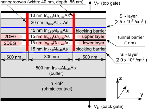
In the following considerations we assume the electrons are confined in vertical (z-axis) direction within two quantum wells made of which are separated by a thin barrier and are surrounded from bottom and top by wide barriers [see Fig.1]. The height of barriers equals . The electrons are provided by two donors layers localized below and above the double-quantum-well (DQW) structure. Due to proximity of these positively ionized doped layers ( below and above the DQW), the conduction band in DQW is bending toward the bottom and the top, in the lower and in the upper quantum wells, respectively.Fischer et al. (2006b); Chwiej (2016b) Such enhancement of vertical confinement within each quantum well leads to formation of two, the lower and upper, transport layers, which are tunnel coupled. The lateral confinement in y direction can be realized by application of anodic oxidization of surface technique. By ploughing the surface with an atomic force microscopy scanner, two parallel nanogrooves can be made,Levy et al. (2012); Apetrii et al. (2002) along x-axis in our case, which separate the electrons localized in the middle part of nanostructure from the left and right parts of the 2DEG [see Fig.1]. This central region forms actually the bilayer nanowire, in which the electrons can move freely along the wire but their motion in transverse directions becomes quantized. The electrons fill the DQW structure up to the Fermi energy level, which value is fixed at by two electron reservoirs (source and drain) attached to the ends of the lead. However both, the top gate covering the surface of nanostructure and the back gate lying at the bottom, allow changing the electron densities selectively in each layers by applying appropriate voltages to the top () and back () gates as has been shown in works by Fischer et al. [Fischer et al. (2006a, b)] for AlGaAs/GaAs heterojunction based nanostructure. Here we use similar geometry for nanostructure as the electrons confined in DQW have lighter effective mass ( versus ) what enhances their tunneling rate and speeds up the response of electron gas to the time variations of magnetic field.
Reaction of the conducting electrons to magnetic pulse and therefore the amplitude on magneto-induced current depends on the magnitude of hybridization in vertical parts of their wave functions.Lyo (1996); Fischer et al. (2006a); Chwiej (2016a) This, in turn, mainly depends on the interlayer tunnel strength and therefore of particular interest is determination of actual confining potential landscape. For this purpose we employ the electrostatic model described in work [Chwiej (2016b)] which has been worked out exactly for the geometry of nanodevice considered here.
We study the electronic structure of bilayer nanowire for Fermi energy exceeding and since single electron kinetic energy dominates over the electron-electron correlation energy,Yamamoto et al. (2012) we are justified in providing the further analysis of electronic properties in language of density functionals. Within DFT approximation Hamiltonian of single electron is given by
| (1) |
where is the conduction band effective mass in quantum well, is a momentum operator of electron, denotes an external confining potential, is an exchange-correlation potential calculated within a local-spin-density-approximation, while is the Coulomb part of electrostatic interaction obtained as solution of Poisson’s equation. The details of calculations of and are given in work [Chwiej (2016b)]. Second term in Eq.1 describes the contribution due to spin Zeeman effect with Lande factor , while the signs correspond to electron spin being parallel () and antiparallel () to magnetic field. For vector potential we use a non-symmetric gauge where and are defined as and with being a point at the center of tunnel barrier at half width of nanostructure shown in Fig.1. We assume , while changes with time. The following expression defines the time characteristic of magnetic pulse used in calculations
| (2) |
where is Heaviside step function, denotes the length of magnetic pulse and its frequency. For all results presented below the amplitude of magnetic pulse is . This value can be easily reached in practical realization with repetition frequency exceeding .Wang et al. (2008) Shape of magnetic pulse defined in Eq.2 is depicted in Fig.4(a). Due to the translational invariance of the confining potential, the wave function of electron with spin can be written as a plane wave
| (3) |
where describes the part of wave function for transverse direction,which generally can be time-dependent. In single particle picture involved here, the electrons have well defined wave vectors and form the energy subbands which are denoted by index . The main aim of this paper is to show the dynamic response of these subbands to stimulus in form of a picosecond magnetic pulse. By introducing the plane wave approximation in Eq.3 we assume that electrons move ballistically only along the wire, however they can still be scattered in vertical and lateral directions due to the combined effect of non-homogeneity in the confining potential and variations of which contributing to the magnetic force temporarily deflects the trajectories of electrons.[Chwiej (2016c)]
Calculations of are performed on a rectangular spatial mesh of nodes in y-z plane, that is, and for and . Including the Peierls phase shift in kinetic operator for mesh in x directionChwiej (2016b) () and then averaging the Hamiltonian (Eq.1) over the x variable, , one gets the effective energy operator for the wave function
| (4) | |||||
In Eq.4, is the sum of all potentials appearing in Hamiltonian (1) and the Zeeman term. The first kinetic term in Eq.4 depends on wave vector but also on and variables if the cyclotron frequencies and do not vanish.
From Eq.4 appears that although the variations of can not change the canonical wave vector , they may change both, the group velocity of electron (), assuming that , and its motion energy which contributes to total energy , since these two quantities are connected by formula
| (5) |
Let us note that the wave function must be dependent on the wave vector’s value if (and/or ) what influences on the group velocity of electron
| (6) | |||||
In such case, the effect of action of magnetic force on moving electrons relies on changing their localization in y direction in quantum wire what differentiates the confinement energies of carriers for different wave vectors. It means that all subbands have no longer simple parabolic shape.
To find out the dynamical subbands’ responses to magnetic pulse, the states are first prepared at , and then, their transverse parts evolve in time according to time-dependent Schrödinger equation . Initial wave functions are simply the eigenstates of Hamiltonian (4). They have been found during diagonalization of this energy operator on spatial mesh at central part of nanostructure shown in Fig.1 ( and ). The time evolution of subbands is performed with application of Magnus propagatorCastro et al. (2004) for discrete values of taken at with and , where is the Fermi wave vector for first subband while . In other words is the maximal wave vector of electrons in nanosystem, which should be determined separately for each initial state as it depends on voltages applied to the top and back gates as well as on strength of (other parameters of calculations such as dopants densities are fixed). In calculations we used the time step which guarantees stability of our numerical procedure and keeps errors on acceptable level. Every time steps, the spin densities () and total density () as well as the Hartree and exchange-correlation potentials are recalculated. The spin densities are determined as follows
| (7) | |||||
where n is the subband’s index, is Fermi-Dirac distribution function and is the energy of electron occupying subband with wave vector . In similar way we calculate the total charge current
| (8) |
Here the contribution to x-component of density current equals . Integrals in Eq.8 are computed numerically and the temperature of electron gas used in calculations is . In expression for the Fermi-Dirac distribution function is taken for . Thus, we explicitly assume that the backscattering resulting from intersubband scattering, which potentially may lead to momentum relaxation, is absent in our model because we work in the ballistic regime. However, an intersubband scattering without change of wave vector can still occur since it corresponds to mixing of two subbands by e.g. variations of what locally influences on energy subbands’ dispersionsChwiej (2016a, b) and according to formula (5) on group velocities.
III Results
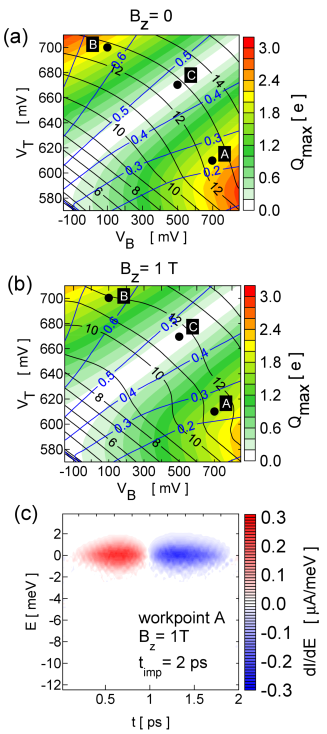
Figures 2(a) and 2(b) display the amplitudes of charge,
| (9) |
that flows through the nanowire when the electron gas confined in bilayer nanostructure interacts with magnetic pulse of duration. Let us note that changes qualitatively in the same way for and . Its value increases when division of charge density between the upper and lower layers is far from equilibrium (marked as white stripes). Then, the majority of electron density is localized in one layer what can be deduced from blue contours. Maxima of are localized in top-left and bottom-right corners of Figs. 2(a) and 2(b) showing thus strong dependence on gates biasing. This fact immediately implies that appropriate selection of and voltages shall enable one to choose the layer which holds the current and hence the direction of charge flow.[Chwiej (2016c)] Application of static vertical component of magnetic field () diminishes considerably. may completely disappear, provided that, the upper layer confines slightly less charge than the lower one what can be deduced from Figs. 2(a) and 2(b). In such case, the current is still induced, but it flows in opposite directions in upper and lower layers so both components cancel each other[Chwiej (2016c)] until separate gates are attached to the upper and to the lower layer as shown by Bielejec et al. in work [Bielejec et al. (2005)].
To get deeper insight into the dynamics of the electron subbands driven by time-varying magnetic field, the results for three arbitrarily chosen workpoints marked in Figs. 2(a) and 2(b) are analyzed in detail below. They are defined by pair of () voltages which are given in Tab.1.
| workpoint | |||||
| A | |||||
| B | |||||
| C |
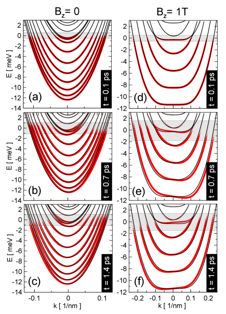
Fig.2(c) shows the energy resolved contributions to current in workpoint A with and . One can easily notice that the current is generated in vicinity of only indicating an imbalance introduced to subbands by . At first, when the polarization of magnetic pulse is positive, the current flows to the right and then it disappears when polarization is inverted. Afterwards the current starts flowing to the left. Due to symmetry of the magnetic pulse defined in Eq.2 the amount of charge that was initially shifted to the right and then to the left is almost identical. Corresponding energy subbands saved at three time instants for the workpoint A, , and are shown in Fig.3. At , when begins to grow, subbands (red dots) do not differ much from the initial ones (black lines) and the range of energy in which the Fermi-Dirac distribution function changes significantly is about [see the narrow horizontal grey strip in Figs. 3(a) and 3(d)]. At , the influence of magnetic pulse on subbands becomes noticeable, the branches with are lowered on energy scale while these with are lifted up widening hence the grey strip beyond an initial limit of . This remark, however, does not concern the , and subbands for . In these subbands the electrons occupy first excited state in vertical direction and therefore they are localized in different layer (the upper one) than these occupying the ground state in z (the lower layer). Such significant momentary tilt of subbands on energy scale has to generate the current flow in nanowire. According to Eq.8 contributions to currents from the left () and right () moving electrons do not cancel mutually on a short time scale introduced by magnetic pulse. Although, the energy shift between the states with and which belong to the same subband is larger for rather than for , the intensity of current and resulting value is larger in the latter case [compare the scales in Figs. 2(a) and 2(b)]. It results from the fact, that for there is active subbands near the Fermi level which contribute to total current in workpoint A whereas for there is only of them. One must keep in mind however, that for the slopes of subbands at Fermi level are noticeably larger than for what directly influences on current because of group velocity, given in Eq.5, what in turn partially diminishes the disproportion in current resulting from a large difference in number of active subbands. At polarization of magnetic pulse is reversed and for this reason subbands are tilted in opposite direction [cf. Figs. 3(c) and 3(f)] what obviously reverses the direction of current flow in nanowire [see Fig.2(c)].
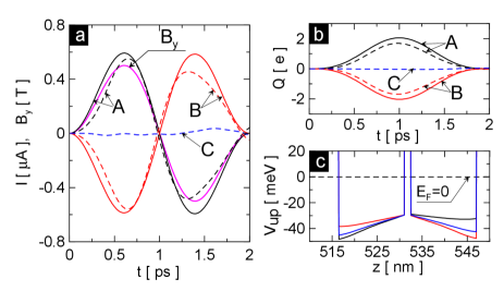
The time characteristics of current generated for workpoints A, B and C are shown in Fig.4(a). Even for short magnetic pulse () its amplitude reaches what makes its measurements experimentally feasible. One can notice in this figure, that the current pulses for workpoints A and B resemble very much the shape of the magnetic pulse [pink in Fig.4(a)] as they change their polarization exactly at . That means that the mass inertia of electron density does not influence on the dynamics of subbands. The time characteristics of current and charge flow [see in Fig.4(b)] can be to some extent modified by perpendicular magnetic field. For the amplitudes of both quantities have slightly lower amplitudes in comparison to results obtained for . Moreover they start growing with a certain delay what indicates on influence of magnetic forces. This issue will be analyzed in detail further in text. The momentary direction of current flow depends on whether the major part of charge density is localized in upper layer or in the lower one. Figure 4(c) shows the vertical profile of the confining potential in the center of nanowire. In workpoint A (black line) the majority of density is localized in the lower deeper layer, while in workpoint B the upper layer is deeper. For this reason, polarizations of current at these workpoints are opposite [see Fig.4(a)]. In third case, in workpoint C, both layers confine similar amount of charge, and hence the electrons confined in different layers are pushed in opposite directionsChwiej (2016c) giving thus no current flow [see Figs. 4(a) and 4(b)].
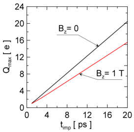
The amount of charge carried by single current oscillation depends on the length of magnetic pulse. As one may notice in Fig.5, dependence on is strictly linear but its slope decreases for . Thus, by tuning the values of parameters such as , , , one can carry, forward and backward, precisely determined amount of charge in bilayer nanowire.
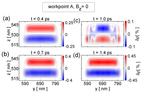
Now let us analyze the dynamics of intralayer and interlayer charge flow induced by magnetic pulse. Figure 6 shows the relative changes in spatial distribution of density in workpoint A for and . This quantity is defined as
| (10) |
where is the maximum of . At when the magnetic field is on its growing slope, a small part of density is carried from the deeper lower layer to the upper one. Note that the amount of density is evenly decreased in lower layer and evenly increased in the upper one. This process is continued until [compare scales in Figs. 6(a) and 6(b)] and afterwards an excess density comes back to lower layer what shows Fig.6(c) for . Next, although polarization of and generated current are reversed [see Fig.4(a)], part of the charge density flows again homogeneously from the lower layer to the upper one what is shown in Fig.6(d). The reasons of this homogeneous charge flow visible in Figs. 6(a), 6(b) and 6(d) are as follows. For , the dependence of on wave vector can be neglected and the whole energy subband can be described by single wave function. couples then both layers what hybridizes the ground state and the first excited state in vertical direction but simultaneously it leaves the lateral excitations (y direction) in unchanged. In other words, the wave function shape in this direction and the resulting lateral spatial distribution of charge density are preserved since both layers have comparable widths. This picture is valid only if the interlayer charge flow is large as it is shown in Figs. 6(a), 6(b) and 6(d). Then the contributions from the slowly oscillating in lateral direction lower subbands are significantly larger than these being provided by strongly oscillating subbands activated at higher energies what results from much larger imbalance between and branches in lowest energy subbands [see Figs. 3(b) and 3(c)]. If polarization of magnetic field is reversed what takes place at , contributions from all active subbands become comparable and as one may notice in Fig.6(c), oscillations in charge density occur near the edges of nanowire.
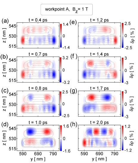
The mechanism of intralayer and interlayer charge redistribution driven by magnetic pulse is modified in presence of perpendicular magnetic field. In Fig.7, which shows for , we see that the interlayer charge flow is no longer homogeneous. First, the three lowest subbands for displayed in Figs.3(d)-(f) have flat bottoms and their energies strongly grow for large values what indicates formation of the edge states. Electrons obey then the Lorentz force which pushes electrons with and to the right and to the left edge, respectively.
When increases, from the Faraday’s law, , appears that the x-component of electric field induced in lower deeper layer accelerates the electrons with and decelerates these with . Electrons with are hence stronger pushed to the left edge what increases their energies, while the energies of electrons localized at the right edge () are decreased since these are pushed towards the center of quantum well [see energy subbands in Fig.3(e)]. As a result, a small fraction of charge is carried from the right edge to the left one in lower layer and simultaneously from the lower deeper layer to the upper shallower one for [Fig.7(a)]. Next, for the time interval the direction of induced electric field is reversed due to negative value of . For this reason, the excess charge localized in lower layer near its left edge is continuously carried to the right side, whereas the charge confined in upper layer flows in opposite direction but with some time delay [see Figs. 7(b)-7(f)]. This tendency holds until when induced electric field changes its direction again. That significantly diminishes the amplitude of charge oscillations in lower layer especially near the left and right edges [cf. Figs. 7(f) and 7(g)]. On the other hand it influences on charge oscillations in upper layer with some delay as these have larger amplitude at rather than those obtained for . Finally, when magnetic pulse vanishes for the amplitude of charge oscillations in both layers are reduced but they are still visible [Fig.7(h)]. Then, the charge distribution in lower layer resembles that obtained for because the directions of electric field induced in layers at the beginning and at end of the magnetic pulse are the same since . The density oscillations in upper layer are still distinct but they are two times frequent now what indicates the energy subbands lying higher on energy scale are more involved.
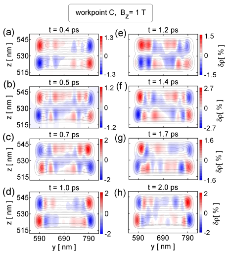
The time variations of in workpoint C for are presented in Fig.8. Since the upper and lower layers confine now and [see data in Tab.1] of charge, respectively, both layers play thus equivalent role in electron transport but their contributions to the current cancel each other. In other words, the magnetic pulse can not generate the charge flow between contacts attached to both ends of nanowire until these are independently connected with upper and lower layers as it was shown in work by Bielejec et al.Bielejec et al. (2005) However, it may induce local currents flowing in transverse directions. Snapshots of corresponding charge oscillations are displayed in Fig.8. Surprisingly, the effect of magnetic pulse on charge density in lower layer at is completely different than that observed in workpoint A [cf. Figs. 7(a) and Figs. 7(b)]. Namely, the electron density confined in lower layer is decreased at the left edge and increased on its right side [Fig.8(a)] while the pattern of charge oscillations in upper layer is inverted. Note, that for and , the rotational electric field induced by magnetic pulse accelerates the electrons localized in lower layer and decelerates these confined in upper layer, provided that considered electrons move near the left edge with . However, besides the change of electrons’ group velocities, magnetic pulse also bends their trajectories in vertical direction changing their tunneling motion. The magnitude of vertical component of magnetic force, besides the strength of magnetic pulse, depends also on the group velocity of electron. Therefore, the magnetic force enhances the charge flow towards the upper layer where the charge is accumulated but hinders the charge flow towards the lower layer where it becomes depleted. At the right edge, the direction of charge accumulation is reversed due to symmetry of the confining potential.
In workpoint C both layers have almost identical spatial sizes what implies that two subbands which are defined by the same excitation mode in lateral direction but differ in vertical excitation can be effectively hybridized by .Mourokh et al. (2007b); Fischer et al. (2006b) That is true, provided that is not strong, otherwise the lateral component of magnetic force may diminish hybridization since the wave functions’ maxima of involved subbands do not coincide. In workpoint C however, the charge can easily flow in vertical direction for independently on y-coordinate of an electron, whereas at workpoint A the charge flow from the lower layer to the upper one is blocked at edges by the potential barrier leading thus to its accumulation in lower layer. For this reason the maxima of visible in Fig.8 for () are localized in upper layer while for () in the lower one. Then, keeping in mind that the time derivative of has negative values only for , the distinct maximum appearing at the left edge in upper layer for longer time period, i.e. [see Fig.8(g)], unambiguously indicates on time delay in charge response to magnetic stimulus, likely due to a mass inertia of electron density.
IV Conclusions
In conclusion, the dynamics of energy subbands for electrons confined in bilayer nanowire was theoretically studied. It was shown that the time changeable magnetic field, which is perpendicular to the directions of electron transport and interlayer tunnel coupling, is able to change the shapes of energy subbands for a short period of time approaching . Due to the magnetic stimulus, the left and right parts of subbands can be raised as well as lowered on energy scale depending on the sign of and on division of total charge between two layers which has to be unequal. In such case, the momentary numbers of occupied states for and for become different what in turn induces the current flow along the wire. Shape and duration of such current pulse very well resemble that of magnetic stimulus, while its amplitude may reach , what makes its experimental confirmation feasible. Actual current intensity depends however on some factors such as the geometry of nanowire, density of dopants , strength and duration of magnetic pulse as well as on disproportion in amounts of charge confined in the lower and upper layers. The last factor can be easily modified by tuning the voltages applied to the top and back gates. We hope the results presented in this work will encourage experimentalists to perform measurements of magnetoinduced current for the nanodevice of the same or similar construction.
Acknowledgements
The work was financed by Polish Ministry of Science and Higher Education (MNiSW) and was supported in part by PLGrid Infrastructure.
References
References
- Fischer et al. (2006a) S. F. Fischer, G. Apetrii, U. Kunze, D. Schuh, and G. Abstreiter, Nat. Phys. 2, 91 (2006a).
- Thomas et al. (1999) K. J. Thomas, J. T. Nicholls, M. Y. Simmons, W. R. Tribe, A. G. Davies, and M. Pepper, Phys. Rev. B 59, 12252 (1999).
- Smith et al. (2009) L. W. Smith, W. K. Hew, K. J. Thomas, M. Pepper, I. Farrer, D. Anderson, G. A. C. Jones, and D. A. Ritchie, Phys. Rev. B 80, 041306 (2009).
- Yamamoto et al. (2012) M. Yamamoto, H. Takagi, M. Stopa, and S. Tarucha, Phys. Rev. B 85, 041308 (2012).
- Kumar et al. (2014) S. Kumar, K. J. Thomas, L. W. Smith, M. Pepper, G. L. Creeth, I. Farrer, D. Ritchie, G. Jones, and J. Griffiths, Phys. Rev. B 90, 201304 (2014).
- Hew et al. (2009) W. K. Hew, K. J. Thomas, M. Pepper, I. Farrer, D. Anderson, G. A. C. Jones, and D. A. Ritchie, Phys. Rev. Lett. 102, 056804 (2009).
- Bielejec et al. (2005) E. Bielejec, J. A. Seamons, J. L. Reno, and M. P. Lilly, App. Phys. Lett. 86, 083101 (2005).
- Eugster and del Alamo (1991) C. C. Eugster and J. A. del Alamo, Phys. Rev. Lett. 67, 3586 (1991).
- Fischer et al. (2005) S. F. Fischer, G. Apetrii, U. Kunze, D. Schuh, and G. Abstreiter, Phys. Rev. B 71, 195330 (2005).
- Lyo (1996) S. K. Lyo, J. Phys. Condens. Matter 8, L703 (1996).
- Lyo (1999) S. K. Lyo, Phys. Rev. B 60, 7732 (1999).
- Chwiej (2016a) T. Chwiej, Physica B 499, 76 (2016a).
- Chwiej (2016b) T. Chwiej, Physica E 77, 169 (2016b).
- Mourokh et al. (2007a) L. G. Mourokh, A. Y. Smirnov, and S. F. Fischer, Appl. Phys. Lett. 90, 132108 (2007a).
- Bertoni et al. (2008) A. Bertoni, S. F. Fischer, and U. Kunze, Physica E 40, 1855 (2008).
- Galván-Moya et al. (2012) J. E. Galván-Moya, K. Nelissen, and F. M. Peeters, Phys. Rev. B 86, 184102 (2012).
- Mueed et al. (2016) M. A. Mueed, D. Kamburov, L. N. Pfeiffer, K. W. West, K. W. Baldwin, and M. Shayegan, Phys. Rev. Lett. 117, 246801 (2016).
- Reichhardt et al. (2011) C. Reichhardt, C. Bairnsfather, and C. J. Olson Reichhardt, Phys. Rev. E 83, 061404 (2011).
- Wang et al. (2005) D.-W. Wang, E. G. Mishchenko, and E. Demler, Phys. Rev. Lett. 95, 086802 (2005).
- Chwiej (2016c) T. Chwiej, Phys. Rev. B 93, 235405 (2016c).
- Auston (1975) D. H. Auston, Appl. Phys. Lett. 26, 101 (1975).
- Wang et al. (2008) Z. Wang, M. Pietz, J. Walowski, A. Förster, M. I. Lepsa, and M. Münzenberg, J. Appl. Phys. 103, 123905 (2008).
- Vicario et al. (2013) C. Vicario, C. Ruchert, F. Ardana-Lamas, P. M. Derlet, B. Tudu, L. J., and C. P. Hauri, Nat. Photon. 7, 720 (2013).
- Ihnatsenka and Zozoulenko (2006) S. Ihnatsenka and I. V. Zozoulenko, Phys. Rev. B 73, 075331 (2006).
- Fischer et al. (2006b) S. F. Fischer, G. Apetrii, U. Kunze, D. Schuh, and G. Abstreiter, Phys. Rev. B 74, 115324 (2006b).
- Levy et al. (2012) E. Levy, I. Sternfeld, M. Eshkol, M. Karpovski, B. Dwir, A. Rudra, E. Kapon, Y. Oreg, and A. Palevski, Phys. Rev. B 85, 045315 (2012).
- Apetrii et al. (2002) G. Apetrii, S. F. Fischer, U. Kunze, D. Reuter, and A. D. Wieck, Semiconductor Science and Technology 17, 735 (2002).
- Castro et al. (2004) A. Castro, M. A. L. Marques, and A. Rubio, J. Chem. Phys. 121 (2004).
- Mourokh et al. (2007b) L. G. Mourokh, A. Y. Smirnov, and S. F. Fischer, Applied Physics Letters 90, 132108 (2007b).