Selective high frequency mechanical actuation driven by the \ceVO2 electronic instability
Abstract
This is the pre-peer reviewed version of the following article: “N. Manca et al. Adv. Mater. 29 (4), 1701618 (2017)”, which has been published in final form at: http://doi.wiley.com/10.1002/adma.201701618. This article may be used for non-commercial purposes in accordance with Wiley Terms and Conditions for Self-Archiving.
Ultra-thin free-standing structures such as membranes or microbridges can efficiently couple their mechanical degrees of freedom to electronic, optical and magnetic interactions in different excitation/response schemes Bunch et al. (2007); Van Thourhout and Roels (2010); Riedinger et al. (2016); Castellanos-Gomez et al. (2015). The use of materials with intrinsic functionalities and complex response to external stimuli constitutes the keystone towards next-generation miniaturized sensors and actuators Masmanidis et al. (2007); Park et al. (2011); Grover et al. (2011); Tao et al. (2014). To this purpose, transition metal oxides are a unique class of materials, where the balance between electronic correlations, magnetic ordering and lattice distortions gives rise to phase transitions and non-linear behaviours Imada et al. (1998); Morosan et al. (2012). Among them, \ceVO2 is considered a textbook example due to its metal-insulator transition associated with a crystal symmetry change when its temperature is increased above 65 ∘C Morin (1959). The phase transition of \ceVO2 is at the same time a puzzling mix of Mott physics, structural distortions Eyert (2002); Budai et al. (2014); Brockman et al. (2014); Kumar et al. (2014) and a unique candidate for a variety of technological applications Driscoll et al. (2009); Kats et al. (2013); Pellegrino et al. (2012); Shukla et al. (2015); Xiao et al. (2015); Yoon et al. (2016). One of the most fascinating characteristics of \ceVO2 is the possibility of realizing a current/voltage periodic instability under constant electrical bias that determines electrical oscillations. Spontaneous oscillations are a hallmark of non-linear systems Jenkins (2013), and in \ceVO2 they are triggered by the strong non-linear variation of its electrical properties across the phase transition. This oscillating state has been investigated in \ceVO2 bulk crystals Taketa et al. (1975); Fisher (1978) and more recently in single-crystal nano-beams and thin films Gu et al. (2007); Lee et al. (2008). Several studies showed how it is possible to control the frequency and the onset of this oscillating state by external parameters, such as device geometry, electrical bias, laser heating or by connecting electrical passive elements Kim et al. (2010); Seo et al. (2011); Kim et al. (2012); Wang et al. (2015). So far all these studies focused on the analysis of the electrical characteristics of this oscillating state, considering it a potential platform for neural-mimicking computing architectures Datta et al. (2014); Shukla et al. (2014); Beaumont et al. (2014); Pergament et al. (2016). However, since the phase transition of \ceVO2 involves both its electronic and lattice properties, electrical oscillations shall also determine a strong periodic mechanical forces on the device structure, whose implications have not been studied so far.
Here, we demonstrate how the coupled resistive and structural transition of \ceVO2 can be employed to generate mechanical excitations in the MHz range using only a DC voltage source. This is a local self-actuation mechanism capable of driving the motion of a micro-mechanical resonator, performing a direct transduction from a voltage bias to high-frequency mechanical excitation which relies on the intrinsic properties of \ceVO2 only. In contrast to the typical approaches of mechanical actuation Feng et al. (2008); Unterreithmeier et al. (2009); Baek et al. (2011), our scheme is intrinsic to the device and does not require dedicated driving electronics, reducing device complexity, size and power consumption.
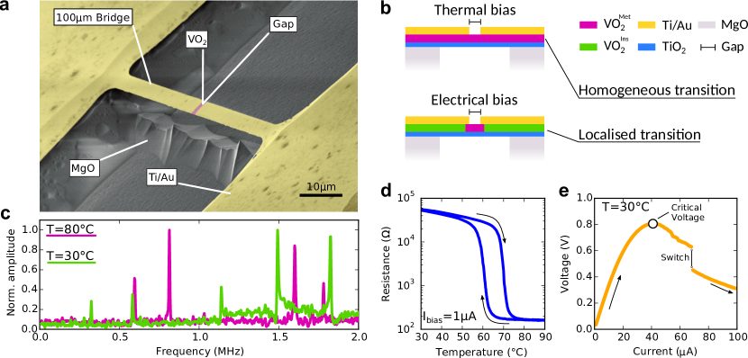
Our device is a free-standing microbridge made of a 113 nm-thick \ceTiO2 / VO2 crystalline bilayer. Metallic \ceTi / Au electrodes (50 nm-thick) partially cover the structure and provide good electrical contact (Fig. 1a). The \ceTiO2 / VO2 heterostructure is deposited by Pulsed Laser Deposition as described in the Methods. The resulting lattice is c-oriented with domains having orthogonal in-plane orientations Pellegrino et al. (2012); Okimura and Furumi (2005); Muraoka and Hiroi (2002). Details of the fabrication process can be found in the Methods section and in Supplementary section I, while further aspects of the device are discussed in the Supplementary section II. The phase transition (PT) of \ceVO2 is triggered above 64 ∘C, where its electrical resistivity drops by more than two orders of magnitude (insulator-metal transition) and the lattice symmetry changes from monoclinic to rutile (structural transition). Both effects are observed in the microbridge when it is homogeneously heated by an external thermal bias (Fig. 1b, top): the full bridge undergoes the PT, the lattice transformation causes a frequency shift of the mechanical modes up to 50 % (Fig. 1c and Supplementary section III) and the electrical resistance shows its characteristic hysteresis loops (Fig.1d). This frequency shift is due to the different in-plane lattice constants of \ceVO2 between the monoclinic and rutile phases Eyert (2002), that results in an isotropic strain of 0.08 % in the planar directions (See Supplementary section IV). As a consequence, the device experiences the stress-stiffening Karabalin et al. (2012) and geometric-stiffening Pini et al. (2016) effects, where the first is related to an increase of the tension within the structure and the second is a geometric deformation which both increase the structure rigidity. This wide variation of the internal mechanical stress across the phase transition has been recently exploited to realize tunable MEMS, like programmable resonators and static actuators Rua et al. (2010); Wang et al. (2013a); Manca et al. (2013); Liu et al. (2014); Merced et al. (2015); Ma et al. (2017). We note that the mechanical spectra of the microresonator, reported in Fig. 1c, differ from that of the simple double-clamped beam model. This because, as discussed in Supplementary section II, the device profile has a slightly buckled shape due to the built-in compressive stress within the heterostructure. In Supplementary section V we show finite elements simulations of the mechanical modes of our microbridge under buckling conditions and how strain can determine the measured frequency shifts.
In order to excite the resonator without altering its mechanical spectrum, we designed \ceTi / Au electrodes on top of the free-standing structure that leave a small active \ceVO2 region just within their gap, as indicated in Fig. 1a. Since the electrical and thermal resistivity of gold are negligible compared to \ceVO2, these electrodes localize the voltage drop on the \ceVO2 gap only and enhance its thermal contact with the clamped region. An electrical bias applied to the microbridge thus results in heating by Joule effect which is localized in the \ceVO2 gap, eventually triggering its PT. Here, the metal electrodes play the crucial role of limiting the spread of the \ceVO2 metallic phase (Fig. 1b, bottom), making the mechanical spectrum independent from the electrical current (See Supplementary section III). The voltage-current relationship of the microbridge is plotted in Fig. 1e, showing how the characteristic features given by \ceVO2 are retained. The non-monotonic behaviour with a negative differential resistance observed above 40 A and the sharp jump at 60 A are the key elements for the realization of electrical oscillations, as will be discussed below.
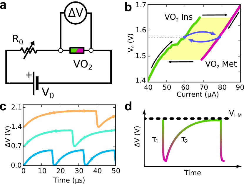
A consequence of the non-linear of \ceVO2 is the onset of electrical oscillations under DC bias. This state has been obtained using the circuit of Fig. 2a, where a DC voltage source () is applied to the \ceVO2 microbridge and a load resistor (). Their total voltage-current characteristic is reported in Fig. 2b and illustrates the origin of the electrical oscillations in the circuit. By sweeping the current magnitude, it is possible to track the hysteresis in the relationship due to the PT in the \ceVO2. At around 70 A the \ceVO2 switches from insulating (green) to metallic (magenta) state, with lower electrical resistance. When the circuit of Fig. 2a is biased with a DC voltage, the hysteresis window determines a range of values where two current conditions are allowed (yellow region). Under a constant voltage bias (dashed line), the voltage drop across the microbridge depends on the metallic or insulating state of \ceVO2. In the insulating state the voltage is localized across the microbridge by choosing the values of well below the electrical resistance of the \ceVO2 element. The resulting temperature increase can trigger the PT, lowering the microbridge electrical resistance. In this case the voltage drop is mainly across the load resistor and the Joule heating on the microbridge is reduced, the temperature decreases and the initial insulating state is recovered starting a new cycle. This continuous switching is a relaxation-oscillation condition Jenkins (2013), and is triggered for specific combinations of and Maffezzoni et al. (2015). Fig. 2c shows the voltage drop across the microbridge as a function of time while the electrical oscillations are triggered for and different between 10 k and 20 k. These electrical oscillations have a double-exponential wave-shape (Fig. 2d), where the time constants and of the semi-periods are determined by the thermal and electrical RC constants of the system. Their amplitude is constant and is determined by the critical voltage for the insulator-to-metal transitions of the \ceVO2 element ( of Fig. 2d). The electrical oscillation frequency (), instead, can be controlled from 20 kHz to 150 kHz by adjusting and .
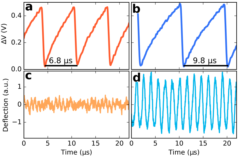
By tuning it is possible to excite the mechanical motion of the microbridge. This is detected by measuring the deflection of the device with an optical lever setup, while the DC circuit is set to trigger the electrical oscillations (see Supplementary section VI). Fig. 3 shows the time plots of the voltage drop measured across the microbridge (a, b)and its corresponding mechanical deflection (c, d) while the electrical oscillations are present. For a generic combination of and , the mechanical motion has small amplitude and no dominant harmonic component (a, c). However, for specific values of these parameters, and consequently specific , a strong harmonic mechanical response is observed at frequencies much higher than the electrical one (b, d). This response corresponds to a mechanical resonance of the microbridge as measured in Fig. 1c, meaning that, for specific values, the low-frequency electrical oscillations trigger resonant motion of the microbridge well above . As discussed in the next section, this is possible because the relaxation oscillation is non-sinusoidal and thus containing higher frequencies harmonic components.
The coupled electronic and structural transition of \ceVO2 make possible three parallel mechanisms to achieve mechanical actuation: actuation by structural transition, actuation by thermal expansion and electrostatic coupling. The first mechanism comes from the \ceVO2 lattice change during the PT, where the unit cell periodically expands and contracts when switching between the insulating/monoclinic and metallic/rutile phases. Thermal excitation comes from the Joule heating produced by the oscillating current, which results in a periodic thermal expansion of the structure. The electrostatic actuation originates from the periodic oscillation of the microbridge voltage with respect to ground which produces a net capacitive force coupled to the surrounding dielectric environment. All these three components are periodically modulated by the \ceVO2 PT and can contribute synergistically to the mechanical actuation with a periodic excitation at and its higher harmonics. An evaluation of their magnitude is presented in Supplementary section VII.
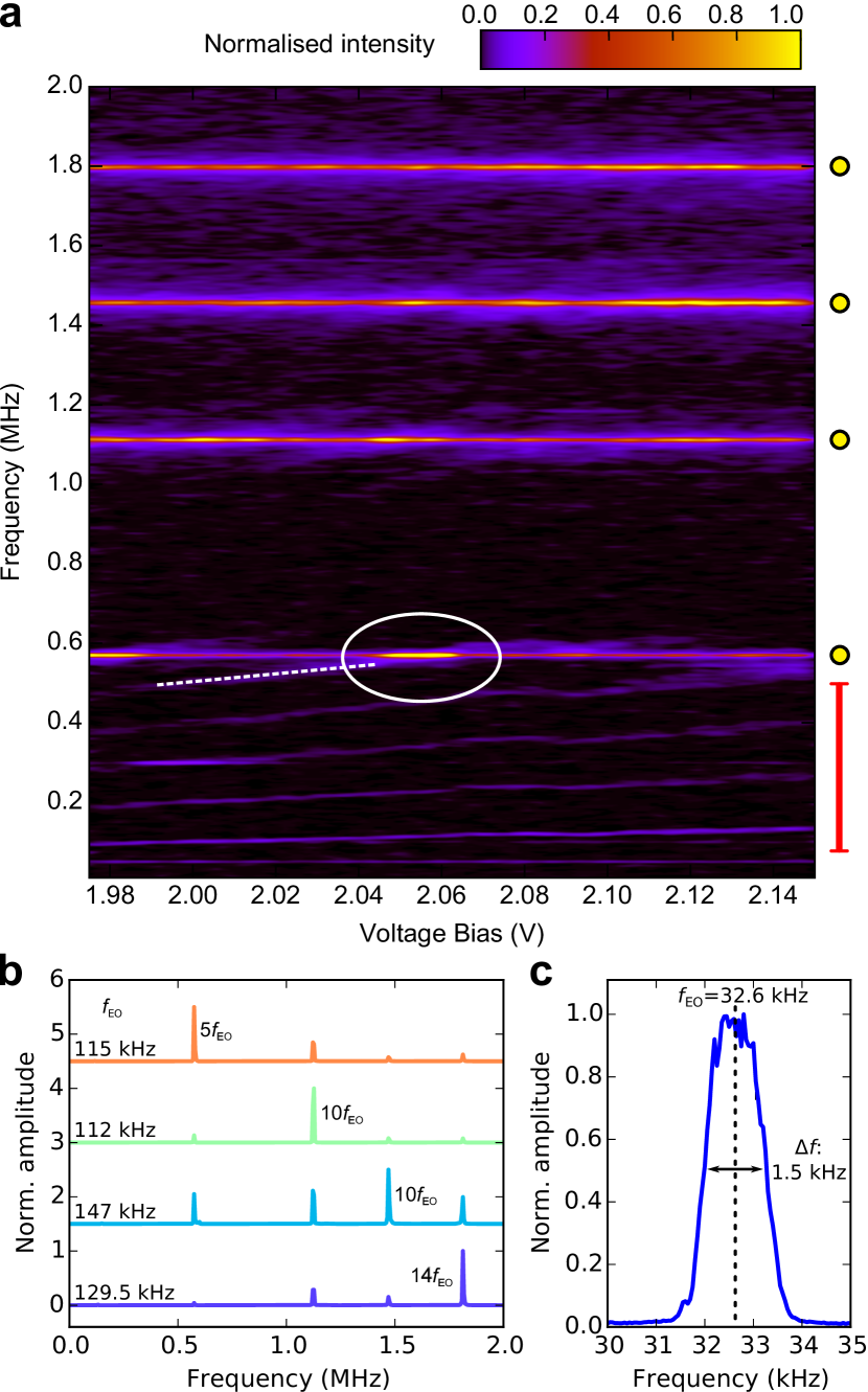
We now demonstrate how the excitation of the different mechanical modes of the microbridge can be controlled by the electrical bias. Fig. 4a shows the power spectra of the deflection of the device measured by the photodiode as a function of , and with fixed . In this configuration, controls the relaxation-oscillation frequency , making our device a spontaneous voltage-controlled electrical oscillator with a gain of about 250 kHz/V. In Fig. 4a, a comb of dim peaks is visible at low frequencies, marked with a red bar. This is an off-resonance response of the device, corresponding to the first few harmonics of the electrical signal of Fig. 2c. By tuning it is possible to match the frequency of one of these harmonic components with a flexural mode of the microbridge (yellow dots). This condition is realized, for example, at the crossing point indicated by the circle in Fig. 4a, where the increase of amplitude of the specific flexural mode is obtained through resonant excitation by the fifth harmonic of the electrical signal, also visible as forced mechanical oscillation in the unmatched condition (white dashed line). The selective excitation of different mechanical modes is achieved by tuning to obtain the desired matching condition, as shown in the spectra of Fig. 4b. The labels indicate the matched harmonic component (n) and the frequency of the selected mode, where, as an example, the 575 kHz peak is excited with the fifth harmonic component of = 115 kHz.
An important characteristic of an oscillator is its frequency stability. In our device the selectivity of the different mechanical modes is determined by the stability of the electrical oscillation. Fig. 4c is an average of 100 acquisitions of the electrical oscillations spectra taken over 40 s for = 32.6 kHz. Its width indicates that the amplitude of the frequency jitter of the electrical oscillations, i.e., their stability over time, is about 4-5 %. This means that even in an unmatched condition, fluctuations of can trigger the resonant actuation of modes close to one of its harmonic components. This explains why in Fig. 4a and b the mechanical modes of the microbridge are slightly visible also in the unmatched condition: as the integration time of the network analyser is much longer than these fluctuations, the instrument shows the averaged mechanical response. The magnitude of the frequency jitter is related to the robustness of the two switching conditions of the \ceVO2 within the gap and may be improved by optimizing device design, growth methods or metal contacts.
In this last paragraph we evaluate the energy efficiency of our device, how it scales with the size of the active region and compare the presented approach with other actuation mechanisms based on self-oscillation in micro and nanostructures. The total amount of energy provided to the system is the total Joule power dissipated in the circuit of Fig. 2a while the electro-thermal oscillations are activated. It can be evaluated by considering that the characteristic of the circuit in Fig. 2b has as upper limit: . Since the load resistor is comparable to the gap resistance in the insulating phase Maffezzoni et al. (2015), as a first approximation this power is evenly split between the microbridge and . The power required to undergo a periodic phase transition of a \ceVO2 volume is the product between frequency and heat absorbed by the transition: , where is the density of \ceVO2, is the latent heat of the transition and is the specific heat of \ceVO2 Cao et al. (2009); Berglund and Guggenheim (1969). For a frequency of 100 kHz, a temperature variation of 10 K and a volume corresponding with the \ceVO2 gap, the resulting average power is about . This value is orders of magnitude below the actual power dissipated in the microbridge, meaning that the power consumption of our device is dominated by thermal dissipations. Several reports in literature discuss the energy efficiency and performances of \ceVO2-based static and quasi-static actuators Wang et al. (2013b); Guo et al. (2013); Cabrera et al. (2014). Here, it is relevant to compare the device power consumption with other self-actuation mechanisms proposed so far. In suspended membranes of 2D materials, for example, it is possible to trigger self-oscillations by focusing a diverging beam of laser light Barton et al. (2012). However, in order to achieve the required light flux gradients to trigger a resonant excitation, several mW of power (>2 mW) are needed. Furthermore, scaling is limited by diffraction, complex optics are necessary and the actuation is not mode-selective. A different approach relies on a self-biasing feedback loop, typically coupled with an electrostatic actuator Feng et al. (2008); Chen et al. (2013, 2016). In this case the power consumption is dominated by the active electronic components in the feedback circuits. Here, a single amplifying elements, as reported in the datasheets of the components used in the experiments, requires at least 1 W of electrical power. In this context, the total power consumption of our \ceVO2-based mechanical actuation mechanism is dramatically lower. Also, since it depends on the volume of \ceVO2 undergoing the phase transition, it scales with the device size, thus foreseeing an enhanced efficiency for nanoscale devices.
In conclusion, we realized a simple and flexible actuation scheme for high-frequency mechanical resonators based on a phase-change material. The intrinsic physical properties of \ceVO2 allow the direct conversion of a small DC voltage into a mechanical excitation in the MHz range without the need of an external driving circuit. This device can be viewed as a spontaneous voltage-controlled oscillator, which is able to selectively excite the different mechanical modes of a microstructure by controlling the bias voltage. Our actuation mechanism can be implemented in a variety of micro-electro-mechanical systems requiring resonant actuation, and the device size can be scaled down to comprise just a single sub-micrometric \ceVO2 domain, allowing individual actuation of nanometric structures. Our approach is thus scalable both in size and number of devices, where multiple micro-/nano-resonators can be actuated in parallel by a single DC source. This opens the possibility of realizing DC-powered arrays of micro-actuators, fast frequency-switching devices or sensors based on multi-frequency detection, with potential applications spanning from micro-robotics to micro-fluidic devices and environmental monitoring.
Methods
Device Fabrication.
The \ceTiO2(23nm) / VO2(90nm) heterostructure is grown on top of a \ceMgO(100) single-crystal substrate by Pulsed Laser Deposition. During the growth the substrate temperature was kept at 450 ∘C and the laser fluency was 18 mJ/cm2. \ceTiO2 is deposited in 0.1 Pa of \ceO2 with a laser repetition rate of 3 Hz, while \ceVO2 in 0.95 Pa of \ceO2 with a repetition rate of 2 Hz. The device is patterned by e-beam lithography using Poly(methyl-methacrylate) resist. \ceTi(5nm)/Au(45nm) electrodes are deposited by thermal evaporation, followed by lift-off in acetone. The bridge geometry is defined by Ar ion milling with an energy of 500 eV and an ion flux of about 0.2 mA/cm2. The structures are suspended by selective etching of the \ceMgO substrate in \ceH3PO4 (8.5 % aqueous solution).
Measurement of mechanical spectrum.
Microbridge motion is detected with a focused laser by an optical lever technique. The laser wavelength is 658 nm and the focused spot size about 2-3 m, well within than the bridge width. The spot is focused at about one fourth of the bridge length, this guarantees a maximum geometric gain of the optical lever. The laser power is kept low in order to minimize additional heating by the laser. This is checked before each measurement by monitoring the electrical resistance of the microbridge with and without the laser on the structure. The device is placed in a vacuum chamber with a Peltier element and a Pt100 thermometer. Sample temperature is controlled with a PID feedback loop and kept fixed at 30 ∘C unless indicated otherwise. All the mechanical spectra have been measured at mbar. The mechanical spectrum of Fig. 1c is measured using a Vector Network Analyser through thermal excitation, by sending a small AC current of , . This current value is well below that needed to drive the phase transition of \ceVO2 in the microbridge.
Reported data.
Measurements reported in Fig. 3 and Fig. 4 have been acquired from different microbridges fabricated on the same sample. Measurements reported in Fig. 4a and Fig. 4b have been acquired in different runs. In Fig. 4a a dim peak is visible at about 50 kHz whose frequency is voltage independent. This signal is due to electronic interference in the photodiode pre-amplifier, and does not affect the measurements. The mechanical power spectra of Fig. 4a are measured using a spectrum analyser from the signal from the photodiode while the electrical oscillations are present. The average of 20 traces is shown, where each trace contains 801 data points, taken across a frequency span of 10 kHz–2 MHz, at a measurement bandwidth of 1 kHz.
Acknowledgements
This work was supported by the Executive programme of cooperation between Italy and Japan by the Italian Ministry of Foreign Affairs, the Dutch Foundation for Fundamental Research on Matter (FOM), a Grant-in-Aid for Scientific Research A (No.26246013), a Grant-in-Aid for Scientific Research B (No.16H03871) from the Japan Society for the Promotion of Science (JSPS).
Author Contributions
N.M and L.P. conceived the experiment. N.M. designed, fabricated and characterized the devices. T.K and Y.H. prepared the \ceVO2/TiO2 heterostructure. W.J.V. assisted with setting up the measurement setup. G.M. provided support in the device fabrication and acquired the SEM images. N.M. wrote the manuscript with the help of L.P. and W.J.V.. H.T., A.D.C. and D.M. supervised the project. All authors discussed the results and commented on the manuscript. N.M. thanks A. Filippetti and D.J. Groenendijk for the useful comments on the manuscript.
References
- Bunch et al. (2007) J. S. Bunch, A. M. van der Zande, S. S. Verbridge, I. W. Frank, D. M. Tanenbaum, J. M. Parpia, H. G. Craighead, and P. L. McEuen, Science (80-. ). 315, 490 (2007).
- Van Thourhout and Roels (2010) D. Van Thourhout and J. Roels, Nat. Photonics 4, 211 (2010).
- Riedinger et al. (2016) R. Riedinger, S. Hong, R. A. Norte, J. A. Slater, J. Shang, A. G. Krause, V. Anant, M. Aspelmeyer, and S. Gröblacher, Nature 530, 313 (2016), arXiv:1512.05360 .
- Castellanos-Gomez et al. (2015) A. Castellanos-Gomez, V. Singh, H. S. J. Van Der Zant, and G. A. Steele, Ann. Phys. 527, 27 (2015), arXiv:1409.1173 .
- Masmanidis et al. (2007) S. C. Masmanidis, R. B. Karabalin, I. de Vlaminck, G. Borghs, M. R. Freeman, and M. L. Roukes, Science (80-. ). 317, 780 (2007).
- Park et al. (2011) J. Park, H. Qin, M. Scalf, R. T. Hilger, M. S. Westphall, L. M. Smith, and R. H. Blick, Nano Lett. 11, 3681 (2011).
- Grover et al. (2011) W. H. Grover, A. K. Bryan, M. Diez-Silva, S. Suresh, J. M. Higgins, and S. R. Manalis, Proc. Natl. Acad. Sci. 108, 10992 (2011).
- Tao et al. (2014) Y. Tao, J. M. Boss, B. a. Moores, and C. L. Degen, Nat. Commun. 5, 3638 (2014), arXiv:1212.1347 .
- Imada et al. (1998) M. Imada, A. Fujimori, and Y. Tokura, Rev. Mod. Phys. 70, 1039 (1998).
- Morosan et al. (2012) E. Morosan, D. Natelson, A. H. Nevidomskyy, and Q. Si, Adv. Mater. 24, 4896 (2012).
- Morin (1959) F. J. Morin, Phys. Rev. Lett. 3, 34 (1959).
- Eyert (2002) V. Eyert, Ann. Phys. 11, 650 (2002).
- Budai et al. (2014) J. D. Budai, J. Hong, M. E. Manley, E. D. Specht, C. W. Li, J. Z. Tischler, D. L. Abernathy, A. H. Said, B. M. Leu, L. A. Boatner, R. J. McQueeney, and O. Delaire, Nature 515, 535 (2014).
- Brockman et al. (2014) J. S. Brockman, L. Gao, B. Hughes, C. T. Rettner, M. G. Samant, K. P. Roche, and S. S. P. Parkin, Nat. Nanotechnol. 9, 453 (2014).
- Kumar et al. (2014) S. Kumar, J. P. Strachan, M. D. Pickett, A. Bratkovsky, Y. Nishi, and R. S. Williams, Adv. Mater. 26, 7505 (2014).
- Driscoll et al. (2009) T. Driscoll, H.-T. Kim, B.-G. Chae, B.-J. Kim, Y.-W. Lee, N. M. Jokerst, S. Palit, D. R. Smith, M. Di Ventra, and D. N. Basov, Science (80-. ). 325, 1518 (2009), arXiv:1003.0140 .
- Kats et al. (2013) M. a. Kats, R. Blanchard, S. Zhang, P. Genevet, C. Ko, S. Ramanathan, and F. Capasso, Phys. Rev. X 3, 041004 (2013), arXiv:1305.0033 .
- Pellegrino et al. (2012) L. Pellegrino, N. Manca, T. Kanki, H. Tanaka, M. Biasotti, E. Bellingeri, A. S. Siri, and D. Marré, Adv. Mater. 24, 2929 (2012).
- Shukla et al. (2015) N. Shukla, A. V. Thathachary, A. Agrawal, H. Paik, A. Aziz, D. G. Schlom, S. K. Gupta, R. Engel-Herbert, and S. Datta, Nat. Commun. 6, 7812 (2015).
- Xiao et al. (2015) L. Xiao, H. Ma, J. Liu, W. Zhao, Y. Jia, Q. Zhao, K. Liu, Y. Wu, Y. Wei, S. Fan, and K. Jiang, Nano Lett. , acs.nanolett.5b04090 (2015).
- Yoon et al. (2016) H. Yoon, M. Choi, T.-w. W. Lim, H. Kwon, K. Ihm, J. K. Kim, S.-Y. Y. Choi, and J. Son, Nat. Mater. 15, 1113 (2016).
- Jenkins (2013) A. Jenkins, Phys. Rep. 525, 167 (2013), arXiv:1109.6640 .
- Taketa et al. (1975) Y. Taketa, F. Kato, M. Nitta, and M. Haradome, Appl. Phys. Lett. 27, 212 (1975).
- Fisher (1978) B. Fisher, J. Appl. Phys. 49, 5339 (1978).
- Gu et al. (2007) Q. Gu, A. Falk, J. Wu, L. Ouyang, and H. Park, Nano Lett. 7, 363 (2007).
- Lee et al. (2008) Y. W. Lee, B. J. Kim, J. W. Lim, S. J. Yun, S. Choi, B. G. Chae, G. Kim, and H. T. Kim, Appl. Phys. Lett. 92 (2008), 10.1063/1.2911745.
- Kim et al. (2010) J. Kim, C. Ko, A. Frenzel, S. Ramanathan, and J. E. Hoffman, Appl. Phys. Lett. 96, 213106 (2010).
- Seo et al. (2011) G. Seo, B.-J. Kim, Y. W. Lee, S. Choi, J.-H. Shin, and H.-T. Kim, Thin Solid Films 519, 3383 (2011).
- Kim et al. (2012) B.-J. Kim, G. Seo, J. Choi, H.-T. Kim, and Y. W. Lee, Jpn. J. Appl. Phys. 51, 107302 (2012).
- Wang et al. (2015) Y. Wang, J. Chai, S. Wang, L. Qi, Y. Yang, Y. Xu, H. Tanaka, and Y. Wu, J. Appl. Phys. 117, 064502 (2015), arXiv:1502.0442 .
- Datta et al. (2014) S. Datta, N. Shukla, M. Cotter, A. Parihar, and A. Raychowdhury, Proc. 51st Annu. Des. Autom. Conf. Des. Autom. Conf. - DAC ’14 , 1 (2014).
- Shukla et al. (2014) N. Shukla, A. Parihar, E. Freeman, H. Paik, G. Stone, V. Narayanan, H. Wen, Z. Cai, V. Gopalan, R. Engel-Herbert, D. G. Schlom, A. Raychowdhury, and S. Datta, Sci. Rep. 4, 4964 (2014).
- Beaumont et al. (2014) A. Beaumont, J. Leroy, J. C. Orlianges, and A. Crunteanu, J. Appl. Phys. 115 (2014), 10.1063/1.4871543.
- Pergament et al. (2016) A. Pergament, A. Crunteanu, A. Beaumont, G. Stefanovich, and A. Velichko, ArXiv , 9 (2016), arXiv:1601.06246 .
- Feng et al. (2008) X. L. Feng, C. J. White, A. Hajimiri, and M. L. Roukes, Nat. Nanotechnol. 3, 342 (2008).
- Unterreithmeier et al. (2009) Q. P. Unterreithmeier, E. M. Weig, and J. P. Kotthaus, Nature 458, 1001 (2009).
- Baek et al. (2011) S. H. Baek, J. Park, D. M. Kim, V. A. Aksyuk, R. R. Das, S. D. Bu, D. a. Felker, J. Lettieri, V. Vaithyanathan, S. S. N. Bharadwaja, N. Bassiri-Gharb, Y. B. Chen, H. P. Sun, C. M. Folkman, H. W. Jang, D. J. Kreft, S. K. Streiffer, R. Ramesh, X. Q. Pan, S. Trolier-McKinstry, D. G. Schlom, M. S. Rzchowski, R. H. Blick, and C. B. Eom, Science (80-. ). 334, 958 (2011).
- Okimura and Furumi (2005) K. Okimura and T. Furumi, Jpn. J. Appl. Phys. 44, 3192 (2005).
- Muraoka and Hiroi (2002) Y. Muraoka and Z. Hiroi, Appl. Phys. Lett. 80, 583 (2002).
- Karabalin et al. (2012) R. B. Karabalin, L. G. Villanueva, M. H. Matheny, J. E. Sader, and M. L. Roukes, Phys. Rev. Lett. 108, 1 (2012), arXiv:1211.0302 .
- Pini et al. (2016) V. Pini, J. J. Ruz, P. M. Kosaka, O. Malvar, M. Calleja, and J. Tamayo, Sci. Rep. 6, 29627 (2016).
- Rua et al. (2010) A. Rua, F. Fernàndez, and N. Sepúlveda, J. Appl. Phys. 107, 074506 (2010).
- Wang et al. (2013a) H. Wang, W. He, G. Yuan, X. Wang, and Q. Chen, Thin Solid Films 540, 168 (2013a).
- Manca et al. (2013) N. Manca, L. Pellegrino, T. Kanki, S. Yamasaki, H. Tanaka, A. S. Siri, and D. Marré, Adv. Mater. 25, 6430 (2013), arXiv:arXiv:1011.1669v3 .
- Liu et al. (2014) K. Liu, C. Cheng, J. Suh, R. Tang-Kong, D. Fu, S. Lee, J. Zhou, L. O. Chua, and J. Wu, Adv. Mater. 26, 1746 (2014).
- Merced et al. (2015) E. Merced, D. Torres, X. Tan, and N. Sepulveda, J. Microelectromechanical Syst. 24, 100 (2015).
- Ma et al. (2017) H. Ma, J. Hou, X. Wang, J. Zhang, Z. Yuan, L. Xiao, Y. Wei, S. Fan, K. Jiang, and K. Liu, Nano Lett. 17, 421 (2017).
- Maffezzoni et al. (2015) P. Maffezzoni, L. Daniel, N. Shukla, S. Datta, and A. Raychowdhury, IEEE Trans. Circuits Syst. I Regul. Pap. 62, 2207 (2015).
- Cao et al. (2009) J. Cao, E. Ertekin, V. Srinivasan, W. Fan, S. Huang, H. Zheng, J. W. L. Yim, D. R. Khanal, D. F. Ogletree, J. C. Grossman, and J. Wu, Nat. Nanotechnol. 4, 732 (2009).
- Berglund and Guggenheim (1969) C. N. Berglund and H. J. Guggenheim, Phys. Rev. 185, 1022 (1969).
- Wang et al. (2013b) K. Wang, C. Cheng, E. Cardona, J. Guan, K. Liu, and J. Wu, ACS Nano 7, 2266 (2013b).
- Guo et al. (2013) H. Guo, K. Wang, Y. Deng, Y. Oh, S. A. Syed Asif, O. L. Warren, Z. W. Shan, J. Wu, and A. M. Minor, Appl. Phys. Lett. 102, 231909 (2013).
- Cabrera et al. (2014) R. Cabrera, E. Merced, and N. Sepulveda, J. Microelectromechanical Syst. 23, 243 (2014).
- Barton et al. (2012) R. A. Barton, I. R. Storch, V. P. Adiga, R. Sakakibara, B. R. Cipriany, B. Ilic, S. P. Wang, P. Ong, P. L. McEuen, J. M. Parpia, and H. G. Craighead, Nano Lett. 12, 4681 (2012).
- Chen et al. (2013) C. Chen, S. Lee, V. V. Deshpande, G.-H. Lee, M. Lekas, K. Shepard, and J. Hone, Nat. Nanotechnol. 8, 923 (2013).
- Chen et al. (2016) C. Chen, D. H. Zanette, J. R. Guest, D. A. Czaplewski, and D. López, Phys. Rev. Lett. 117, 017203 (2016).
See pages 1 of VO2_self_resonator-Supp_info-08_03_2017.pdf See pages 2 of VO2_self_resonator-Supp_info-08_03_2017.pdf See pages 3 of VO2_self_resonator-Supp_info-08_03_2017.pdf See pages 4 of VO2_self_resonator-Supp_info-08_03_2017.pdf See pages 5 of VO2_self_resonator-Supp_info-08_03_2017.pdf See pages 6 of VO2_self_resonator-Supp_info-08_03_2017.pdf See pages 7 of VO2_self_resonator-Supp_info-08_03_2017.pdf See pages 8 of VO2_self_resonator-Supp_info-08_03_2017.pdf See pages 9 of VO2_self_resonator-Supp_info-08_03_2017.pdf See pages 10 of VO2_self_resonator-Supp_info-08_03_2017.pdf See pages 11 of VO2_self_resonator-Supp_info-08_03_2017.pdf See pages 12 of VO2_self_resonator-Supp_info-08_03_2017.pdf See pages 13 of VO2_self_resonator-Supp_info-08_03_2017.pdf See pages 14 of VO2_self_resonator-Supp_info-08_03_2017.pdf See pages 15 of VO2_self_resonator-Supp_info-08_03_2017.pdf See pages 16 of VO2_self_resonator-Supp_info-08_03_2017.pdf