Implementation of a Cost-Efficient Device for Wireless Photon Coincidence Detection
Abstract
State-of-the-art technology for pulse counter electronics offers an important range of commercial devices, but such systems are usually expensive due to the complex logic used for this task. The use of counting electronics in conjunction with photon counters can be used, for example, to perform experimental tests in Quantum Optics and Quantum Information Science. Here, we present the development and implementation of a low cost module for multiphoton coincidence statistics with detection windows of a few nanoseconds. The module consists of an array of logic gates, with a frequency operation of 250 MHz that corrects and amplifies the detectors signal. The device characterisation was done by means of detection of Transistor-Transistor Logic (TTL) signals retrieved from a signal generator, and implemented in an optical setup. The detected output signals (TTL pulses) were analysed and stored in a computer by means of a Field Programmable Gate Array (FPGA). Our module incorporates fundamental electronics that is currently used in the first experimental proof-of-principle tests in quantum information and molecular spectroscopy at CIBioFi.
1 Introduction
In less than three decades, a new technological revolution has been boosted by harnessing the fundamental principles of quantum mechanics, and the superposition and entanglement of quantum states have been at the core of such a development. This, however, implies a big challenge for testing and implementing remarkable protocols such as quantum computation, cryptography, and teleportation in quantum information science [1, 2, 3, 4]. In the case of optical technologies, the detection of individual pulses and photon-coincidences is fundamental [5, 6], and setups for Light Detection and Ranging (LIDAR) [7], Fluorescence Correlation Spectroscopy (FCS) [8, 9], molecular life-time emissions and quantum entanglement and correlations quantification [9, 10, 11], between others, rely on this feature in a crucial way. Thus, photon statistics [12, 13, 14] through the coincidence counting (detection of photons-simultaneously or within a small time window) provide a key ingredient in Science and Engineering.
Most of the time-dependent statistics of photons in different experimental schemes has been made possible thanks to a Time to Amplitude Converter (TAC) protocol, which allows for the measurement of the time interval between incident pulses, from “start” to “stop”, and generates an output pulse that is proportional to this time interval. This action is commonly implemented in experimental setups used for the characterisation of molecular systems such as “Time Correlated Single Photon Counting” (TCSPC) [15, 16]. This said, such a protocol for coincidence counting of multiple photons is nowadays expensive and easily saturable due to the long dead-time intervals around 8 MHz in reverse mode operation [17], and even for 16 MHz [18].
Time-to-Digital Converter (TDC) is another procedure that employs the “start-stop” principle. This can be entirely implemented on a digital basis, thus avoiding the use of ADC (Analog-to-Digital) protocols that limit TDC applications to sub-micron technologies [19]. Current TDC technology could achieve a maximum frequency in the 5-10 GHz range and reach a maximum around 200 ps for the measurement accuracy [20], and even a shorter sampling time [21, 22, 23]. Combining this technique with photon detectors such as the Avalanche Photodiode (APD), the sampling would be limited by the maximum rate allowed by the detector. This method can be employed in diverse experiments, ranging from, e.g., materials surface reconstruction in the measure of the Time-of-Flight (ToF) of photons from a transmitter to a target and back to the detector [24], fluorescence life-time imaging [25], to TCSPC [21, 26]. Thus, a purely digital proposal which offers an appropriate sampling rate at a reduced implementation cost [6, 27, 28] can be very useful for the purpose here developed.
2 Experimental Development
2.1 Counting module assembly
In 2009, Branning et al. [6] posed to change the TAC protocol by implementing a set of logic gates. This assembly used a TTL pulse sent by a commercial photo counter to modify the pulse width, then defined the coincidence, and finally used a Peripheral Interface Controller (PIC) to count and store the data in a computer. After this, the PIC was replaced by a Field Programmable Gate Array (FPGA) that developed the same functionality as its predecessor but became better suited and adaptable [27]. This development is appealing due to the cost-efficiency of these devices, and besides, this also allows the scalability to 4 inputs but using different Coincidences Counting Modules (CCM) [28].
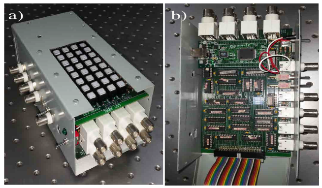
We initially used a third generation proof board of Branning’s CCM [29] and assembled a device as shown in figure 1. This CCM was built on electronic boards of four layers each one. In one of them, we located the different electronic devices, NANDs, ORs, and Multiplexors. In the second card, the manual selection of input signals and the hosting of switches was configured, as can be seen in figure 1(a), and 1(b). Those devices are protected by a metallic box to preserve their electronic components, and to allow for an easier manipulation of the counting module. The main limitation of this module, however, is the reduced number of inputs (4) for the Single Photon Counting Modules (SPCM), given that, for example, state-of-the-art quantum optics experiments can entangle up to ten photons, and use around 20 APDs for their detection [14]. In this sense, recent efforts have expanded other counting strategies with different techniques that are able to reach up to 32 [8], and even 48 inputs [30].
In this work, we report the implementation of a photon-counter coincidence module with a short response time (a few ns), and use as a counting device an FPGA DE0-nano model [31]. In this module, we expand Branning et al. initial proposal, by increasing the number of inputs up to 8 as well as the coincidences (8-fold). In our implementation, we used integrated circuits of fast series (SN74FXXX) of different logical arrays, and a wireless module to communicate the data to a software analyser. The stages followed in the coincidence counting process are as follows: i) pulse shaping, ii) selection of the input signal, iii) counting, and iv) storing the acquired data. We next describe these steps.
2.2 Shaping the input pulses
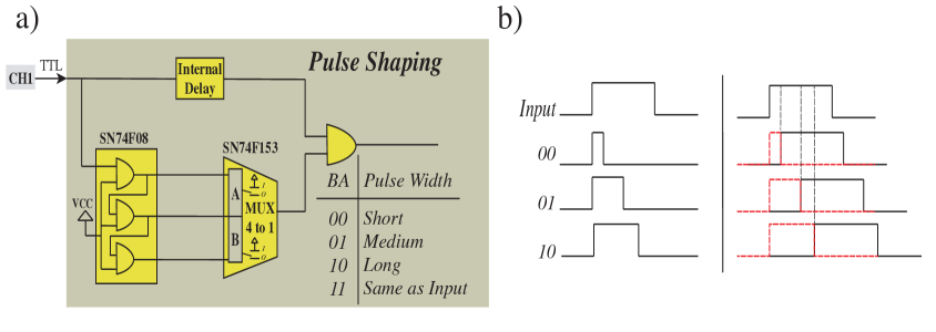
A description of the pulse shaping process is schematically given in figure 2(a). First, the signal splits into two equal and temporal synchronised signals, next both of them are delayed but subjected to the following two-path rule. In the upper path, the delay is controlled through a double inverter logic circuit which is equivalent in time to the application of two digital gates. In the lower path, the delay is defined by the selectors and , where “” and “” denote off and on states, respectively. This delay finally defines the width of the output pulse, as is shown in figure 2(b).
2.3 Selecting the input signal
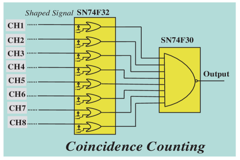
All the input pulses are shaped as explained before but only the modules’ user defines the number of inputs that are to be considered in the coincidence process. The selection of the signals is implemented via a switching system that allows the following: to select a channel (or channels) for detection and counting the pulses, and then, counting the coincidences between signals. Each shaped input is compared with the logic state of a switch (“0” or “1”) through an OR-gate (SN74F32), and the logic result is transmitted to the coincidence channel performed by an AND-gate (SN74F30), as is sketched in the figure 3, to be finally counted. The coincidence protocol is just the logical comparison of the selected pulses in a defined time interval (a few ns) through an AND-gate. To sum up, the definition of a coincidence is limited by the electronics logical response time at the gate, and by the number of followed buffers.
2.4 Counting, saving and data acquisition
For this purpose, the final pulses are counted and stored for later acquisition in readable files in a computer. This is developed by means of an FPGA of programmable logic and connections under VHSIC222Acronym for Very High Speed Integrated Circuits Hardware Description Language (VHDL). A MORPH-1C-II system [32] has been recently introduced, in four channels protocols [29], due to its Multi Protocol Synchronous Serial Engine that allows programming and re-programming by means of a USB port in a fraction of a second, i.e., of at least s [33]. This implementation, however, has a practical drawback since it requires programming every time that a lack of power supply arises and, operatively speaking, a plug-&-play usage with this kind of FPGA is not possible. Another hurdle arises from this model’s processing capability due to the fact that an increment in the number of possible input signals implies an increment of the number of selecting switches, as shown in figure 1(a) and figure 3. As an alternative, this switching system can be included in a software interface using the logical elements of the FPGA instead of hardware buttons. In the latter, an FPGA with a larger number of logical elements is to be required.
In our implementation, we resort to an FPGA with a ROM memory for the counting process as the DE0 nano [31] from the Cyclone™IV family [33]; this device has two headers of 40 pins each one, where 72 pins are input/output, 4 power pins, and 4 GND pins; connection to a USB port for its output signals and 23 pins for connection to a JTAG interface (standard protocol to develop debugging tools [34]). Another key feature of this model is the maximum acceptable frequency of for the input signals, and a larger number of logical elements: compared to of the MORPH-1C-II. These features allow the detection of different physical systems that range from the single photon counting and coincidences through to the radioisotopes in positron emission tomography [35].
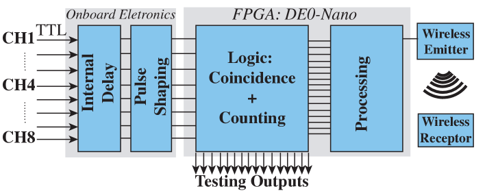
For programming this FPGA, we used the compilation environment Quartus™. The particular code used here can create eight registers of independent counts of 16 bits available each one to define the channel of the register. This number of channels stems from the module inside that compares the selected input signals between them to count coincidences in the FPGA. To obtain the saved data, we used XBee modules that allow the wireless communication between the FPGA and a designated computer [36]. This process relies on the time needed to send the data by the transmission module (). In order to overcome lacks in the processing, it is useful to define integration times to count in the FPGA in the same order (). The required variables in the process of wirelessly data sending are the sending rate (number of data send per second) and the bit length (“size” of the data), which depend on the number of channels to count. These variables determine the file transmission and reception, and are set in the code that is implemented within the FPGA and the XBee (XCTU) module. Finally, the file arrives to a reception module that is connected to a computer to visualise and analyse the counts, as schematically shown in figure 4.
2.5 Device estimated cost
The total cost involved in the construction of the coincidence counting device can be estimated as follows: i) FPGA DE0-nano USD, ii) PCBs (assembling cards) USD, iii) the complete set of fast series circuits (SN74FXXX) USD, iv) additional electronics and housing (switches, cables, LEDs, BNC connectors, metallic box) USD. These give an approximate total of about USD. This is to be contrasted with typical commercial devices available in the market (with similar features) that can be well above USD (e.g., Canberra Model 2040 and National Instruments modules).

3 Device Response and Discussion
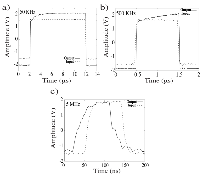
The coincidence counting module was carefully checked in each one of the previously mentioned stages. The pulses used for testing this module were generated by a square pulse generator set at three different frequencies (50 KHz, 500 KHz, and 5 MHz). As mentioned before, the input pulses can be modified in their temporal widths by using different configurations of the selectors in the MUX of the pulse shaping stage. In this sense, the short width of the pulse is reached in the configuration “”, and the minimal modification over the input signal should be obtained in the “” configuration.
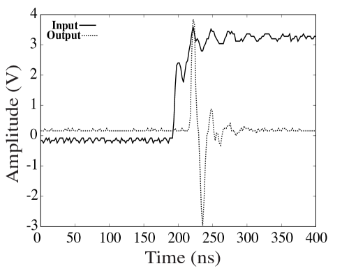
In figure 5 we show the effect of the pulse shaping in the configuration “” over a square input signal in the counting module. Here, we observe that the output exhibits a damped oscillator-like behaviour, possibly due to the response time at the logic circuits. This input signal has a frequency of , which means an average width of , and the shaping process produces an output of ; this represents a reduction of at least five orders of magnitude of the former width. Although the plot shows a delay of a few nanoseconds between the input and the output signals, this difference is comparably small: % of the input pulse width. We also verified the output signal in the configuration “”, and were able to find an increment in the amplitude when compared to the input pulse, as can be seen in figure 6.
This could be achieved due to the amplification performed by the shaping electronics at this stage and the impedance of the cables used for this experiment. However, this amplification process takes a time comparable to the time scale of these inputs to reach a maximum value. This behaviour is responsible for the ‘round corner’ in the amplification output in figure 6(a). When the frequency is changed, say by one order of magnitude, the shaping, initially rounded, is modified to a triangular-like shape, as shown in figure 6(b). This means that the amplification procedure is slower than the period of the input signal, and the maximum amplitude is not reached before the temporal width vanishes. In addition, frequencies in the range of MHz exhibit an alteration of the output pulse and a “non-evident” voltage amplification process. For the case of a 5 MHz input signal, an apparent earlier appearance of the output (with respect to the input) signal is observed in figure 6(c). We estimate the uncertainty due to this time shift presented by the output signal at FWHM around % of its width. This is due to the usage of an oscilloscope’s trigger signal that did not allow us to produce a proper compensation of the output signal.
This visualisation issue, however, does not compromise the functioning of the counting device, since the amplifying response during the shaping stage does not affect the efficiency of the counting process due to the fact that the counting frequency is proportional to the input frequency, as shown in figure 7. We found that, in the configuration “”, the frequency of the input signal is proportional to the counting frequency by a constant value . The “” configuration exhibits a likewise proportionality with a very similar constant.
4 Concluding Remarks
We have built a cost-efficient (compared to commercial prices) counting module device of eight inputs, as well as eight-fold coincidence channels that exhibit key features that can be used in different areas of science, engineering and the medical sciences, and in particular, in quantum and non-linear optics. These features allow us to perform a more in depth analysis about incident photons in quantum optics and quantum information experiments. The reported counting module has a response time of a few nanoseconds and works for incident signals with frequencies up to 150 MHz. This module is currently being implemented in our laboratory for the detection of Werner-like states which have recently been proposed as a novel resource for quantum game strategy in a protocol that requires neither quantum entanglement nor nonlocality as a resource [4]. We work on the FPGA programming to improve the module for data transfer in quantum tomography of one and two polarisation photonic qubits experiments.
The device here implemented for photon coincidence detection shall also be used in quantum interferometry, and photo-luminiscence detection in molecular spectroscopy experiments.
Acknowledgments
E.I. thanks the “Virginia Gutierrez de Pineda Young Researcher and Innovator” COLCIENCIAS programme. We would like to thank Universidad del Valle (grant 7930), COLCIENCIAS (grant 71003), and Fondo CTeI-Sistema General de Regalías (contract BPIN 2013000100007) for financial support.
References
- [1] J. Preskill, Quantum Computation Lecture Notes. Caltech, 2016.
- [2] M. A. Nielsen and I. L. Chuang, Quantum Computation and Quantum Information: 10th Anniversary Edition. Cambridge University Press, 2010.
- [3] Y.-H. Kim, S. P. Kulik and Y. Shih, Quantum teleportation of a polarization state with a complete bell state measurement, Phys. Rev. Lett. 86 (2000) 1370 – 1373.
- [4] C. A. Melo-Luna, C. E. Susa, A. F. Ducuara, A. Barreiro and J. H. Reina, Quantum locality in game strategy, Sci. Rep. 7 (2017) 1.
- [5] S. Gaertner, H. Weinferter and C. Kurtsiefer, Fast and compact multichannel photon coincidence unit for quantum information processing, Rev. Sci. Inst. 76 (2005) 123108.
- [6] D. Branning, S. Bhandari and M. Beck, Low cost coincidence-counting electronics for undergraduated quantum optics., Am. J. Phys. 77 (2009) .
- [7] M. Chevrier and G. Campanella, How to build a lidar system with a time-to-digital converter, Analog App. Journal 1Q (2017) 1.
- [8] S. Gong, I. Labanca, I. Rech and M. Ghioni, A 32-channel photon counting module with embedded auto/cross-correlators for real- time parallel fluorescence correlation spectroscopy, Rev. Sci. Inst. 85 (2014) 103101.
- [9] W. Becker, ed., Advanced Time-Correlated single Photon counting Applications, vol. 111 of Springer Series in Chemical Physics. Springer, Switzerland, 2015.
- [10] C. E. Susa and J. H. Reina, Nonlocal fluctuations and control of dimer entanglement dynamics, Phys. Rev. A 82 (2010) 042102.
- [11] C. E. Susa and J. H. Reina, Correlations in optically controlled quantum emitters, Phys. Rev. A 85 (2012) 022111.
- [12] P. G. Kwiat and J. B. Alteper, Optical technologies for quantum information science, Proc. SPIE, Quantum Communications and Quantum Imaging 5161 (2004) .
- [13] C. Spengler and M. Huber, Entanglement detection via mutually unbiased bases, Phys. Rev. A 86 (2012) 022311–1.
- [14] X.-L. Wang, L.-K. Chen, W. Li, H.-L. Huang, C. Liu, C. Chen et al., Experimental ten-photon entanglement, Phys. Rev. Lett. 117 (2016) 210502.
- [15] S. Antonioli, L. Miari, A. Cuccato, M. Crotti, I. Rech and M. Ghioni, 8-channel acquisition system for time-correlated single-photon counting, Rev. Sci. Inst. 84 (2013) 064705.
- [16] W. Becker, The bh TCSPC Handbook. Becker & Hickl GmbH, Nahmitzer Damm 30, 12277 Berlin, sixth ed., December, 2014.
- [17] J. R. Lakowicz, Principles of Fluorescence Spectroscopy. Springer, Center for Fluorescence Spectroscopy, University of Maryland School of Medicine, Baltimore, third ed., 2010.
- [18] M. Crotti, I. Rech and M. Ghioni, Four channel, 40 ps resolution, fully integrated time-to-amplitude converter for time-resolved photon counting, IEEE J. Solid-State circuits 47 (March, 2012) 699.
- [19] M. Lampton and R. Raffanti, A high-speed wide dynamic range time-to-digital converter, Rev. Sci. Inst. 65 (November, 1994) 3577.
- [20] S. Henzler, Time-to-Digital Converters. Springer Series in Advanced Microelectronics 29. Springer, Lehrstuhl für Technische Elektronik Arcisstr. 21, 80290 München, Germany, 2010.
- [21] New Circuits and Systems Conference (NEWCAS), 2014 IEEE 12th International, 10-ps resolution hybrid Time to Digital Converter in a 0.18 CMOS technology, (Trois-Rivieres, QC, Canada), IEEE, October, 2014.
- [22] M. Zhang, H. Wang and Y. Liu, A 7.4 ps fpga-based tdc with a 1024-unit measurement matrix, Sensors 17 (February, 2017) 18.
- [23] J. Song, Q. An and S. Liu, A high-resolution time-to-digital converter implemented in field-programmable-gate-arrays, IEEE Transactions on Nuclear Science 53 (February, 2006) 236.
- [24] I. Vornicu, R. Carmona-Galan and A. Rodriguez-Vazquez, A cmos imager for time-of-flight and photon counting based on single photon avalanche diodes and in-pixel time-to-digital converters, Romanian Journal of Information Science and Technology 17 (2014) 354.
- [25] R. M. Field, S. Realov and K. L. Shepard, A 100 fps, time-correlated single-photon-counting-based fluorescence-lifetime imager in 130 nm cmos, IEEE J. Solid-State circuits 49 (April, 2014) 867.
- [26] B. Markovic, S. Tisa, F. A. Villa, A. Tosi and F. Zappa, A high-linearity, 17 ps precision time-to-digital converter based on a single-stage vernier delay loop fine interpolation, IEEE Trans. Circ. Syst.—I 60 (March, 2013) 557.
- [27] D. Branning and M. Beck, An fpga-based module for multiphoton coincidence counting, Proc. SPIE, Advanced photon Counting Techniques VI 8375 (2012) .
- [28] D. Branning and S. Khanal, Note: Scalable multiphoton coincidence-counting electronics, Rev. Sci. Inst. 82 (2011) 016102.
- [29] D. Branning, “Private communication.”
- [30] C. Zhang, W. Li, Y. Hu, T. Yang, G. Jin and X. Jiang, 48-channel coincidence counting system for multiphoton experiment, Rev. Sci. Inst. 87 (2016) 113107.
- [31] Terasic technologies, HsinChu, Taiwan, DE0-Nano user manual, v2.0 ed., 2013.
- [32] Future Technology Devices International Ltd (FTDI), Centurion Business Park, Glasgow, United Kingdom, Morphi-IC-II Datasheet, 1.04 ed., 2011.
- [33] Altera Corporation, San Jose, CA 95134, USA, Cyclone IV Device Handbook, 2016.
- [34] K. Posse, 1687-2014 IEEE Standard for Access and Control of Instrumentation Embedded within a Semiconductor Device. IEEE Computer Society, 2014.
- [35] G. B. Ko, H. S. Yoon, S. I. Kwon, S. J. Hong, D. S. Lee and J. S. Lee, Development of fpga-based coincidence units with veto function, Biomed. Eng. Lett. 1 (2011) 27 – 31.
- [36] MaxStream Inc., 355 South 520 West, Suite 180, XBeeTM/XBee-PROTM OEM RF Modules, m100232 ed., 2007.