The effects of Moiré lattice on the electronic properties of graphene.
Abstract
We study structural and electronic properties of graphene grown on SiC substrate using scanning tunneling microscope (STM), spot-profile-analysis low energy electron diffraction (SPA-LEED) and angle resolved photoemission spectroscopy (ARPES). We find several new replicas of Dirac cones in the Brillouin zone (BZ). Their locations can be understood in terms of combination of basis vectors linked to SiC 6 6 and graphene reconstruction. Therefore these new features originate from the Moiré caused by the lattice mismatch between SiC and graphene. More specifically, Dirac cones replicas are caused by underlying weak modulation of the ionic potential by the substrate that is then experienced by the electrons in the graphene. We also demonstrate that this effect is equally strong in single and tri-layer graphene, therefore the additional Dirac cones are intrinsic features rather than result of photoelectron diffraction. These new features in the electronic structure are very important for the interpretation of recent transport measurements and can assist in tuning the properties of graphene for practical applications.
I Introduction
In the last decade, graphene has become a topic of intense research because of its unique structural and electronic properties such as presence of Dirac dispersion, which leads to high thermal conductivity Balandin et al. (2008), ballistic transport Du et al. (2008), and ultrahigh electron mobility Bolotin et al. (2008). Each carbon atom has a -bond perpendicular to the graphene plane. These bonds are jointly hybridized to form -bands and * bandsCooper et al. (2012). Graphene can be readily grown on large area insulating, semiconducting and metallic substrates. Lattice mismatch at the substrate interface leads to the formation of Moiré patterns (i.e. a superlattice) with larger periodicity than the lattice constants of each of the two separate lattices. This is a standard way to obtain weak periodic potentials superimposed on the graphene potential with characteristic periodicity of several nanometers. The strain caused by lattice mismatch is one of important ways to tune the graphene electronic structure and properties Park et al. (2008a, b); Ponomarenko et al. (2013); Decker et al. (2011). Recently, tuning the periodicity of the ionic potential experienced by electrons in graphene grown on boron nitride substrate and measuring its fractional quantum Hall resistance enabled the engineering of the energy spectrum of Hofstadter butterfly Hofstadter (1976); Dean et al. (2013); Hunt et al. (2013); Yu et al. (2014); Wang et al. (2015).
Silicone carbide (SiC) is one of the most common substrates to grow graphene because of its hexagonal crystal structure with lattice constant aSiC = bSiC = 3.073 Å, c = 10.053 Å. The 6H-SiC consists of Si-C bilayers that are stacked in the pattern of ABCACBHass et al. (2008). Because of different lattice constants of SiC and graphene, when graphene is grown, an intermediate layer will be constructed at the SiC surface between substrate and graphene. This intermediate layer may exhibit rotational disorder, forming Moiré patternsBommel et al. (1975); Forbeaux et al. (1998).
Epitaxial graphene grown by thermal annealing of SiC has been studied extensively with several complementary techniques to reveal its structural and electronic properties. These studies helped to better understand many aspects of graphene layer on SiC (ionic center position, thickness uniformity, stacking, relative layer orientation and variation of the band structure with number of graphene layers) Bommel et al. (1975); Starke et al. (1997); Forbeaux et al. (1998); Lauffer et al. (2008); Hass et al. (2008); Xu et al. (2014); Ohta et al. (2007). However, a number of questions still remain about the nature of the graphene-substrate interface and how it affects the Dirac fermions. The layer at the interface, referred to as the “buffer” or “zeroth” layer graphene, has no -bandsVarchon et al. (2007). This layer increases the carrier concentration and shifts the Femi level, without modifying the shape of the Dirac cones Varchon et al. (2007). Structurally, the buffer layer was represented in terms of the two coincidence lattices, which form two distinct diffraction patterns: (1) 6 6 (oriented along the SiC unit cell) and (2) rotated 30⋅ from the 6 6 unit cell. A new type of buffer layer was grown with linear -bands separated by a measurable gap Zhou et al. (2007). This study motivated new experiments to correlate structural and electronic information necessary for understanding and controlling the properties of graphene. The surface reconstruction has been studied by several techniques in the past, including LEED Bommel et al. (1975); Forbeaux et al. (1998); Starke et al. (1997), auger electron spectroscopy Bommel et al. (1975); Starke et al. (1997), scanning tunneling microscope Starke et al. (1997); Xu et al. (2014) and ARPES Ohta et al. (2007); Bostwick et al. (2006); Ohta et al. (2006); Bostwick et al. (2007); Mucha-Kruczyński et al. (2008); Ohta et al. (2008); Zhou et al. (2008); Gierz et al. (2011); Walter et al. (2011); Ohta et al. (2012); Nevius et al. (2015). Coincidence lattices have been used routinely to probe buried interfaces and deduce information about geometric or electronic corrugationsEmtsev et al. (2008).

The structure of the buffer layer is still an open question. The first detailed work explored this using LEED and STM and proposed a commensurate model based on the Si-dangling bonds Emtsev et al. (2008). The electronic structure of this model was predicted to be insulating. Recent work Ohta et al. (2012) has shown that the buffer layer can be semiconducting if the right annealing conditions are followed with a small gap opening up. This was shown to be related to a hidden incommensurate structure present in the buffer layer and that the structure of the buffer layer is strongly coupled to the SiC bilayerConrad et al. (2017). Additional ARPES and STM work has mapped out the initial stage of the buffer layer and the corresponding changes to the band structure. The work has shown that the small gap is seen to evolve from the initial electronic features of the buffer layer to the semiconducting phase with the 6x6 SiC periodicity visible in constant energy ARPES maps N. Nair et al. (2017). Our work shows the same three Dirac replica cones for both monolayer and trilayer. The cones are defined by the same 6x6 sublattice reciprocal lattice vectors so it is consistent and complement the previous measurements Rotenberg and Bostwick (2015). It is very puzzling why even after the graphene layer is complete the key remaining wavevectors are the 6x6 and not the 13x13 despite the graphene layer becoming uniform. It was also shown Riedl et al. (2009) that hydrogen intercalation of decouples the graphene layer from the substrate.
Here we focus on the 6x6 reconstruction that marks the onset of formation of the buffer layer and it remains present even after additional graphene layers are grown. This reconstruction leads to appearance of new features in the electronic structure, namely additional replicas of the Dirac cones. The photoelectron intensity of these objects does not decrease with increasing number of graphene layers and each replica has very different pattern of intensities rapidly changing with momentum and binding energy. This demonstrates their intrinsic origin, rather than trivial photoelectron diffraction. In fact, the pattern of the band dispersion within these replica cones and the corresponding wavevectors they appear at, prove that they arise due to weak modulation of the electronic potential of graphene. The modulation is caused by the interplay of lattice periodicities, i. e. formation of Moiré pattern. This modulation of the graphene potential is very relevant to recent transport results and provides a pathway for understanding its properties.
II Experimental Details
We use commercial 6H-SiC substrate to grow graphene. We first anneal the 212 mm substrate at 600 ∘C for 3 hours to clean its surface and then increase the temperature of the SiC to 1200 ∘C for 10 minutes. This procedure results in a growth of a single layer of graphene, as confirmed by STM, LEED and ARPES. Tri-layer graphene is grown by heating up the same sample for another 10 minutes at 1200 ∘C. ARPES measurements were performed at Ames Laboratory using a high precision ARPES spectrometer that consists of a Scienta SES2002 electron analyzer and a GammaData Helium UV lamp equipped with custom designed refocusing optics. All data were acquired using the HeI line with a photon energy of 21.2 eV. The angular resolution was 0.13∘ and 0.5∘ along and perpendicular to the direction of the analyzer slits, respectively. The energy corresponding to the chemical potential was determined from the Fermi edge of a polycrystalline Au reference in electrical contact with the sample. The energy resolution was set at 20meV - confirmed by measuring the energy width between 90% and 10% of the Fermi edge from the same Au reference. The data were measured using several samples yielding consistent results.
| D1 | D2 | D3 | |
|---|---|---|---|
| Calculated position (in units of K distance) | 0.230 | 0.384 | 0.615 |
| Measured position | 0.240 | 0.390 | 0.619 |
| Error (%) | 4.3 | 1.6 | 0.7 |
III Results and Discussion
Figure 1a shows the topography of graphene layer measured by STM. Clear Moiré pattern is visible as periodic “checkerboard”-like pattern. The intensity variations are due to the combination of the periodic changes in layer height and electronic densities. A small rhombus is used to outline the 6 6 “quasi cell”. Figure 1b shows the Fourier transform of 1a. The bright points in white circles are due to the lattice modulation. This data is consistent with the result of SPA-LEED shown in Figure 1c. The zero order spot is located at the center of the image and surrounded by six “” spots. The first order diffraction peaks from SiC are surrounding the center peak with smaller radius. The graphene first order peaks are further away and rotated by 30∘ from the SiC pattern. Each of the diffraction peaks is surrounded by six “” spots as expected. The ratios of the positions of graphene and SiC first diffraction spots is 1.26, are consistent with ratios of their respective reciprocal lattice constants (3.08 : 2.46). In between zeroth and first order diffraction peaks of graphene there are four additional, weaker peaks due to the lattice modulation. A schematic drawing of all observed diffraction peaks is shown in Figure 1d based on data in panels (b) and (c). Vectors S1 and S2 are pointing to SiC reciprocal points, while vectors G1 and G2 are of graphene layer. All other points arise due to combinations of the S and G vectors. For example, vector is obtained as G1 + G2 - 2S1 and points to one of the six satellite peaks around the center. In defining the four vectors , , , it is important to define the lattice constants of the two unit cells of the 6 6 and coincidence lattices. If we use the graphene BZ (BZ = ) as 100 then the 6 6 reciprocal space unit cell has a magnitude BZ and the reciprocal space unit cell has a magnitude BZ. Peaks , , in the diffraction pattern of Figure 1d can be written in terms of vectors along the 6 6 reciprocal lattice directions which are multiples of , added to fundamental spots. Point is separated by a vector of magnitude from (0, 0), point is separated by a vector of magnitude 6 from fundamental spot G1 - G2 and point is separated by 6 from fundamental spot G2. On the other hand the point belongs to the reciprocal lattice of the coincidence lattice at positions 5 measured from (0, 0). The origin of the vector has been debated in the literature over long time (both in the more recent case of graphene and the older literature discussing thermal annealing of SiC to form graphite in terms of being incommensurate spots or as spots originating only from multiple scattering). Our recent high resolution SPA-LEED measurements indicate that the leads to strongest diffraction spots of the coincidence 6 lattice. These spots are present only when the buffer layer and first layer graphene form. On the other hand the spots corresponding to vectors , , are still present even when multilayer graphene is grown.
The replicas of the main Dirac cones observed in ARPES data, described by a set of above mentioned vectors, are shown in 1e. The three replica cones originate from the three vectors , , measured from the corner of the BZ . They are related to the corresponding wavevectors of the LEED pattern in Fig. 1d if the LEED vectors are translated by the vector . The three vectors are separated by (the vector), 1.666 () and 2.666 (), respectively, measured from . The vectors and are symmetrically located about the midpoint of the side and their separation is . When they are compared to the experimental ratios seen in Fig. 2 (a) and in Table 1 (normalized to the length of , 4.33) they result in ratios 0.23 for , 0.384 for and 0.615 for , which are in excellent agreement with the measured values 0.24 for , 0.390 for and 0.619 for . Furthermore if the vectors and are measured from the opposite corner of (by adding 4.33), they correspond to vectors 6 (4.33 + 1.66) and 7 (4.33 + 2.66). All wavevectors for the three replicas seen in the current experiments are the same as the replicas seen in ref. Nevius et al. (2015) (the first replica closest to the BZ was measured from the original corner so it corresponds to a separation of ). In ref. Nevius et al. (2015) only the buffer layer was grown but the current work shows that they are the relevant vectors, even for much thicker graphene. A fainter spot is seen at D4 with wavevector which becomes extinct in the LEED pattern after the monolayer is complete. The green first Brillouin zone border is the same as in Fig. 1d.

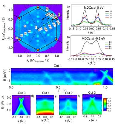
The plot of ARPES intensity at EF for a single layer graphene grown on SiC is shown in Figure 2a and is based on a measurement over one sixth of the Brillouin zone and symmetrization. In addition to the “main” Dirac cones at the corners of the BZ, there are several replicas of the main Dirac cones shifted by a set of vectors from the K point. Namely, there are three replicas along each symmetry line connecting the center and corners of the BZ and are located at 0.240, 0.390, 0.619 from K point. The = = 0.983 Å-1 is the distance between point and K point in the graphene’s first Brillouin zone. The location of each of the replicas can be constructed as a combination of the first order diffraction vectors of the graphene and SiC lattices as explained in 1e. Therefore, each main Dirac cone D0 is surrounded by three sets of 6 replicas Dirac cones. Taking Dirac cone D0 at K1 as an example, it has one replica at D1s (D1 and its 6-fold symmetry points) (vector v1), two replicas at D2s (vector v2 and v2’), and three replicas at D3s (vector v3, v3’ and S1) which can be written as v3+v3’ within first BZ. The obvious mechanism for creating such signal in ARPES is photoelectron diffraction, however our data demonstrates that this is not the case here: this effect is due to the weak modulation of the ionic potential in the graphene layer caused by the interface with the substrate. This weak modulation of the potential is “felt” by conduction electrons as perturbation of the graphene periodic ionic potential. Such effect is quite important as it likely impacts the transport properties of graphene grown on SiC substrates.
The band dispersion along the - K symmetry direction is shown in Figs. 2b. Figure 2c-f show the band dispersion along cuts perpendicular to the symmetry axis - marked in panel (a). The main Dirac cone consists of a single band, a clear signature of a single-layer graphene Ohta et al. (2007). The intensity of each Dirac replica is significantly weaker but still clearly visible on top of the background with D3 being the strongest and D1 the weakest. The shapes of replica dispersions D1 - D3 are identical to D0. The momentum distribution curves (MDC’s) at the and -0.8 eV are shown in panels (g) and (h), respectively. The separation of the MDC peaks at EF is very similar demonstrating close relation between main cone D0 and replicas D1,D2 and D3.

Figure 3a shows the Fermi surface of a three-layer graphene. The replica cones are at the same positions as in single-layer graphene. Their crossections have slightly different shapes than the ones in Fig. 2(a), which may be due to additional sheets of FS originating from three atomic layers of graphene. Fig. 3b shows constant energy contours at 0.8 eV below the Fermi level for the main Dirac cone and the three replicas. The main Dirac cone and D1 have an oval crossection with long axis being horizontal (i.e. along - K ). This is because the vector connecting them is parallel to the - K symmetry direction. D2 and D3 cones also have an oval shape, but are oriented perpendicular to the - K . This is because they are connected with translation vectors to the adjacent main Dirac cone that is perpendicular to the - K direction (v2,v3 in Fig. 1(e)) confirming our model shown in Fig. 1e. The band dispersion for each cut along the perpendicular direction to - K is shown in 3c - 3f. There are three bands clearly visible below the Dirac point consistent with three-layer graphene Ohta et al. (2007). The overall intensity of the Dirac cone replicas are similar to the ones in single-layer graphene, signifying that they are not due to photoelectron diffraction. If that would be the case, one would expect the replicas to be much weaker in tri-layer graphene. Definitive evidence for intrinsic origin of the Dirac cones can be directly seen in the relative intensities of the three bands. In each of the dispersion data shown in Figs. 3c - 3f, the pattern of the intensities of each band is different. In D0, the inner and outermost bands are more intense below the Dirac point and there is also very strong intensity above that point. D1 has very weak intensity above the Dirac point and weaker inner band below. D2 is similar to D1, but here the two inner bands below the Dirac points are strongest. On the other hand, D3 has strong intensity above the Dirac point, whereas below the middle band is the most visible. If the replicas of the Dirac cone had originated from photoelectron diffraction, the pattern of the intensities would exactly match the one seen in the main Dirac cone. This is because the scattering form factors are expected to vary slowly with scattering vector and should be independent of small variations of photoelectron kinetic energy. This is clearly not the case here. Since each of the four Dirac cones D0-D3 shown in Figs. 3(c-f) corresponds to a different wavevector (as defined earlier by multiple of =13.33% of BZ), the observed intensity differences confirm that the Dirac cone replicas we report here are intrinsic to graphene. They are due to weak modulation of the ionic potential experienced by the graphene electrons caused by the Moiré pattern that forms at the interface of the SiC substrate and graphene. Further evidence that the Dirac cone replicas are related to the interface Moiré can be seen in Fig. 4. Monolayer graphene was intercalated after deposition of 1ML of Dy at room temperature followed by heating to 800. A primary bilayer Dirac cone is still present as seen in Fig. 4(a) judging from the number of visible bands, except that there is additional intensity at the M point. More remarkably, no replica cones are seen away from the K-point - Figs. 4(d-f). It is known that the intercalated Dy is bonded between graphene and the SiC substrate, converting the buffer to graphene and therefore the monolayer to bilayer graphene. The intercalation destroys the Moire modulation and the component of the ionic potential responsible for the replica cones at the LEED wavevectors of Fig. 1(d). This supports the previous conclusion for the pristine sample that the replica cones are not due to photoelectron diffraction.
IV conclusion
In summary, we report the presence of additional features in the electronic structure of graphene grown on SiC substrates. Namely there are three sets of replica cones of the main Dirac cones at wavevectors observed in the LEED patterns that are expressed as linear combinations of the reciprocal vectors of graphene and the SiC substrate. We also demonstrate that these replica cones are intrinsic rather than due to the photoelectron diffraction process because they exist in single and tri-layer graphene and the pattern of intensities ( of the bands measured in the ARPES spectra) is very distinct from the ones present in the main Dirac cone. This indicates that the ionic potential experienced by the graphene electrons is modulated with these additional periodicities which originate at the graphene-SiC interface. From these combined LEED, STM and ARPES experiments we demonstrate that the interface of 2-d material can only be understood when real space structure and band structure are measured in parallel. The current experiments show that the wavevectors of the three replica cones observed in ARPES spectra with different intensity modulation are correlated to the real space Moire periodicity deduced from the LEED patterns and STM images. The presence of these features and the modulation should play a key role in understanding recent transport measurements.
This work was supported by the US Department of Energy, Office of Basic Energy Sciences, Division of Materials Sciences and Engineering. Ames Laboratory is operated for the US Department of Energy by the Iowa State University under Contract No. DE-AC02-07CH11358.
References
- Balandin et al. (2008) A. A. Balandin, S. Ghosh, W. Bao, I. Calizo, D. Teweldebrhan, F. Miao, and C. N. Lau, Nano Letters 8, 902 (2008), pMID: 18284217, http://dx.doi.org/10.1021/nl0731872 .
- Du et al. (2008) X. Du, I. Skachko, A. Barker, and E. Y. Andrei, Nature Nanotechnology 3, 491 (2008).
- Bolotin et al. (2008) K. Bolotin, K. Sikes, Z. Jiang, M. Klima, G. Fudenberg, J. Hone, P. Kim, and H. Stormer, Solid State Communications 146, 351 (2008).
- Cooper et al. (2012) D. R. Cooper, B. D’Anjou, N. Ghattamaneni, B. Harack, M. Hilke, A. Horth, N. Majlis, M. Massicotte, L. Vandsburger, E. Whiteway, and et al., ISRN Condensed Matter Physics 2012, 1 (2012).
- Park et al. (2008a) C.-H. Park, L. Yang, Y.-W. Son, M. L. Cohen, and S. G. Louie, Nat Phys 4, 213 (2008a).
- Park et al. (2008b) C.-H. Park, L. Yang, Y.-W. Son, M. L. Cohen, and S. G. Louie, Phys. Rev. Lett. 101, 126804 (2008b).
- Ponomarenko et al. (2013) L. A. Ponomarenko, R. V. Gorbachev, G. L. Yu, D. C. Elias, R. Jalil, A. A. Patel, A. Mishchenko, A. S. Mayorov, C. R. Woods, J. R. Wallbank, M. Mucha-Kruczynski, B. A. Piot, M. Potemski, I. V. Grigorieva, K. S. Novoselov, F. Guinea, V. I. Fal/’ko, and A. K. Geim, Nature 497, 594 (2013).
- Decker et al. (2011) R. Decker, Y. Wang, V. W. Brar, W. Regan, H.-Z. Tsai, Q. Wu, W. Gannett, A. Zettl, and M. F. Crommie, Nano Letters 11, 2291 (2011), pMID: 21553853, http://dx.doi.org/10.1021/nl2005115 .
- Hofstadter (1976) D. R. Hofstadter, Phys. Rev. B 14, 2239 (1976).
- Dean et al. (2013) C. R. Dean, L. Wang, P. Maher, C. Forsythe, F. Ghahari, Y. Gao, J. Katoch, M. Ishigami, P. Moon, M. Koshino, T. Taniguchi, K. Watanabe, K. L. Shepard, J. Hone, and P. Kim, Nature 497, 598 (2013).
- Hunt et al. (2013) B. Hunt, J. D. Sanchez-Yamagishi, A. F. Young, M. Yankowitz, B. J. LeRoy, K. Watanabe, T. Taniguchi, P. Moon, M. Koshino, P. Jarillo-Herrero, and R. C. Ashoori, Science 340, 1427 (2013), http://science.sciencemag.org/content/340/6139/1427.full.pdf .
- Yu et al. (2014) G. L. Yu, R. V. Gorbachev, J. S. Tu, A. V. Kretinin, Y. Cao, R. Jalil, F. Withers, L. A. Ponomarenko, B. A. Piot, M. Potemski, D. C. Elias, X. Chen, K. Watanabe, T. Taniguchi, I. V. Grigorieva, K. S. Novoselov, V. I. Fal/’ko, A. K. Geim, and A. Mishchenko, Nat Phys 10, 525 (2014).
- Wang et al. (2015) L. Wang, Y. Gao, B. Wen, Z. Han, T. Taniguchi, K. Watanabe, M. Koshino, J. Hone, and C. R. Dean, Science 350, 1231 (2015), http://science.sciencemag.org/content/350/6265/1231.full.pdf .
- Hass et al. (2008) J. Hass, W. A. de Heer, and E. H. Conrad, Journal of Physics: Condensed Matter 20, 323202 (2008).
- Bommel et al. (1975) A. V. Bommel, J. Crombeen, and A. V. Tooren, Surface Science 48, 463 (1975).
- Forbeaux et al. (1998) I. Forbeaux, J.-M. Themlin, and J.-M. Debever, Phys. Rev. B 58, 16396 (1998).
- Starke et al. (1997) U. Starke, M. Franke, J. Bernhardt, J. Schardt, K. Reuter, and K. Heinz, Materials Science Forum 264, 321 (1997).
- Lauffer et al. (2008) P. Lauffer, K. V. Emtsev, R. Graupner, T. Seyller, L. Ley, S. A. Reshanov, and H. B. Weber, Phys. Rev. B 77, 155426 (2008).
- Xu et al. (2014) P. Xu, D. Qi, J. Schoelz, J. Thompson, P. Thibado, V. Wheeler, L. Nyakiti, R. Myers-Ward, C. Eddy, D. Gaskill, and et al., Carbon 80, 75 (2014).
- Ohta et al. (2007) T. Ohta, A. Bostwick, J. L. McChesney, T. Seyller, K. Horn, and E. Rotenberg, Phys. Rev. Lett. 98, 206802 (2007).
- Varchon et al. (2007) F. Varchon, R. Feng, J. Hass, X. Li, B. N. Nguyen, C. Naud, P. Mallet, J.-Y. Veuillen, C. Berger, E. H. Conrad, and L. Magaud, Phys. Rev. Lett. 99, 126805 (2007).
- Zhou et al. (2007) S. Y. Zhou, G.-H. Gweon, A. V. Fedorov, P. N. First, W. A. de Heer, D.-H. Lee, F. Guinea, A. H. Castro Neto, and A. Lanzara, Nat Mater 6, 770 (2007).
- Bostwick et al. (2006) A. Bostwick, T. Ohta, T. Seyller, K. Horn, and E. Rotenberg, Nature Physics 3, 36 (2006).
- Ohta et al. (2006) T. Ohta, A. Bostwick, T. Seyller, K. Horn, and E. Rotenberg, Science 313, 951 (2006), http://science.sciencemag.org/content/313/5789/951.full.pdf .
- Bostwick et al. (2007) A. Bostwick, T. Ohta, J. L. McChesney, K. V. Emtsev, T. Seyller, K. Horn, and E. Rotenberg, New Journal of Physics 9, 385 (2007).
- Mucha-Kruczyński et al. (2008) M. Mucha-Kruczyński, O. Tsyplyatyev, A. Grishin, E. McCann, V. I. Fal’ko, A. Bostwick, and E. Rotenberg, Phys. Rev. B 77, 195403 (2008).
- Ohta et al. (2008) T. Ohta, F. E. Gabaly, A. Bostwick, J. L. McChesney, K. V. Emtsev, A. K. Schmid, T. Seyller, K. Horn, and E. Rotenberg, New Journal of Physics 10, 023034 (2008).
- Zhou et al. (2008) S. Y. Zhou, D. A. Siegel, A. V. Fedorov, and A. Lanzara, Phys. Rev. Lett. 101, 086402 (2008).
- Gierz et al. (2011) I. Gierz, J. Henk, H. Höchst, C. R. Ast, and K. Kern, Phys. Rev. B 83, 121408 (2011).
- Walter et al. (2011) A. L. Walter, A. Bostwick, K.-J. Jeon, F. Speck, M. Ostler, T. Seyller, L. Moreschini, Y. J. Chang, M. Polini, R. Asgari, A. H. MacDonald, K. Horn, and E. Rotenberg, Phys. Rev. B 84, 085410 (2011).
- Ohta et al. (2012) T. Ohta, J. T. Robinson, P. J. Feibelman, A. Bostwick, E. Rotenberg, and T. E. Beechem, Phys. Rev. Lett. 109, 186807 (2012).
- Nevius et al. (2015) M. S. Nevius, M. Conrad, F. Wang, A. Celis, M. N. Nair, A. Taleb-Ibrahimi, A. Tejeda, and E. H. Conrad, Physical Review Letters 115 (2015), 10.1103/physrevlett.115.136802.
- Emtsev et al. (2008) K. V. Emtsev, F. Speck, T. Seyller, L. Ley, and J. D. Riley, Phys. Rev. B 77, 155303 (2008).
- Conrad et al. (2017) M. Conrad, F. Wang, M. Nevius, K. Jinkins, A. Celis, M. Narayanan Nair, A. Taleb-Ibrahimi, A. Tejeda, Y. Garreau, A. Vlad, A. Coati, P. F. Miceli, and E. H. Conrad, Nano Letters 17, 341 (2017), pMID: 27981850, http://dx.doi.org/10.1021/acs.nanolett.6b04196 .
- N. Nair et al. (2017) M. N. Nair, I. Palacio, A. Celis, A. Zobelli, A. Gloter, S. Kubsky, J.-P. Turmaud, M. Conrad, C. Berger, W. de Heer, E. H. Conrad, A. Taleb-Ibrahimi, and A. Tejeda, Nano Letters 17, 2681 (2017).
- Rotenberg and Bostwick (2015) E. Rotenberg and A. Bostwick, Synthetic Metals 210, Part A, 85 (2015), reviews of Current Advances in Graphene Science and Technology.
- Riedl et al. (2009) C. Riedl, C. Coletti, T. Iwasaki, A. A. Zakharov, and U. Starke, Phys. Rev. Lett. 103, 246804 (2009).