Quantum Annealing Machine based on Floating Gate Array
Abstract
Quantum annealing machines based on superconducting qubits, which have the potential to solve optimization problems faster than digital computers, are of great interest not only to researchers but also to the general public. Here, we propose a quantum annealing machine based on a semiconductor floating gate (FG) array. We use the same device structure as that of the commercial FG NAND flash memory except for small differences such as thinner tunneling barrier. We theoretically derive an Ising Hamiltonian from the FG system in its single-electron region. Recent high-density NAND flash memories are subject to intrinsic obstacles that originate from their small FG cells. In order to store information reliably, the number of electrons in each FG cell should be sufficiently large. However, the number of electrons stored in each FG cell becomes smaller and can be countable. So we utilize the countable electron region to operate single-electron effects of FG cells. Second, in the conventional NAND flash memory, the high density of FG cells induces the problem of cell-to-cell interference through their mutual capacitive couplings. This interference problem is usually solved by various methods using software of error-correcting codes. We derive the Ising interaction from this natural capacitive coupling. Considering the size of the cell, 10 nm, the operation temperature of quantum annealing processes is expected to be approximately that of a liquid nitrogen. If a commercial 64 Gbit NAND flash memory is used, ideally we expect it to be possible to construct 2 megabytes (MB) entangled qubits by using the conventional fabrication processes in the same factory as is used for manufacture of NAND flash memory. A qubit system of highest density will be obtained as a natural extension of the miniaturization of commonly used memories in society.
I Introduction
Artificial intelligence (AI), whose progress is a momentous trend in science and technology, is expected to lead to drastic changes in society. Faster solving of combinatorial optimization problems is a prerequisite for efficient development of AI algorithms such as machine learning algorithms. A quantum annealing machine (QAM) is expected to solve the combinatorial optimization algorithms of NP-hard problems in a shorter time than is possible with classical annealing methods. Nishimori et al. developed the theoretical foundation of the QAM Nishimori ; Finnila , and QAMs based on superconducting circuits are widely used Dwave ; Dwave2 .
NP-hard problems such as the traveling salesman problem can be mapped to the problems to find ground states of the Ising Hamiltonian, expressed by Lucas
| (1) |
where the variable is a classical bit of two values(). The first term is the interaction term with a coupling constant , and the second term is the Zeeman energy with an applied magnetic field . This classical Ising machine has already been realized by a conventional semiconductor memoryYamaoka . In the case of a quantum annealing machine, a tunneling term is added and expressed by
| (2) |
where the variables are expressed by Pauli matrices () instead of digital bits. The tunneling term is controlled such that it disappears at the end of the calculation, given by
| (3) |
The Hamiltonian (2) can be found in many physical systems in nature. To use physical systems as QAMs, the tunneling term and the Ising term should be controlled separately and locally by electric gates. The development of QAMs based on superconducting qubits have advanced the furthest Dwave . The advantage of superconducting qubits lies in the long coherence time of superconducting states.
Let us consider the possibility of constructing QAMs based on semiconductor devices. The greatest advantage of using semiconductor devices is that the smallest artificial structures at the highest density can be manufactured in factories. Obviously, the competitor of the QAM is the conventional digital computer. For the QAM to prevail, integration of a huge amount of cell is unavoidable. During the past 20 years, many qubits based on semiconductor devices have been investigated Ladd . In quantum computation, accurate control of wave functions is required from initial states to final states for measurements. Because it is not easy to precisely control the wave functions of electrons and spins in semiconductor devices, even two-qubit logic operation has been proven only recently Siqubit . Moreover, it is known that the coherence times of charge qubits are shorter than those of spin qubits. On the other hand, in the quantum annealing machine, the condition of the strict control of wave functions can be loosened provided that the final state is an eigenfunction of the target Hamiltonian, and the intermediate processes can include disturbance with several kinds of noise. Thus, we can exploit the advantages of semiconductor devices such as high integration and productivity, for a QAM.
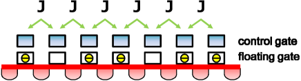
Here, we propose a QAM using the conventional NAND flash memory consisting of floating gate (FG) cells Masuoka ; Samsung ; Toshiba . NAND flash memory has a dominant share of the growing market for storage applications extending from mobile phones to data storage devices in data centers Takeuchi . The NAND flash memory has the advantages of high-density memory capacity and low production cost per bit with low power consumption and high-speed programming and erasing mechanisms. Data storage of personal computers is also transitioning from hard disk to flash memory. An FG cell corresponds to 1 bit for a single level cell type and bit for a multi-level type. Each FG is typically made of highly doped polysilicon and placed in the middle of a gate insulator of a transistor Brown ; Aritome . If there is no extra charge in an FG, the cell behaves like a normal transistor. In the programming or writing step, electrons are injected into the FG by applying voltage to the control gate. In the erasing step, electrons are ejected from the FG to the substrate by applying voltage to the back gate. The amount of the charge of FG determines the threshold voltage above which the current between the source and drain changes. In NAND flash memories, the FG cells are connected like a NAND gate. In general, the distance between the FGs is of the same order as the size of FG, resulting in high-density memory. For example, Sako et al. developed 64 Gbit NAND flash memory in 15 nm CMOS technology Toshiba , which is organized by a unit of 16KB bit-lines 128 word-lines. This means that the number of closely arrayed FG cells in a single unit is 16KB128 2MB. The integration and miniaturization of flash memory cells have progressed continuously and the current flash memories have stacked 3D structures using trapping layers Samsung2 ; Toshiba2 .
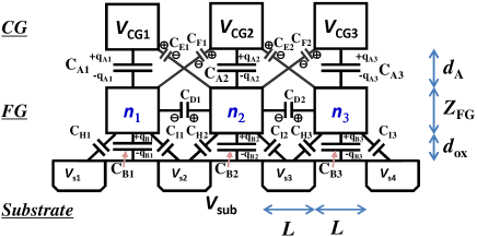
We theoretically prove that a two-dimensional (2D) FG array can be used as a QAM. The QAM proposed here has the structure shown in Fig.1. The FG cells are capacitively connected to each other, which is the same arrangement as that in a commercial flash memory. The fundamental idea is that we will be able to regard a small FG cell in the single-electron region as a charge qubit. Now the size of the FG NAND flash memory is 15 nm iedm2012 ; iedm2013 , and the size can shrink to beyond 7 nmTSMC7nm ; Samsung7nm ; IBM7nm . In the flash memory with 15 nm cell, single-electron effects can be observed at room temperature Nicosia . When the doping concentration of electrons is cm-3, the number of electrons in a volume of 151550 nm3 is about 1125 and countable. Once we can control the single-electron effects, we can realize a two-level system by using a crossover region between two different quantum states with different numbers of electrons, following such as Ref. Makhlin .
The distance between FG cells is of the same order as the size of FG cells in conventional NAND flash memories. Thus, the capacitive coupling cannot be neglected Lee . The changes of electrostatic potentials of neighboring cells affect the electronic static potentials of target FG cells. In regard to the conventional use of the memory cell, these capacitance couplings between FG cells are undesirable. In the conventional NAND flash memories, this effect is alleviated by computer software of various error-correcting codes. But, here we use this coupling as the interaction between quantized cells. We derive the Ising interaction term and the Zeeman term in Eq. (2) from a simple capacitance network model.
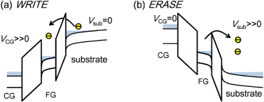
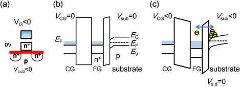
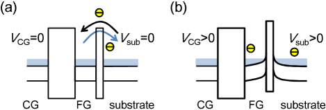
In the conventional usage of FG memory, the gate voltage is applied either positively or negatively corresponding to WRITE (programming data) and ERASE (erasing data) processes, respectively. Thus, in order to realize the tunneling between the FG cells and the substrate in both directions, both gate electrode and substrate have the same voltage whereas the voltage of FG should be low. By controlling the voltages, we realize the third term of Eq. (2).
This QAM has two major structural differences compared with conventional FG memories. The first major difference is that the tunnel barrier between FGs and substrate in the present proposal is thinner than that of the commercial FG array, in order to realize the bidirectional tunneling. The second major difference is that we do not use the air-gap between FG cells iedm2013 in order to increase the electrostatic coupling between FG cells.
Semiconductor devices consist of many different regions on the substrate. There are several doping concentrations with n-type and p-type semiconductors. The conventional FG devices are based on the silicon transistor with additional floating gates. Thus, there are several regions with different electrostatic potentials. It is necessary to investigate how the above-mentioned idea can be implemented in a realistic potential profile. Here, we use a technology computer aided design (TCAD) tool to check whether we can generate the desired potential profile of tunneling within an appropriate voltage region. Although this simulator does not include the single-electron effect and we provide results of coupling three cells, we can sketch a rough engineering drawing in a realistic situation.
The great advantage of using semiconductor devices instead of superconducting devices is that they are the smallest structures that humans can reliably integrate in Gbit order. Our proposed QAM will be able to be fabricated using a mask set and a product line that are almost same as those used for the conventional NAND flash memory. We believe that integration capabilities backed by mass-production technologies will eventually lead to quantum computers that are far more controllable than those available today. This QAM will be of far more benefit than QAMs without commercial antecedents in mass-productions, because the progress from fundamental science to a commercial product involves a huge cost and time.
This paper is organized as follows: In Sec. II, we briefly review an implementation of a QAM for a 2D qubit array. In Sec. III, we explain the basic idea of how to implement QAM into an FG array. In Sec. IV, we derive an Ising Hamiltonian from an FG array. In Sec. V, we present the results of TCAD simulation based on realistic FG sizes. In Sec. VI, we discuss the noise and decoherence problem of our QAM. In Sec. VII, we discuss the possibility of high-frequency operation. We close with a summary and conclusions in Sec. VIII. Additional information is presented in the Appendix.
II How to construct QAM in 2D NAND flash memory structure
The simpler the structure and mechanism, the greater is the reduction in variations among cells, and the more stable the operations become. Thus, in order to realize a reliable large-scale QAM, the structure and mechanism should be as simple as possible. For the simplest QAM, the coupling has a fixed value determined by its cell structure. The typical optimization problem with a fixed is the MAX-CUT problem MAXCUT ; Kahruman . The MAX-CUT problem is given as follows: Given a graph , with weights for all , the max-cut is a problem of finding such that the cut is the maximum. Introducing the variables: if , if . The max cut problem can be expressed as finding the minimum of the Ising model of under a constraint of for . The MAX-CUT problem MAXCUT ; Kahruman is applied to the noise reduction problem Yamaoka . On the other hand, in general, the values of the coupling are chosen depending on each optimization problem Lucas . For example, in the traveling salesman problem, s are taken as the distances between two cities Lucas . Thus, there is a trade-off between the range of application and the simplicity of device structure. Here, we consider a QAM whose coupling is determined by the capacitive coupling between two FG cells. Because the distances between FG cells are all the same, a fixed value of is provided in our system in its original condition. Note that this limitation can be resolved and arbitrary variable of can be realized by applying high-frequency electric fields as shown in Ref. Niskanen . Because we would like to present the fundamental proposal of QAM based on FG arrays, we will concentrate on our QAM for a conventional operation region of the fixed .
In addition, we consider a 2D planer FG array. In order to solve general problems in the QAM, all connections between two cells are required IonTrap . This means that the coupling should be formed in any two cells. A coherent Ising machine CIM ; Yamamoto can realize this situation by using optical systems. Because the connections between solid-state cells are fixed, it is not possible to directly connect two arbitrary cells in solid-state circuits with minimum distances. If we apply the methods proposed in Ref. Valiant ; Choi ; Lidar , we can implement connections between distant qubits. We can also use the advantage of conventional circuits, i.e., we can implement digital circuits for connecting distant FG cells similar to Ref. Yamaoka . In this case, there is no quantum coherence between digitally connected FG cells. Although the speed up is less than that of a fully quantum-connected QAM, it is still expected to operate in the partial quantum regions.
Let us think about using the lithography mask set of the conventional NAND flash memory of Ref. Toshiba . The ‘page’ in NAND flash memory corresponds to the number of the digital bits in the bit-line. Because Ref. Toshiba has 2 bits per cell, the number of connected FG cells in the direction is 128 and one block consists of 16KB 128=16384 2MB cells. These blocks are digitally connected and form the single plane of the memory. This means that the coupling s exists between nearest neighboring 2MB cells. Thus, ideally, 2MB FG charge qubits form an entangled state. By connecting the blocks digitally, we would be able to realize a quantum annealing machine like that of Ref. Yamaoka . Hereafter, we would like to prove that the 2D FG cell array realizes the Ising Hamiltonian with the fixed . The digital connection and concrete application to annealing problems are beyond the scope of this paper.
III Basic idea of QAM based on FG array
We would like to conceptually explain how to realize a QAM in the conventional FG structure.
III.1 Floating gate cell
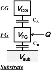
First, let us consider the single-electron effect in FG cells. The basic physics of the FG cell can be explained by the simple model of series of capacitance depicted in Fig. 2 given by Pavan
| (4) |
where is a charge stored in the FG. , and are potential energies of the control gate(CG), FG, and substrate, respectively. From Eq. (4), we have
| (5) |
This equation shows that the FG potential energy is determined by the charging energy of FG (1st term of the right side of the equation) and the controllability of CG and substrate. When the capacitance is sufficiently small, the change of the number of single electrons can be detected if is larger than the operation temperature . If we simply express , where , , and are the dielectric constant of a tunneling oxide SiO2, the area, and the thickness of the capacitor, and use the value of F/nm, nm2, and =3.5 nm, we have the voltage shift, =0.00721 eV =83.8 K, by the change of a single electron Nicosia . (The Boltzmann constant K/(eV) is used.) Thus, the single-electron effect will be detectable. Because the single-electron region can be used to construct a two-level system as Makhlin et al. Makhlin showed, the small size of the FG gate array allows construction of a two-level system, which is quantitatively discussed in the next section.
As in the field of FG memory, we define a coupling ratio defined by
| (6) |
as an indication of the degree of controllability of the gate electrode. We also assume that the capacitance is represented by a simple parallel plate capacitor such as
| (7) |
where and are the length and width of the FG cell, and are the thickness of tunneling oxides, and and are dielectric constants. Then, when and are given, is given by and is given by
| (8) |
III.2 Interaction between FG cells
In commercial 2D NAND flash memories Toshiba ; Samsung ; iedm2013 ; iedm2012 the distance between FG cells is of the same order as the size of the FG cells. Thus, the interference effects between FG cells are one of the major issues in NAND flash memories Lee . In order to reduce the interference between FG cells, the air-gap technologies are used iedm2013 , because the dielectric constant of air is smaller than that of the tunneling oxide such as SiO2 (whose dielectric constant is 3.8). However, here we use SiO2 between FG cells to increase the electrostatic coupling between FG cells.
III.3 Tunneling
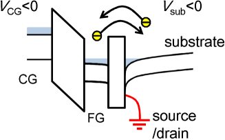
In the conventional FG memory, tunneling phenomenon of electrons is used for WRITE and ERASE processes of data by biasing the voltage between the gate and substrate electrodes. However, in the conventional WRITE and ERASE processes, electron flow is unidirectional as shown in Figs. 3(a) and (b). In the case of a QAM, electron tunneling should be bidirectional between the FG and substrate. Bidirectional tunneling occurs when we lower the potential of the interface between the FG and substrate. This situation will be realized by biasing the gate and substrate electrodes compared with the source and drain as shown in Fig.4.
In the conventional FG memory, the thickness of the tunneling oxide is about 7 nm to store charges for more than a couple of years when there is no bias on the gate and substrate. For the WRITE or ERASE process, a large bias of more than 10 V is applied to add or extract electrons from FGs. In this biasing process, because of the large applied bias, the tunneling potential changes and Fowler-Nordheim tunneling is realized Pavan . In order to realize bidirectional tunneling, we consider a case of thin tunneling oxide.
III.4 FG array
Figure 5 shows a schematic of a 2D FG cell array. The FG cells are coupled capacitively with each other in both word and bit directions. The source and drain are attached to the both ends of bit-lines. When we look at each bit-line, biases are applied to the source and drain as well as to the gate. Thus, the regions between FG cells in the bit-line are in electronically floating states. In order to switch on the tunneling of all FG cells at once, we will have to apply higher gate voltage to the cells far from the source and drain.

IV Derivation of QAM Hamiltonian from FG array
Here, we derive the Ising Hamiltonian from the FG array described in Fig. 1 by using a capacitance network model (Fig. 6). The charging energy is reduced to the 1st and 2nd term of Eq. (2). The last term of Eq. (2) is derived from tunneling of carriers between FGs and substrate. We assume that the FG cells are sufficiently small that the single-electron effects is observable. The Ising interaction is derived from the interference effect between cells Lee . This interference effect is the result of Coulomb interaction between the charges of neighboring FG cells. Usually this interference effect is an obstacle to the conventional flash memories. But here we can use it effectively for the cell-to-cell interaction.
IV.1 Ising interaction parts and Zeeman energy
Here, we derive the 1st and 2nd term of Eq.(2) by describing the FG cells using the capacitance network model described in Fig. 6.
IV.1.1 Analytical formation of Ising interaction parts and Zeeman energy
The charging energy of FG cells is expressed by
where , and . The number of charges in the -th FG is given by
| (10) |
where . The capacitances are defined by
| (11) | |||||
| (12) |
with and . For simplicity, from now on we formulate a case of three cells.
The charge distribution is obtained after minimizing the capacitance energy by using the method of Lagrange multipliers tana0 ; tana1 and given by
| (13) | |||||
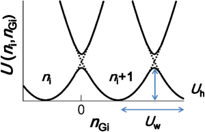
We consider a Coulomb blockade region where the number of electrons can be controlled such that we can define a quantum state by the number of electrons in -th FG as shown in Fig. 7. The superposition state is constituted by the coupling region of and , which is realized when the parabolic charging energy of state crosses that of state as discussed in Ref. Makhlin . The crossover point where the charging energy of electrons equals that of the electrons is given by
| (14) |
When we define an effective gate voltage given by
| (15) |
then, the crossover point is given by and the superposition state is constituted around . accounts for the effect of the gate voltage of the -th cell.
Thus, the charging energy term as a function of is transformed to
| (16) |
where
| (17) | |||||
| (18) | |||||
| (19) |
and
| (20) | |||||
| (21) | |||||
| (22) |
(Details of the definitions and derivations are noted in the Appendix). We can define a height of charging energy as the coefficient of in Eq.(17) and given by
| (23) |
is defined by a voltage difference of the parabolas for and . When we see as a function of the gate voltage , we obtain from two equations of and .
When the quantum computations, such as Grover’s algorithm Grover , are carried out, we have to maintain the electronic system in the range of its two-level system. For that purpose, we have to maintain the superposition state between and in the present setup, and we have to take care such that or states do not affect the target quantum operations, when we apply the gate and substrate bias beyond . In contrast, the purpose of the quantum annealing process is to finally obtain the state. Thus, as long as we can restore the point of , we can apply the gate and substrate bias beyond .
IV.1.2 Numerical estimation of charging part
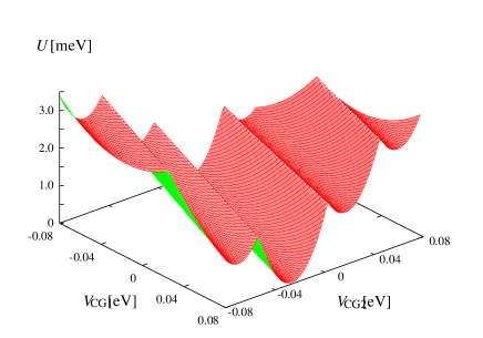
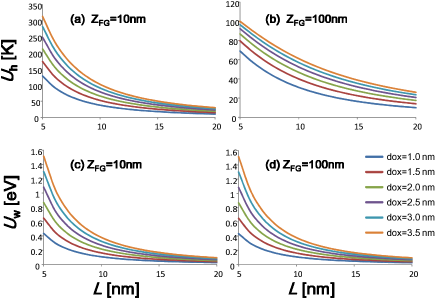
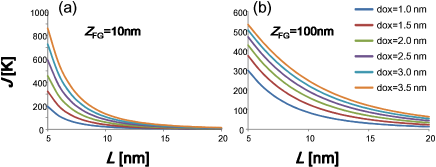
Figure 8 shows an example of the numerical calculation of the charging energy of three coupled FG cells for and nm with . In order to experimentally observe single-electron effects, the charging energy should be sufficiently large to be observed at the operation temperature. It is found that smaller is better for increasing charging effects. Each parabola has its own electronic state of a fixed . Where two parabolas cross, the charging energies of different numbers of electrons cross as shown in Eq. (14). Figure 9 shows and as functions of the size of FGs with various parameters of the thickness of the tunneling barrier . indicates a metric of charging energy, and therefore, is described as a unit of temperature in Fig. 9. indicates a metric of gate controllability, and therefore, is described as a unit of voltage in Fig. 9. From Figs. 9, it can be seen that a smaller FG is better for a larger charging energy as expected. It is also found that thicker is desirable. Comparison of Fig. 9(a) and Fig. 9(b) reveals that smaller height of FG is better for higher temperature operations.
Figure 10 shows , Eq. (19), as a function of the size of the FG. As the size becomes larger, the magnitude of becomes smaller. It can be also seen that the larger is better for larger . This is because the larger induces a larger area of Coulomb interactions with their neighboring FGs.
IV.2 Derivation of tunneling part
IV.2.1 Analytical formation of tunneling term
Here, we derive the tunneling term in Eq. (2) by using the WKB approximation as shown in Ref. Harrison . The tunneling term is expressed in the form of annihilation operators and given by
where is the potential height of the tunneling barrier, and are the effective masses of electrons in Si and tunneling barrier, respectively (is an electron mass in vacuum). and c are annihilation operators of both sides of the tunneling barrier. is a wave vector at a Fermi energy. nm is the Bohr radius and eV is the Rydberg constant. is a volume of tunneling electrons, and , are the numbers of electrons of the two sides of the tunneling barrier, respectively, which participate in the tunneling event, given by
| (25) |
This tunneling term is a function of the gate voltage through the shift of Fermi energy such as , and is calculated by the FG doping concentration for which we use 1020 cm-3. When increases, the effective tunneling barrier is lowered and the tunneling rate increases (switch on). Conversely, when decreases, the effective tunneling barrier becomes larger, and the tunneling is switched off. Thus, the tunneling can be switched on or off by controlling the gate and substrate bias.
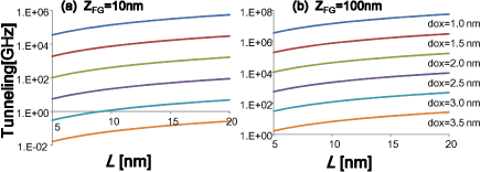
IV.2.2 Numerical estimation of tunneling term
Figure 11 shows a result of the numerical calculations of the tunneling term as a function of the FG sizes when and are changed. It can be seen that the tunneling rate increases as and increase. These are opposite trends to and in Fig. 9, and show that the increasing tunneling rate makes the saving of electrons difficult. Tables 1 and 2 show typical results from Figs. 9-11 as a summary of the basic calculations mentioned above.
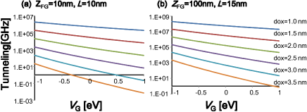
Figure 12 shows the amplitude of the tunneling term as a function of . It is seen that, when we change in the range of V, we can change the tunneling rate in the range of 104. For example, for nm and nm in Fig. 12(b), the tunneling term for =0 is approximately 26.4 Hz and can be neglected. That for =-1 V corresponds to a case that an electron tunneling is expected to occur by approximately 2.2kHz.
IV.2.3 Normally-off and normally-on
So far, we have considered a QAM in which tunneling is switched on when external biases are applied. Thus, these devices can be called “normally-off” devices. On the other hand, as becomes thinner, the tunneling frequency becomes larger and larger and the tunneling is always on even for . For example in Fig. 12(a), the tunneling term for nm of nm is 17.1 THz, and in Fig. 12(b), the tunneling term for nm is 1717 THz. For these cases, we can switch off the tunneling by applying positive electric voltages. Thus, we call these devices “normally-on” devices. Compared with normally-off devices, the power consumption of the normally-on devices is considered to be larger. Thus, we mainly consider the normally-off devices and discuss the normally-on devices briefly in the Appendix.
TABLE 1. Examples of the result of the analytical calculations for nm and 10 nm. Size [K] [K] Tunnel [GHz] [eV] =5 nm 596.0 249.7 5.61 1.08 =10 nm 85.8 80.4 22.5 0.27 =15 nm 23.5 39.5 50.5 0.12
TABLE 2. Examples of the result of the analytical calculations for nm and nm. Size [K] [K] Tunnel [GHz] [eV] =5 nm 534.4 100.1 1.65 1.52 =10 nm 251.0 61.5 6.61 0.38 =15 nm 124.0 39.3 14.9 0.17
V Results of TCAD simulations
In general, FG memories consist of many different regions with different doping concentrations and doping types. Different regions have different work functions without bias. Typically, a p-type substrate, n-type source/drain and an n-type FG are employed where the doping concentration of the FG is higher than that in the substrate. Figure 13(a) shows the typical doping pattern. Figures 13(b) and (c) show the band structures depending on a bias voltage.
Here, we would like to show the results of the conventional TCAD simulation in our targeted parameter regions. We calculated the device characteristics of the three FG array of Fig. 13(a) by using our in-house TCAD simulator. This simulator was developed for conventional semiconductor devices, and cannot include the single-electron effect. The number of the coupled cells is limited by our calculation resources. Here we do not calculate (Eq.(17)) nor (Eq.(19)), because capacitances change depending on applied biases as a result of the change of depletion layers. Elaborate estimation will be required. Accordingly, the crossover point of in Fig. 7 should be estimated in the near future.
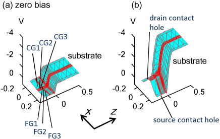
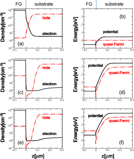
In order to generate electrons at the surface of the substrate (Fig. 13(b) and (c)), is required Grove . Figure 14 shows the bird’s eye views of the electronic potentials of zero bias (Fig. 14(a)) and the case of V and V (Fig. 14(b)). Figure 15 shows the calculated electron and hole densities, potential energies and quasi-Fermi energies. It is realized that the electron density is larger than the hole density at the substrate interface. It can be also seen that Figs. 15 (c) and (d) are similar to Figs. 15(e) and (f), respectively. This means that the case of , and is an extension of the case of when . The quasi-Fermi energy and potential energy of the FGs in Fig. 15(f) become higher than those of Fig. 15(d) while the bottom of the quasi-Fermi energy at the substrate surface does not significantly change. This is the expected result in Fig. 4.
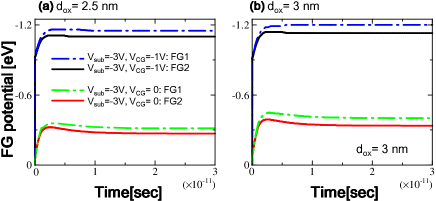
We also calculated a time dependent FG potential as shown in Fig. 16 to see the dynamic behavior of tunneling. We apply finite voltages on the gate and substrate at sec, starting from zero bias state. It can be seen that the time scale of the change of the potentials is of the order of sec. Thus, tunneling event is very fast as estimated in the previous sections.
VI Noise and decoherence
Here, we discuss the noise and decoherence problems in the QAM based on an FG array. In the conventional FG array, the thickness of the tunneling oxide is of the order of 7 nm to store the charge in the FG for many years. In the present setups, we apply a thinner tunneling oxide ( nm ) to control switching on and off the tunneling. Thus, natural leakage of charges occurs more often than in the case of the conventional FG memory. Therefore, after the QAM process, the results should be quickly transferred to a conventional memory block.
The unexpected trap sites are ones of the problems of NAND flash memories Paolucchi1 ; Paolucchi2 ; Aritome2 . These will become more serious when we use an FG array as a qubit system. However, the physical properties of the traps persist on each cell as shown in Ref. Kim ; Chen . Once we check the trap distributions and their properties and store that information to conventional memory, we could apply appropriate voltages depending on each FG cell and improve the QAM performance.
Next, let us estimate the coherence time by taking into account the electron-phonon interactions, following the discussion in Ref. tana0 . We assume that the acoustic phonon in the tunneling material of SiO2 is the principal origin of decoherence and apply the standard spin-boson theory Legget . According to Leggett et al. Legget , the complete information about the effect of the environment is encapsulated by the spectral function . In the present case, the two-state system is formed through the tunneling of SiO2 and it has two types of spectral function given by Garcia ; Wurger
| (26) |
The first term shows a superohmic dissipation and corresponds to an underdamped coherent oscillation, whose damping rate at is given by tana0
| (27) |
where is the renormalized tunneling frequency , and given by
| (28) |
When we use eV, m/s, kg/m-3, and with K, we have , and thus this term can be neglected. The second term of Eq. (26) expresses an ohmic dissipation. The parameter of the ohmic dissipation is given by . Then is given by
| (29) | |||||
| (30) |
where and . When we estimate the coherence time from the exponential part of such as , we have msec for K and msec for K, respectively. Therefore, the increase of the tunneling excites more phonons, and a low tunneling rate is desirable. However, tunneling that is too slow induces many noises Paolucchi1 ; Paolucchi2 ; Aritome2 . Thus, there will be an optimal point for the tunneling rate, depending on each system.
VII Discussion
In Ref. tana0 ; tana1 , we have proposed a charge-qubit system NEC ; transmon based on coupled quantum dots (CQDs) Stockklauser . When we regard FGs as quantum dots (QDs), the previous CQD proposal is different from the present proposal in that there are additional FGs stacked on the first FG layer tana2 . Although additional fabrication processes are required for the CQD system, the structure of the CQD system can be manufactured by the same set of photo masks as that in the present proposal. Because the electron moves in the close-coupled QDs in the previous proposal, its coherence time is considered to be longer than that of the present proposal. Besides the fact that the present proposal is more close to the conventional flash memory, the advantage of the present proposal is that the electron tunneling is directly changed by the external electrodes. In contrast, the tunneling barrier of the CQD system is fixed, and qubit states are mainly controlled in the rotating frame by applying high-frequency electric field.
We have to readout the final state after the annealing process. At the readout stage, the number of electrons in the FG should be detected by applying gate voltage and switching on current between the source and drain. As in the conventional FG array, the applied voltage of the reading out is smaller than that of the ‘switching-on’ process. The readout process should not change the number of electrons in the FG array. The thickness of the tunneling oxide of the normally-off type is greater than that of the normally-on type (as discussed in the Appendix). Thus, it is considered that the normally-off type is more easily constructed than the normally-on type. In any event, detailed optimizations of the structure and operation voltages are subjects for future work.
VIII Conclusion
We have shown that the conventional FG memory structure can be used as the quantum annealing machine. It is assumed that the FG is sufficiently small for the appearance of the single-electron effect. The electrostatic Coulomb interaction between FG cells is the origin of the Ising interaction. The tunneling between the FG and substrate is brought about by applying voltages to both the CG and substrate, while the source/drain voltage is set to zero. Using TCAD simulation, we have shown an example of the device characteristics under possible bias conditions. Optimization of many parameters is a subject for future work.
Acknowledgements.
We thank A. Nishiyama, M. Koyama, S. Yasuda, H. Goto, D. Matsushita, K. Matsuzawa and T. Ishihara for discussions.Appendix A Detailed derivation process of the charging energy
Here, we show additional information for the derivation process of Eq.(16). The parameters in Eq.(13) in the text are given by
| (31) |
where . Following Ref .Makhlin , we consider the region around
| (32) |
This is the region where the charging energy of electrons equals that of the electrons, and the and states constitute a superposition state. We use the effective gate voltage given by
| (33) |
(). For this region, we can approximate the following equation
| (34) |
where , are Pauli matrix and unit matrix, respectively, based on system. Thus, we obtain Eq.(16) and
| (35) | |||||
Appendix B Normally-on and normally-off
In the main text, we consider a case in which tunneling occurs only when the gate and substrate biases are applied. These devices can be called ”normally-off” devices. In this section, we briefly discuss a “normally-on” device in which tunneling is switched off only when the gate and substrate bias are applied.
Figure 17 shows an example of the normally-on set up. The electron tunneling always occurs between the FG and the substrate without bias as shown in Fig. 17(a). The effective thickness of the effective tunneling barrier is changed by the change of the potential of the FG and substrate. If we prepare a p-type substrate like that of the conventional NAND flash memory, the current from the substrate to the source and drain flows when the tunneling is switched off (Fig.17(b)). This is because the source and drain are n-type semiconductors. Thus, in the normally-on type QAM, there are always some current flows in the cell. Detailed calculations are subjects for future work.
References
- (1) T. Kadowaki and H. Nishimori, Quantum annealing in the transverse Ising model, Phys. Rev. E 58, 5355 (1998).
- (2) A. B. Finnila, M. A. Gomez, C. Sebenik, C. Stenson, and J. D. Doll, Quantum Annealing: A New Method for Minimizing Multidimensional Functions, Chem. Phys. Lett. 219, 343 (1994).
- (3) M. W. Johnson et al.,Quantum annealing with manufactured spins, Nature 473, 194 (2011).
- (4) T. Lanting et al., Entanglement in a Quantum Annealing Processor Phys. Rev. X 4, 021041 (2014).
- (5) A. Lucas, Ising formulations of many NP problems, Front. Phys. 2, 5 (2014).
- (6) M. Yamaoka, C. Yoshimura, M. Hayashi, T. Okuyama, H. Aoki, and H. Mizuno, 20k-spin Ising Chip for Combinational Optimization Problem with CMOS Annealing, 2015 IEEE Int. Solid State Circuits Conference (ISSCC), 1 (2015).
- (7) T.D Ladd, F. Jelezko, R. Laflamme, Y. Nakamura, C. Monroe, and J.L. ÓBrien, Quantum computers, Nature 464, 45 (2010).
- (8) M. Veldhorst et al., A two- qubit logic gate in silicon, Nature 526, 410 (2015).
- (9) F. Masuoka, M. Momodomi, Y. Iwata, and R. Shirota, New ultra high density EPROM and Flash EEPROM with NAND structure cell, 1987 Int. Electron Devices Meeting (IEDM), 552 (1987).
- (10) M. Sako et al., A Low-Power 64Gb MLC NAND-Flash Memory in 15 nm CMOS Technology, 2015 IEEE Int. Solid State Circuits Conference (ISSCC), 7.1 (2015).
- (11) D. Kang et al., 256Gb 3b/Cell V-NAND Flash Memory with 48 Stacked WL Layers, 2016 IEEE Int. Solid State Circuits Conference (ISSCC), 7.1 (2016).
- (12) K. Takeuchi, T. Hatanaka, and S Tanakamaru, Highly reliable, high speed and low power NAND flash memory-based Solid State Drivers (SSDs), IEICE Electronics Press, 9, 779 (2012).
- (13) Nonvolatile Semiconductor Memory Technology: A Comprehensive Guide to Understanding and Using NVSM Devices, edited by W.D. Brown and Joe Brewer, (publisher Wiley-IEEE Press, New York, 1997).
- (14) S. Aritome, Advanced Flash Memory Technology and Trends for File Storage Application, 2000 IEEE Int. Electron Devices Meeting (IEDM), 763 (2000).
- (15) C. Kim et al., A 512Gb 3b/cell 64-Stacked WL 3D V-NAND Flash Memory, 2017 IEEE Int. Solid State Circuits Conference (ISSCC), 11.4 (2017).
- (16) R. Yamashita et al., A 512Gb 3b/Cell Flash Memory on 64-Word-Line-Layer BiCS Technology, 2017 IEEE Int. Solid State Circuits Conference (ISSCC), 11.1 (2017).
- (17) J. Seo et al., Highly Reliable M1X MLC NAND Flash Memory Cell with Novel Active Air-gap and p+ Poly Process Integration Technologies, 2013 IEEE Int. Electron Devices Meeting (IEDM), 76 (2013).
- (18) A. Goda and K. Para, Scaling Directions for 2D and 3D NAND Cells, 2012 IEEE Int. Electron Devices Meeting (IEDM), 13 (2012).
- (19) J. Chang et al., A 7nm 256Mb SRAM in High-K Metal-Gate FinFET Technology with Write-Assist Circuitry for Low-VMIN Applications, 2017 IEEE Int. Solid State Circuits Conference (ISSCC), 12.1 (2017).
- (20) T. Song et al., A 7nm FinFET SRAM Macro Using EUV Lithography for Peripheral Repair Analysis, 2017 IEEE Int. Solid State Circuits Conference (ISSCC), 12.2 (2017).
- (21) T. Nogami, et al., Comparison of Key Fine-Line BEOL Metallization Schemes for Beyond 7 nm Node, 2017 IEEE Symp. VLSI Tech. 148 (2017).
- (22) G. Nicosia et al., A single-electron analysis of NAND flash memory programming, IEEE Int. Electron Devices Meeting (IEDM), 378 (2015).
- (23) Y. Makhlin, G. Schön, and A. Shnirman, Quantum-state engineering with Josephson-junction devices, Rev. Mod. Phys. 73, 357 (2001).
- (24) J. D. Lee, S. H. Hur, and J.D. Choi, Effects of floating-gate interference on NAND flash memory cell operation, IEEE Electron Device Letters 23, 264 (2002).
- (25) S. Sousa, Y. Haxhimusa, and W.G. Kropatsch, Estimation of Distribution Algorithm for the Max-Cut Problem, Int. Workshop on Graph-Based Representations in Pattern Recognition GbRPR 2013: Graph-Based Representations in Pattern Recognition, 244 (2013).
- (26) S. Kahruman et al., On Greedy Construction Heuristics for the MAX-CUT problem, Int. J. of Computational Science and Engineering, 3, 211 (2007).
- (27) A. O. Niskanen, Y. Nakamura, and J.S. Tsai, Tunable coupling scheme for flux qubits at the optimal point, Phys. Rev. B 73, 094506 (2006).
- (28) T. Gra, D. Ravento, B. Juliá-Díaz, C. Gogolin, and M. Lewenstein, Quantum annealing for the number-partitioning problem using a tunable spin glass of ions, Nat. Commun. 7 11524 (2016).
- (29) T. Inagaki, et al., A coherent Ising machine for 2000-node optimization problems, Science 354 603 (2016).
- (30) P.L. McMahon et al., A fully programmable 100-spin coherent Ising machine with all-to-all connections, Science 354 614 (2016).
- (31) L.G. Valiant, Universality Considerations in VLSI Circuits, IEEE Trans. Comput. C30(2), 135 (1981).
- (32) V. Choi, ”Minor-embedding in adiabatic quantum computation: II. Minor-universal graph design”, Quantum Information Processing 10 343 (2011).
- (33) S. Boixo, T. Albash, F.M. Spedalieri, N. Chancellor, and D.A. Lidar, Experimental signature of programmable quantum annealing, Nat. Commun. 4, 3067 (2013).
- (34) P. Pavan, L. Larcher, and A. Marmiroli, “Floating Gate Devices: Operation and Compact Modeling”, (Kluwer, Boston, 2004).
- (35) T. Tanamoto, Quantum gates by coupled asymmetric quantum dots and controlled-NOT-gate operation, Phys. Rev. A 61, 022305 (2000).
- (36) T. Tanamoto, One-and two-dimensional N-qubit systems in capacitively coupled quantum dots, Phys. Rev. A 64, 062306 (2001).
- (37) L.K. Grover, Quantum Mechanics Helps in Searching for a Needle in a Haystack, Phys. Rev. Lett., 78, 325 (1997).
- (38) W. A. Harrison, Tunneling from an Independent-Particle Point of View, Phys. Rev. 123, 85 (1961).
- (39) A. S. Grove, “Physics and Technology of Semiconductor Devices”, (Wiley, New York, 1967).
- (40) G. M. Paolucci, C. Monzio Compagnoni, C. Miccoli, A. S. Spinelli, A. L. Lacaita, and A. Visconti, Revisiting charge trapping/detrapping in flash memories from a discrete and statistical standpoint—Part I: VT instabilities, IEEE Trans. Electron Devices, 61. 2802 (2014).
- (41) G. M. Paolucci, C. M. Compagnoni, C. Miccoli, A. S. Spinelli, A. L. Lacaita, and A. Visconti, Revisiting charge trapping/detrapping in Flash memories from a discrete and statistical standpoint—Part II: Onfield operation and distributed-cycling effects, IEEE Trans. Electron Devices, 61, 2811 (2014).
- (42) S. Aritome, T. Takahashi, K. Mizoguchi, and K. Takeuchi, RTN Impact on Data-Retention Failure/Recovery in Scaled (1Ynm) TLC NAND Flash Memories, 2017 IEEE Int. Reliability Physics Symposium (IRPS), PM.13, (2017).
- (43) M. S. Kim, D. I. Moon, S. K. Yoo, and S. H. Lee, Investigation of Physically Unclonable Functions Using Flash Memory for Integrated Circuit, IEEE Trans. Nanotech 14, 384 (2015).
- (44) J. Chen, T. Tanamoto, H. Noguchi, and Y. Mitani, Further investigations on traps stabilities in random telegraph signal noise and the application to a novel concept physical unclonable function (PUF) with robust reliabilities, 2015 IEEE Symp. VLSI Tech. 40 (2015).
- (45) A.J. Leggett, S. Chakravarty, A.T. Dorsey, and M.P. A. Fisher, Dynamics of the dissipative two-state system, A. Garg, and W. Zwerger, Rev. Mod. Phys. 59, 1 (1987).
- (46) A. J. Garcćia and J. Fernández, Phonon-dressing effects on two-level systems in amorphous solids and their influenceon the low-temperature specific heat, Phys. Rev. B 55, 5546 (1997).
- (47) A. Würger, Ohmic Dissipation of Tunneling in Dielectric Glasses at Low Temperature, Europhys. Lett. 28, 597 (1994).
- (48) T. Yamamoto Y. A. Pashkin, O. Astafiev, Y. Nakamura and J. S. Tsai Demonstration of conditional gate operation using superconducting charge qubits, Nature 425, 941 (2003).
- (49) J. Koch, T. M. Yu, J. Gambetta, A. A. Houck, D. I. Schuster, J. Majer, A. Blais, M. H. Devoret, S. M. Girvin, and R. J. Schoelkopf Charge-insensitive qubit design derived from the Cooper pair box Phys. Rev. A 76, 042319 (2007).
- (50) A. Stockklauser, P. Scarlino, J. V. Koski, S. Gasparinetti, C. K. Andersen, C. Reichl, W. Wegscheider, T. Ihn, K. Ensslin, and A. Wallraff, Strong Coupling Cavity QED with Gate-Defined Double Quantum Dots Enabled by a High Impedance Resonator, Phys. Rev. X 7, 011030 (2017).
- (51) T. Tanamoto and K. Muraoka, Numerical approach for retention characteristics of double floating-gate memories, Appl. Phys. Lett. 96, 022105 (2010).