Correlated electronic states at domain walls of a Mott-charge-density-wave insulator 1T-TaS2
Domain walls in interacting electronic systems can have distinct localized states, which often govern physical properties and may lead to unprecedented functionalities and novel devices. However, electronic states within domain walls themselves have not been clearly identified and understood for strongly correlated electron systems. Here, we resolve the electronic states localized on domain walls in a Mott-charge-density-wave(CDW) insulator 1T-TaS2 using scanning tunneling spectroscopy. We establish that the domain wall state decomposes into two nonconducting states located at the center of domain walls and edges of domains. Theoretical calculations reveal their atomistic origin as the local reconstruction of domain walls under the strong influence of electron correlation. Our results introduce a concept for the domain wall electronic property, the wall’s own internal degrees of freedom, which is potentially related to the controllability of domain wall electronic properties.
Conductive domain walls and their functionalities catalan2012domain have been reported in multiferroic insulators seidel2009conduction ; meier2012anisotropic ; oh2015experimental , magnetic insulators yamaji2014metallic ; ma2015mobile , Mott insulators kivelson1998elctronic , and layered CDW materials sipos2008mott ; yu2015gate ; joe2014emergence ; li2015controlling . CDW with periodic modulations of charge/lattice at low temperature and their domain walls are widely observed in metallic layered transition metal dichalcogenides wilson1975charge . Among them, 1-TaS2 shows a series of CDW transitions coupled to substantial electron-electron interaction. Especially, a metal-insulator transition occurs below 190 K through a transition from a nearly commensurate to a commensurate CDW state disalvo1975effects . The insulating ground state is realized by electron correlation on narrow electron bands formed by the commensurate CDW lattice fazekas1979electrical . Recent experimental results have demonstrated that the correlated insulating ground state can be transformed into various quasi-metallic and superconducting CDW states by external and internal control parameters, such as pressure sipos2008mott , optical (electrical) excitation stojchevska2014ultrafast ; yoshida2015memristive ; tsen2015structure ; cho2016nanoscale ; ma2016ametallic ; vaskivskyi2016fast , and chemical doping xu2010superconducting ; ang2012real ; ang2013superconductivity . These conductivity switchings are intrinsically very fast, which may make possible novel ultrafast devices based on correlated electrons.
In the metallic excited states, CDW domain walls are common objects and considered as the origin of the metallic property. They have been suggested as highly conducting channels themselves sipos2008mott ; stojchevska2014ultrafast ; tsen2015structure and/or to screen electron correlation within Mott-CDW domains xu2010superconducting . Moreover, the emerging superconductivity out of the Mott-CDW insulating phase has been considered being directly related to conducting domain walls sipos2008mott ; yu2015gate ; liu2016nature . However, despite such long discussion, the electronic states of domain walls have not yet been clarified spectroscopically. Here, we show that the domain walls in 1-TaS2 have two well-confined and non-metallic in-gap states above Fermi level () using scanning tunneling microscopy and spectroscopy (STM and STS). They are located on the domain wall center and edges of neighboring domains, respectively. The theoretical calculations strongly suggest the substantial correlation effect in forming spatially decomposed and non-metallic domain wall states.
Results
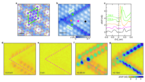
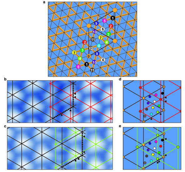
Domain walls in the insulating CDW state. Figure 1a shows a typical STM image of the commensurate Mott-CDW state in 1-TaS2 at 4.3 K. The unit layer of 1-TaS2 consists of a Ta layer sandwiched by two S layers with each Ta atom coordinated octahedrally by S atoms. Unpaired 5 electrons of Ta form a half-filled metallic band which is unstable against the CDW formation driven by strong electron-phonon coupling. Ta atoms undergo a reconstruction into a so called David-star unit cell which is composed of 13 Ta atoms; the 12 outer atoms pair up and shift toward the central one brouwer1980the , where a unpaired 5 electron is left over fazekas1979electrical ; smith1985band . In the commensurate CDW phase, David-star unit cells (green lines in Fig. 1a) exhibit a regular triangular lattice with a period of 12.1 and its STM image is dominated by protrusions representing unpaired electrons of central Ta atoms kim1994observation . The on-site Coulomb repulsion drives these unpaired electrons into a Mott insulating state, which form otherwise a narrow metallic band. In this way, the insulating state is driven by a cooperative interplay between the CDW and the electron-electron interaction cho2015interplay .
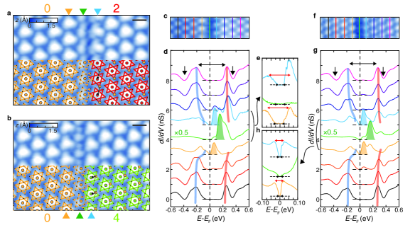
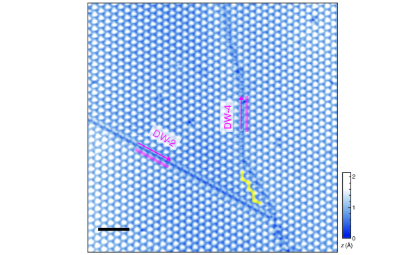
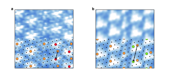
In spite of the clear commensurability and the long range order of the undoped low temperature phase, there exist one-dimensional intrinsic defects, domain walls, across which the phase of CDW is abruptly shifted (see Fig. 1b and Supplementary Figure 1). Since there can be 13 atoms within a CDW unit cell, 12 anti-phase domain wall configurations are possible as indexed in Fig. 1a ma2016ametallic . The configuration of a domain wall can be easily identified by the phase shift (black arrows in Fig. 2a, b) of CDW protrusions of neighboring domains (see Supplementary Figure 2). Only few cases among 12 configurations are observed including the most popular ones shown in Fig. 2, probably because of the energetics and/or kinetics of the domain wall formation ma2016ametallic ; wu1990direct . The present work covers two most popular and straight domain walls [indexed as the 2nd (upper) and the 4th (lower) one following the atomic indices of Fig. 1a] which were found to be stable within the experimental time scale. We mainly focus on the 2nd domain wall which is the majority species cho2016nanoscale ; ma2016ametallic .
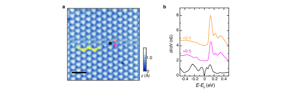
Localized in-gap states of the domain wall and edges. Electronic states localized on domain walls are revealed by acquiring STS spectra around domain walls with a high spatial resolution. The previous STS work showed only enhanced spectral weight around the band gap region without observing any distinct electronic states ma2016ametallic . In the present work, for example, STS spectra were measured at each pixel of the STM image containing two domain walls of different but most popular types (Fig. 1b). Within the Mott gap region of -0.1 +0.2 eV around , one can observe two pronounced localized electronic states. A strong spectral feature appears along the center of domain walls in the empty state at +0.15 eV (two green curves in Figs. 1c and 1g) and another one also in the empty state at +0.08 eV (a orange curve in Figs. 1c and 1f) but slightly away from the center of domain walls. The latter is localized along the edge of neighboring domains and a similar but weak feature also appears in the filled state at -0.05 eV (Fig. 1d). Note that we do not observe any distinct spectral weight at which is essential for domain-wall-originated metallicity or superconductivity (Fig. 1e). The present result is consistent with our recent work for nearly commensurate domain wall networks cho2016nanoscale . The localized in-gap state above were also observed on zigzag domain walls (see Supplementary Figure 3).
The maps at the energies of the in-gap states show charge modulations along domain walls and edges. Their periodicities are the same as that of the David-star reconstruction. These domain wall and edge states exhibit specific phase relations determined by the phase difference between neighboring domains across the domain wall (see Supplementary Figure 2 and 4). This implies that the domain wall reconstruction is strongly influenced by the periodic potential imposed by the CDW reconstruction in neighboring domains barja2016charge .
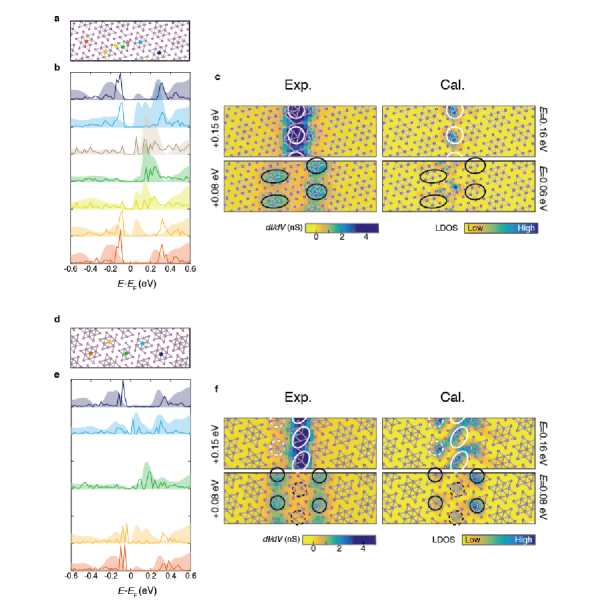
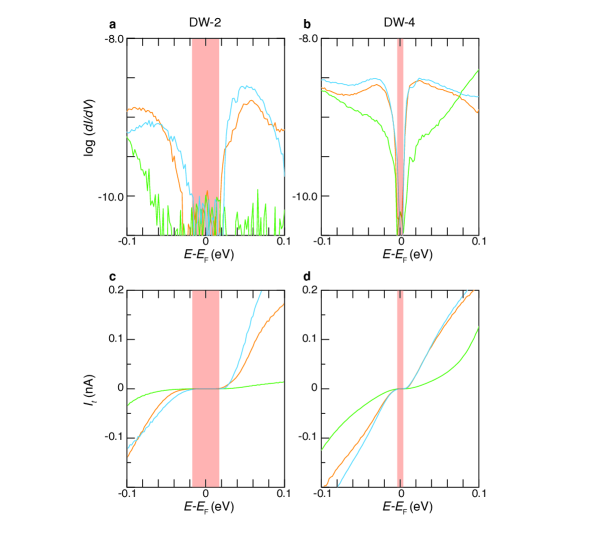
Gapped nature of domain walls and their localized electronic states become more clear in a closer look of point-by-point STS spectra. Figures 2a and 2b show well resolved STM images of the 2nd and 4th domain walls, which are the same types as those of Fig. 1b. Within domain walls, David-star CDW units cannot be formed completely and the incomplete David-stars reconstruct into pairs of small and large protrusions along domain walls. This will be discussed in more detail below. A series of spectra across domain walls are shown in Figs. 2d and 2g. Away from domain walls, the curves reproduce the energy gap of the Mott-CDW state; two Hubbard states construct a Mott gap of 0.440.02 eV. The subband splittings (single-headed black arrows in Fig. 2d, 2g) are footprints of the formation of CDW and the David-star reconstruction smith1985band ; cho2015interplay . Upon approaching the domain wall, CDW protrusions and STS spectra do not show a noticeable spatial variation except for a tiny band bending until they reach the last CDW unit cells of domains, which we call domain edges. As discussed above, at domain edges in both sides of the domain wall, an in-gap state emerges at +0.07 eV. Then, at the domain wall center, the Hubbard states are replaced by a strong spectral feature of +0.15 eV. Note that the domain wall itself is not metallic at all as also shown in the spatial maps at (Fig. 1d). While the edges of domains have higher spectral weight near , the band gap on the domain edge can be unambiguously defined by the edge of the lower Hubbard band and the new spectral feature above . Their peak-to-peak splitting are 120 meV and 50 meV on the 2nd and 4th domain wall, respectively (red double headed arrows in the Fig. 2e and 2h). Due to thermal and instrumental broadenings, these spectral features leave decaying intensities toward , which obscure the band gap. However, our higher resolution STS measurements (see Methods) clearly show the zero conductance region at (see Fig. 2e, 2h, and Supplementary Figure 5), which makes the existence of the band gap unambiguous.
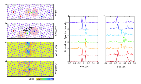
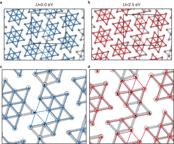
Correlation dependent domain wall and edge reconstructions. In order to elucidate the origin of the domain wall and edge states, first principles calculations were performed. We used a domain supercell in a monolayer 1-TaS2 in which a single domain is composed of five columns of David-stars. Each domain is shifted to construct domain wall of the 2nd type between neighboring domains. The equilibrium structure after a full relaxation of atomic positions is shown in Fig. 3a. Here we use the usual density functional theory framework without putting any extra electron correlation, which substantially underestimates the Mott-CDW band gap at (Fig. 3e) darancet2014three . The two overlapped David-star columns in the domain wall region simply split into two symmetric rows of incomplete David-stars with 12 Ta atoms on each. This produces a unique electronic state on the domain wall at the energy of conduction band minimum (arrows in Fig. 3e). This domain wall structure and its electronic state deviate qualitatively from what were observed. We then include the extra electron correlation effect with a finite value within the GGA+ scheme. The value is tuned up to 2.5 eV in order to properly reproduce the experimentally observed Mott gap of the CDW domain (Fig. 3f). With the enhanced electron correlation, the domain wall reconstruction drastically changes; it becomes much narrower with 11 Ta atoms, which split longitudinally into centered hexagons and linear tetramers (see Supplementary Figure 6). The atomic lattice of the domain wall is resolved in our high resolution STM topography while small lattice distortions due to the reconstruction within are hardly detected ma2016ametallic (see Supplementary Figure 7). However, strong charge modulations relevant with the atomic reconstruction are shown clearly in our STM and STS results. The hexagon on the domain wall center exhibits an electronic state at a slightly lower energy than the upper Hubbard band (a green arrow in Fig. 3f). The other states at a lower energy closer to (a blue and orange arrow in Fig. 3f) emerges at the edges of hexagons and extends to neighboring David-stars units, that is, to domain edges (Fig. 3f). The 4th domain wall has also the spatially decomposed in-gap states and a smaller gap feature are reproduced in our calculations eV (see Supplementary Figure 4). This result strongly suggests the crucial role of electron correlation in the formation of the domain wall electronic state.
We note that there are still discrepancies between the calculation and the measurement, especially in the spatial distribution of edge states (see Supplementary Figure 4). The maxima of calculated edge states (Fig. 3d) are located closer to the narrow domain wall than those observed while the tendency to spread toward edges of domains is consistent. We suspect that this discrepancy may be related to the interlayer coupling discussed in the previous studies cho2016nanoscale ; ma2016ametallic ; darancet2014three ; ritschel2015orbital , which is not included at all in our calculations.
Discussion
The electronic state(s) within the band gap observed here is in line with localized states suggested in sharp phase kinks of order parameters in charge or spin ordered insulators seidel2009conduction ; ma2015mobile ; salafranca2010jahn ; cheon2015chiral . Our STM and STS results disclose that the domain wall is not a metallic channel developed by the suppression of the CDW order, which have been assumed by many previous studies sipos2008mott ; stojchevska2014ultrafast ; tsen2015structure ; liu2016nature .On the other hand, a few other studies suggested that free carriers from domain wall electronic states screen the electron correlation in neighboring CDW domains xu2010superconducting . This idea was critically tested in the present work with a clearly negative answer. The domain wall junctions shown in Fig. 1b is a good testbed for the screening effect since the CDW domain in between the two domain walls would have an increasingly larger effect of the screening, if any, when approaching closer to the junction point. However, our STS data do not show any substantial change of electronic states from that of the Mott-CDW gap structure as approaching the junction (Fig. 1c), except for the domain wall and edge states (the yellow spectrum in Fig. 1c). This result clearly rules out the screening scenario to explain the metallicity of the textured CDW states. Of course, the metallic state can be driven by developing a random disorder potential in Mott insulators and decreasing the CDW lateral or vertical ordering cho2016nanoscale . However, the single isolated and straight domain wall as discussed here is not related to such a global disorder to melt the correlation gap lahoud2014emergence ; chiesa2014emergence .
In summary, we discover distinct electronic states of domain walls of a symmetry-broken correlated insulator for the first time. The domain walls of the Mott-CDW phase of 1-TaS2 have well localized non-metallic in-gap states along the center of domain walls and the edges of neighboring domains. Not only the lack of free carriers but also the lack of any substantial screening or doping effects by domain walls are disclosed unambiguously. These results request to rewrite most of the current scenarios on the metallic and superconducting phases emerging from this correlated insulator. The origin of the split non-metallic domain wall states are clearly understood as due to the reconstruction within domain walls composed of multiple atoms and electrons under the substantial influence of electron correlation. That is, the internal structural and electronic degrees of freedom within domain walls are indicated to be very important. The internal structural degree of freedom of domain walls were recently noticed for one cheon2015chiral and two dimensional barja2016charge systems, but to the best of our knowledge, the substantial electron correlation effect within a domain wall has not been observed before. These internal degrees of freedom might be exploited to provide controllability of domain wall electronic properties for the functionalization of complex materials with domain walls.
Methods
Experiments.
The STM and STS measurements have been carried out with a commercial STM (SPECS) at 4.3 K. Pt-Ir wires were used for STM tips. All STM images were acquired with the constant current mode with bias voltage () applied to the sample. The standard lock-in technique with voltage modulation =10 mV and frequency =1 kHz has been adapted for acquiring spectra. The high resolution spectra were obtained with =2 mV. A single crystal of 1-TaS2 were prepared by iodine vapor transport method, as described in Ref. 18. The samples were cleaved at room temperature and quickly transferred to the pre-cooled STM head.
Theoretical Calculations.
Our calculations were carried out using density functional theory (DFT) with the projector augmented wave method, Perdew-Burke-Ernzerhof (PBE) exchange and correlation functional and GGA+ as implemented in the Vienna simulation package (VASP). To avoid interactions between the supercell, about 10 Å vacuum is inserted in vertical direction. The plane wave cut-off energy is set to 260.0 eV and the Monkhorst-Pack -point mesh is . All the atoms are relaxed until forces on the atoms are less than 0.02 eV/Å.
Acknowledgments
This work was supported by the Institute for Basic Science (Grant No. IBS-R014-D1). LW and SWC are partially supported by the Max Planck POSTECH/KOREA Research Initiative Program (Grant No. 2011-0031558) through NRF of Korea funded by MEST. SWC is also supported by the Gordon and Betty Moore Foundations EPiQS Initiative through Grant GBMF4413 to the Rutgers Center for Emergent Materials.
Author contributions
DC and HWY conceived the research idea and plan. DC and JL performed the STM / STS measurements. LW and SWC grew the single crystals. SHL and GG conducted the DFT calculations. DC and HWY prepared the manuscript with the comments of all other authors.
References
-
References
- (1) Catalan, G., Seidel, J., Ramesh, R., & Scott, J. F. Domain wall nanoelectronics. Rev. Mod. Phys. 84, 119-156 (2012).
- (2) Seidel, J., et al. Conduction at domain walls in oxide multiferroics. Nat. Mater. 8, 229-234 (2009).
- (3) Meier, D., et al. Anisotropic conductance at improper ferroelectric domain walls. Nat. Mater. 11, 284-288 (2012).
- (4) Oh, Y. S., et al. Experimental demonstration of hybrid improper ferroelectricity and the presence of abundant charged walls in (Ca,Sr)3 Ti2O7 crystals. Nat. Mater. 14, 407-413 (2015).
- (5) Yamaji, Y. & Imada, M. Metallic interface emerging at magnetic domain wall of antiferromagnetic insulator: Fate of extinct Weyl electrons. Phys. Rev. X 4 021035 (2014).
- (6) Ma, E. Y. et al. Mobile metallic domain walls in an all-in-all-out magnetic insulator. Science 350, 538-541 (2015).
- (7) Kivelson, S. A., Fradkin, E., & Emery, V. J. Electronic liquid-crystal phases of a doped Mott insulator. Nature 393, 550-553 (1998).
- (8) Sipos, B. et al. From Mott state to superconductivity in 1T-TaS2. Nat. Mater. 7, 960-965 (2008).
- (9) Yu, Y. et al. Gate-tunable phase transitions in thin flakes of 1T-TaS2. Nat. Nanotech. 10, 270-276 (2015).
- (10) Joe, Y. I. et al. Emergence of charge density wave domain walls above the superconducting dome in 1T-TiSe2. Nat. Phys. 10, 421-425 (2014).
- (11) Li, L. J. et al. Controlling many-body states by the electric-field effect in a two-dimensional material. Nature 529, 185-189 (2015).
- (12) Wilson, J. A., Di Salvo, F. J. & Mahajan, S. Charge-density waves and superlattices in the metallic layered transition metal dichalcogenides. Adv. Phys. 24, 117-201 (1975).
- (13) Di Salvo, F. J., Wilson, J. A., Bagley, B. G., & Waszczak, J. V. Effects of doping on charge-density waves in layer compounds. Phys. Rev. B 12, 2220-2235 (1975).
- (14) Fazekas, P. & Tosatti, E. Electrical structural and magnetic properties of pure and doped 1T-TaS2. Philos. Mag. B 39, 229-244 (1979).
- (15) Stojchevska, L. et al. Ultrafast switching to a stable hidden quantum state in an electronic crystal. Science 344, 177-180 (2014).
- (16) Yoshida, M. et al. Memristive phase switching in two-dimensional 1T-TaS2 crystals. Sci. Adv. 9, e1500606 (2015).
- (17) Tsen, A. W. et al. Structure and control of charge density waves in two-dimensional 1T-TaS2. Proc. Natl. Acad. Sci. U. S. A. 112, 15054-15059 (2015).
- (18) Cho, D. et al. Nanoscale manipulation of the Mott insulating state coupled to charge order in 1T-TaS2. Nat. Commun. 7, 10453 (2016).
- (19) Ma, L. et al. A metallic mosaic phase and the origin of Mott insulating state in 1T-TaS2. Nat. Commun. 7, 10956 (2016).
- (20) Vaskivskyi, I. et al. Fast electronic resistance switching involving hidden charge density wave states. Nat. Commun. 7, 11442 (2016).
- (21) Xu, P. et al. Superconducting phase in the layered dichalcogenide 1T-TaS2 upon inhibition of the metal-insulator transition. Phys. Rev. B 81, 172503 (2010).
- (22) Ang, R. et al. Real-space coexistence of the melted Mott state and superconductivity in Fe-substituted 1T-TaS2. Phys. Rev. Lett. 109, 176403 (2012).
- (23) Ang, R. et al. Superconductivity and bandwidth-controlled Mott metal-insulator transition in 1T-TaS2-xSex. Phys. Rev. B 88, 115145 (2013).
- (24) Liu, Y. et al. Nature of charge density waves and superconductivity in 1T-TaSe2-xTex. Phys. Rev. B 94, 045131 (2016).
- (25) Brouwer, R. & Jellinek, F. The low-temperature superstructures of 1T-TaS2 and 1H-TaSe2. Phys. B+C 99, 51-55 (1980).
- (26) Smith, N. V., Kevan, S. D. & Di Salvo, F. J. Band structures of the layer compounds 1T-TaS2 and 1H-TaSe2 in the presence of commensurate charge-density waves. J. Phys. C 18, 3175-3189 (1985).
- (27) Kim, J.-J., Yamaguchi, W., Hasegawa, T. & Kitazawa, K. Oservation of Mott localization gap using low temperature scanning tunneling spectroscopy in commensurate 1T-TaS2. Phys. Rev. Lett. 73, 2103-2106 (1994).
- (28) Cho, D. et al. Interplay of electron-electron and electron-phonon interactions in the low-temperature phase of 1T-TaS2. Phys. Rev. B 92, 085132 (2015).
- (29) Wu, X. L. & Lieber, C. M. Direct observation of growth and melting of the hexagonal-domain charge-density-wave phase in 1T-TaS2 by scanning tunneling microscopy. Phys. Rev. Lett. 64, 1150-1154 (1990).
- (30) Barja. S. et al. Charge density wave order in 1D mirror twin boundaries of single-layer MoSe2. Nat. Phys. 12, 751-756 (2016).
- (31) Darancet, P., Millis, A. J. & Marianetti, C. A. Three-dimensional metallic and two-dimensional insulating behavior in octahedral tantalum dichalcogenides. Phys. Rev. B 90, 045134 (2014).
- (32) Ritschel, T. et al. Orbital textures and charge density waves in transition metal dichalcogenides. Nat. Phys. 11, 328-331 (2015).
- (33) Salafranca, J., Yu, R., & Dagotto, E. Conducting Jahn-Teller domain walls in undoped manganites. Phys. Rev. B, 81, 245122 (2010).
- (34) Cheon, S., Kim, T. H., Lee, S. H. & Yeom, H. W. Chiral solitons in a coupled double Peierls chain. Science 350, 182-185 (2015).
- (35) Lahoud, E. et al. Emergence of a novel pseudogap metallic state in a disordered 2D Mott insulator. Phys. Rev. Lett. 112, 206402 (2014).
- (36) Chiesa, S., Chakraborty, P. B., Pickett, W. E., & Scalettar, R. T. Disorder-induced stabilization of the pseudogap in strongly correlated systems. Phys. Rev. Lett. 101, 086401 (2008).