Quantum dots with split enhancement gate tunnel barrier control
Abstract
We introduce a silicon metal-oxide-semiconductor quantum dot architecture based on a single polysilicon gate stack. The elementary structure consists of two enhancement gates separated spatially by a gap, one gate forming a reservoir and the other a quantum dot. We demonstrate, in three devices based on two different versions of this elementary structure, that a wide range of tunnel rates is attainable while maintaining single-electron occupation. A characteristic change in slope of the charge transitions as a function of the reservoir gate voltage, attributed to screening from charges in the reservoir, is observed in all devices, and is expected to play a role in the sizable tuning orthogonality of the split enhancement gate structure. The all-silicon process is expected to minimize strain gradients from electrode thermal mismatch, while the single gate layer should avoid issues related to overlayers (e.g., additional dielectric charge noise) and help improve yield. Finally, reservoir gate control of the tunnel barrier has implications for initialization, manipulation and readout schemes in multi-quantum dot architectures.
pacs:
Silicon (Si) quantum dots (QDs) are strong contenders for the realization of spin qubits Loss and DiVincenzo (1998); Zwanenburg et al. (2013). Silicon germanium heterostructure (Si/SiGe) platforms with integrated micromagnets Pioro-Ladrière et al. (2007) have produced the highest performance qubits Wu et al. (2014); Takeda et al. (2016); Kawakami et al. (2016), with fidelities over 99.9%Yoneda et al. (2018), while metal-oxide-semiconductor (MOS) platforms have also achieved fault tolerant fidelities Veldhorst et al. (2014).
Most of the high performance systems mentioned above are enhancement mode devices comprising at least two layers of control gates. The overlapping gates ensure strong confinement and the highest electrostatic control over regions surrounding the QDs. These current multi-stack devices have therefore achieved excellent tunability, thanks in part to an independant control of reservoirs, dots and tunnel barriers through respectively dedicated gates. On the other hand, single-layer enhancement mode devices are being explored for ease of fabrication and potentially higher yield, in both Si/SiGe and MOS systems Lu et al. (2016); Studenikin et al. (2018); Jock et al. (2018); Harvey-Collard et al. (2018, 2017). In particular, all-silicon MOS single-layer devices are expected to avoid thermal mismatch and additional dielectric charge noise from overlayers Thorbeck and Zimmerman (2015); Zimmerman et al. (2014). These single-layer devices generally use a single gate to form a source-dot-drain channel, relying on constrictions and lateral depletion gates to shape the confinement potential Lu et al. (2016); Tracy et al. (2013). Reservoir filling, dot charge occupation and tunnel rates are therefore controlled differently than in multi-gate stack architectures. Various architectures and methods of tunnel barrier control impact tunability differently, and understanding those differences will influence choices of multi-QDs initialization, manipulation and readout schemes, including automatic tuning procedures Baart et al. (2016); Van Diepen et al. (2018), as well as reproducibility, versatility and scalability of devices Frees et al. (2018).
Here we explore a single gate stack structure featuring a split gate for dot and reservoir formation. The tunnel barrier is simply formed by the gap between the dot and reservoir gates. We investigate, in all-silicon MOS devices based on this elementary structure, how tunnel barrier control can be achieved by modulation of the reservoir gate voltage. The operation principle is studied in two variations of the layout, emphasizing some intrinsic effects brought by the use of a reservoir gate for tunnel control, in contrast with the more frequent method of control using a dedicated barrier gate directly on top of the barrier. We also define a control orthogonality metric with significance for tunability and versatility of quantum dot devices and use it to compare a split gate QD device to a multi-stack device from the literature. Finally, we conclude by examining single-electron regime characteristics and valley splitting tuning in the split gate devices.
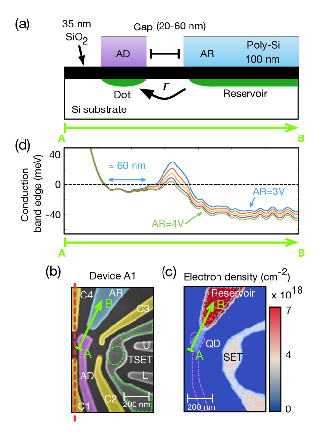
The elementary single-gate stack structure we explore consists of a quantum dot enhancement gate, AD, and a reservoir enhancement gate, AR, separated by a gap, as shown in Fig. 1(a). We refer to this base unit of design as the split enhancement gate structure. Devices are fabricated using the Sandia National Laboratories MOS quantum dot process Tracy et al. (2009); Singh et al. (2016), which is described in detail in the Supplementary Material. The gate stack consists of a 10 000 -cm n-type silicon float zone substrate, a 35 nm gate oxide and a degenerately As-doped 100 nm thick polysilicon gate (shown in Fig. 1(a)). The polysilicon nanostructure is defined by a single electron-beam lithography and dry etching step. The gate oxide properties have been characterized in Hall bars fabricated on the same starting gate stack as the nanostructures. Peak mobility, percolation density Tracy et al. (2009); Borselli et al. (2011a), scattering charge density Das Sarma and Hwang (2013); Tracy et al. (2009), interface roughness and interface correlation length Mazzoni et al. (1999) were extracted for the wafers used for each of the devices and are described in the Supplementary Material.
In this study, we look at two different layouts of split enhancement gate devices. We examine a single-lead layout (devices A1 and A2), where a single reservoir is connected to a dot, and a double-lead layout (device B), where the dot is connected in series to reservoirs to enable transport measurements, in addition to charge sensing. Devices A1 and A2 present the same layout, with only differences in scale and spacing (see Table I in the Supplementary Material). For all devices, measurements are performed using a proximal SET as a charge sensor with standard lock-in or RF reflectometry techniquesMüller et al. (2012). Details on the measurements and a list of all voltages employed are given in the Supplementary Material.
To illustrate the split enhancement gate tunnel barrier structure and its operation, we have performed Thomas-Fermi numerical simulations Gao et al. (2013) of device A1, as shown in Fig. 1(b), using the corresponding MOS structure and operating gate voltages as input parameters. Figure 1(c) shows the simulated electron density at the Si/ interface when the device is experimentally set in a 20 electrons regime. As expected, a reservoir is formed under gate AR, and a quantum dot under the tip of gate AD, separated by the tunnel barrier region. Some form of tunnel barrier control using the reservoir gate voltage, , is suggested by variations of the potential along the dot-reservoir axis (Fig. 1(d)). Indeed, as a function of , the tunnel barrier potential height and width are modified, while the QD conduction band edge stays fairly constant relative to the Fermi level of the reservoir, indicating some form of tuning orthogonality between charge occupation of the QD and tunnel rate to the reservoir (similar quantities are evoqued in Ref. Frees et al. (2018)). A sufficient tuning orthogonality would allow simultaneously for a wide range of tunnel rates and the ability to regularly tune these devices to the single electron regime. We therefore investigate this characteristic for a QD based on a split enhancement gate structure employing the reservoir gate as a knob Shirkhorshidian et al. .
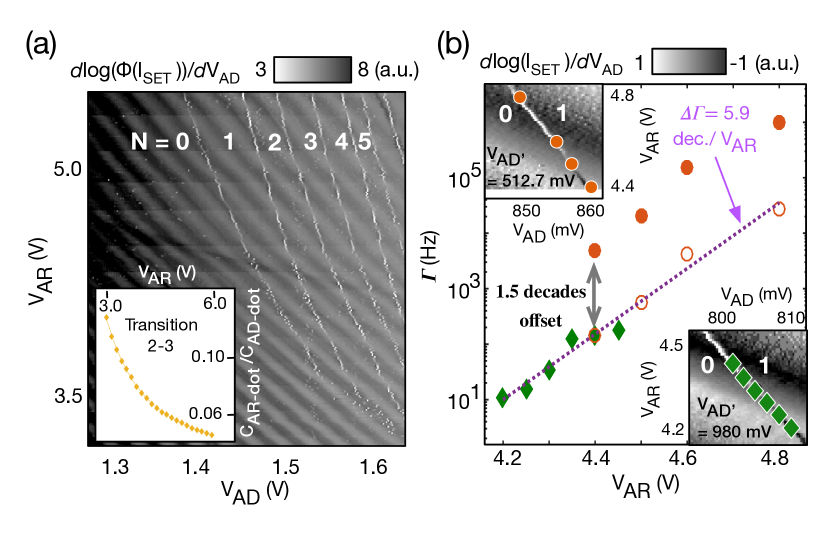
Figure 2(a) shows how the QD occupancy can be tuned down to the single electron regime in device A2 (similar to device A1 except for scale, see Supplementary Material). The single electron occupation was confirmed with spin filling from magnetospectroscopy, and yields an 8 meV charging energy for the last electron. The effect of on the tunnel rate is qualitatively visible from the charge transitions, which go from a “smooth” appearance at high , when is high compared to the measurement rate, to a speckled appearance at low , when is of the order of the measurement rate or lower Thalakulam et al. (2010).
We observe a gradual decrease of the AR gate capacitance to the dot, , as the reservoir fills up with electrons, as shown in the inset of Fig. 2(a) (assuming , the capacitance of the AD gate to the dot, stays constant) . The capacitance ratio is extracted from the slope of the transition in the stability diagram Grabert et al. (1993). A similar dependence of the capacitance ratio is also observed in numerical simulations, but the agreement is only qualitative, due in part to the limitations of the semi-classical simulation. We attribute this visible curvature in the dot transitions to a screening effect of the reservoir gate potential, induced by the accumulated charges in the reservoir. This specific effect therefore seems to be caused by the use of an enhancement gate connected to a ohmic contact as a tuning knob.
Device A1 also exhibits a comparable behavior as a function of the AR and AD gate voltages (see Supplementary Material). We measured the dot-reservoir tunnel rate as a function of the voltage on gate AR for device A1, along the charge transition, as was compensated with to preserve the charge state, as shown in Fig. 2(b). Two data sets (diamond and filled circles) were taken at different voltages on a surrounding gate, . The 467 mV difference results in a 1.5 decades global offset in tunnel rates. We subtract this offset (hollow circles) to extract a single exponential dependence of with Borselli et al. (2015); MacLean et al. (2007).
From the slope of the exponential fit, we extract a gate response of decades/, defined as the variation in dot-reservoir tunnel rate induced by a change of 1 V on gate AR, when compensated by gate AD to keep the dot chemical potential fixed. More useful for comparison between devices is when we remove the device geometry specific capacitance by converting to change in chemical potential, . We define the following metric:
| (1) |
where is the change in tunnel rate induced by the change in voltage on AR (and compensated by AD), is the change in chemical potential caused by gate AR (equal to the chemical potential compensated by gate AD), and we call the tuning orthogonality. For device A1, the above analysis leads to decade/meV, using the gate lever arm meV/mV (from meV/mV). We note that the chemical potential of the QD does not actually shift for a given tunnel rate variation here, since there is a second gate compensating the chemical potential shift from the first. Therefore, care must be taken in interpreting this ratio: it does not represent the effect of a single gate on the tunnel rate, but rather the interplay of two gates acting in opposite direction on the two quantities, with unequal contributions.
Taken individually, more positive voltages on gates AD and AR would both tend to decrease the barrier height and width, as one would expect and as shown in the conduction band edge simulations of Fig.1(d). But if one wants to keep the dot occupation fixed, and shift from high to low tunnel rates, gates AD and AR have to be swept in opposite directions. Our measurements indicate that in this case the lever of gate AR on the tunnel barrier still overcomes the opposite effect of gate AD. Furthermore, we speculate that the screening effect from charges under AR contributes to this efficiency, as it reduces the lever of gate AR on the dot occupation, but on the tunnel barrier, such that less compensation on AD is necessary to maintain charge occupation than if no screening effect was present.
The quantity can be estimated for other designs in the literature, for any pair of gates 1 and 2 used to tune the tunnel rate and compensate for changes in the dot occupation, respectively. For comparison, we estimate decades/meV for the case of a dedicated barrier gate BG compensated by the dot accumulation gate AD equivalent in a Si/SiGe device Zajac et al. (2015). This indicates a tuning orthogonality that can reach the same order of magnitude as dedicated barrier gate devices in multi-stack architectures. The single-layer split enhancement gate layout could therefore provide a wide operation range Ciorga et al. (2000) for single-electron QD devices. Details on the calculations as well as assumptions leading to the metric and its limitations are provided in the Supplementary material.
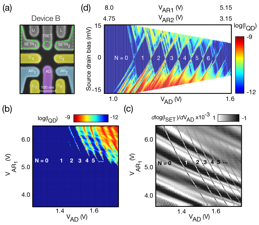
The double-lead layout also supports transport down to the last electron and exhibits a typical split enhancement gate behavior. Figure 3(a) shows device B, where transport is through a QD under gate AD with source and drain reservoirs under gates and . A mirrored structure can be operated as a SET charge sensor, correlating the transport transitions (Fig. 3(b)) with charge sensed measurements (Fig. 3(c)).
In Fig. 3(b), the tunnel rate ranges from the life-time broadened regime at high , corresponding to a 3 GHz tunnel rate Zajac et al. (2015); De Franceschi et al. (2001) to slower than can be detected by the charge sensor, 8 Hz. The slight curvature in the dot and SET transitions of Fig. 3(d) is ascribed to a similar screening effect as in the single lead devices, although it is not as pronounced. This demonstrates that two neighboring barriers in series can be tuned relatively orthogonally (i.e., crosstalk is not a prohibitive issue), and that the split enhancement gate concept can be applied in several layouts.
In Fig.3(d), and are adjusted simultaneously to symmetrize the tunnel barriers on the source and drain side of the QD, giving rise to Coulomb diamonds Kouwenhoven et al. (1997). The notable difference in voltage ranges applied on and is attributed mainly to asymmetry in the voltages applied on the neighboring gates on the left and right side of the device, although small variations in width of the dot-reservoir gap could also contribute to the difference. The precise effect of the dot-reservoir gap width on the tuning orthogonality and general efficiency remains to be studied in detail.
The addition energy of the last electron and the first orbital energy are extracted from the Coulomb diamonds of Fig. 3(d), yielding approximately meV and meV, respectively. A classical capacitance between the QD and the AD gate of 2.9 aF is estimated (e.g., with meV the voltage applied on gate AD to go from the charge transition to the transition in Fig. 3(b)). The classical capacitance can be associated with a circular 2D QD below the gate and is used to estimate a QD radius of 30 nm, using for the and neglecting small errors due to the electron offset from the interface and depletion of the polysilicon. The orbital energy also provides an estimate of QD size. Following Ref. Zajac et al. (2015), we can extract an effective length of a confining 2D box () and using 3 meV, we obtain a similar dot size, 25 nm, using . These estimated dot sizes and energies are similar to the ones obtained in multi-stack accumulation mode quantum dot devices Zajac et al. (2015); Angus et al. (2007).
Finally, an investigation of the spin filling and singlet-triplet energy splitting in our silicon QDs using magnetospectroscopy Borselli et al. (2011b); Lim et al. (2011); Zajac et al. (2015) indicates that the valley splitting is linearly tunable with the vertical electric field (eVm/MV in the double-lead device) and is tunable over a range of eV (see the Supplementary Material for details).
In conclusion, we explored a split enhancement gate architecture implemented in single-lead and double-lead layouts of polysilicon MOS QD devices. The single-electron regime was reliably achieved in three different devices. Using the reservoir enhancement gate to modulate the tunnel rate and compensating with the dot enhancement gate, we found a tuning orthogonality decade/meV in one of the single-lead devices. We argue that the notable tuning orthogonality, which is comparable to what can be achieved in devices with a dedicated barrier gate in multi-stack architectures, is boosted by the screening effect arising from the use of an enhancement gate as a tuning knob. In addition, a strongly confined quantum dot with charging energies up to 11 meV and orbital energy of 3 meV was observed in the device with smallest features, corresponding to a nm radius QD. Linear tunability of the QD’s valley splitting was also observed up to 250 eV.
Supplementary Material
Section I of the Supplementary Material provides details on the samples fabrication. Section II describes experimental details and devices characteristics. Section III presents a discussion on the tuning orthogonality metric, and Section IV is dedicated to the study of the valley splitting tuning in the split enhancement gate devices.
Acknowledgements.
We gratefully recognize conversations with J. K. Gamble about early split gate designs, and J. Dominguez for supporting preparation of the devices. We acknowledge technical support from M. Lacerte, R. Labrecque, and M. Lapointe-Major, and helpful discussions with J. Camirand Lemyre, L. Schreiber and J. Klos. This work was supported by the Natural Sciences and Engineering Research Council of Canada (NSERC) and the Canada Foundation for Innovation (CFI). This research was undertaken thanks in part to funding from the Canada First Research Excellence Fund. This work was performed, in part, at the Center for Integrated Nanotechnologies, an Office of Science User Facility operated for the U.S. Department of Energy (DOE) Office of Science. Sandia National Laboratories is a multimission laboratory managed and operated by National Technology and Engineering Solutions of Sandia, LLC, a wholly owned subsidiary of Honeywell International, Inc., for the U.S. Department of Energy’s National Nuclear Security Administration under contract DE-NA0003525. This paper describes objective technical results and analysis. Any subjective views or opinions that might be expressed in the paper do not necessarily represent the views of the U.S. Department of Energy or the United States Government.References
- Loss and DiVincenzo (1998) D. Loss and D. P. DiVincenzo, Physical Review A 57, 120 (1998).
- Zwanenburg et al. (2013) F. A. Zwanenburg, A. S. Dzurak, A. Morello, M. Y. Simmons, L. C. L. Hollenberg, G. Klimeck, S. Rogge, S. N. Coppersmith, and M. A. Eriksson, Reviews of Modern Physics 85, 961 (2013).
- Pioro-Ladrière et al. (2007) M. Pioro-Ladrière, Y. Tokura, T. Obata, T. Kubo, and S. Tarucha, Applied Physics Letters 90, 024105 (2007).
- Wu et al. (2014) X. Wu, D. R. Ward, J. R. Prance, D. Kim, J. K. Gamble, R. T. Mohr, Z. Shi, D. E. Savage, M. G. Lagally, M. Friesen, S. N. Coppersmith, and M. A. Eriksson, (2014), 10.1073/pnas.1412230111, arXiv:1403.0019 .
- Takeda et al. (2016) K. Takeda, J. Kamioka, T. Otsuka, J. Yoneda, T. Nakajima, M. R. Delbecq, S. Amaha, G. Allison, T. Kodera, S. Oda, and S. Tarucha, Science Advances 2, e1600694 (2016), arXiv:1602.07833 .
- Kawakami et al. (2016) E. Kawakami, T. Jullien, P. Scarlino, D. R. Ward, D. E. Savage, M. G. Lagally, V. V. Dobrovitski, M. Friesen, S. N. Coppersmith, M. A. Eriksson, and L. M. K. Vandersypen, Proceedings of the National Academy of Science of the United States , 1 (2016), arXiv:1602.08334 .
- Yoneda et al. (2018) J. Yoneda, K. Takeda, T. Otsuka, T. Nakajima, M. R. Delbecq, G. Allison, T. Honda, T. Kodera, S. Oda, Y. Hoshi, N. Usami, K. M. Itoh, and S. Tarucha, Nature Nanotechnology 13, 102 (2018), arXiv:1708.01454 .
- Veldhorst et al. (2014) M. Veldhorst, J. C. C. Hwang, C. H. Yang, a. W. Leenstra, B. de Ronde, J. P. Dehollain, J. T. Muhonen, F. E. Hudson, K. M. Itoh, A. Morello, and a. S. Dzurak, Nature nanotechnology , 1 (2014).
- Lu et al. (2016) T. M. Lu, J. K. Gamble, R. P. Muller, E. Nielsen, D. Bethke, G. A. Ten Eyck, T. Pluym, J. R. Wendt, J. Dominguez, M. P. Lilly, M. S. Carroll, and M. C. Wanke, Applied Physics Letters 109, 10 (2016), arXiv:arXiv:1608.08107v1 .
- Studenikin et al. (2018) S. A. Studenikin, L. Gaudreau, K. Kataoka, D. G. Austing, and A. S. Sachrajda, Applied Physics Letters 112, 233101 (2018).
- Jock et al. (2018) R. M. Jock, N. T. Jacobson, P. Harvey-Collard, A. M. Mounce, V. Srinivasa, D. R. Ward, J. Anderson, R. Manginell, J. R. Wendt, M. Rudolph, T. Pluym, J. K. Gamble, A. D. Baczewski, W. M. Witzel, and M. S. Carroll, Nature Communications 9, 1 (2018), arXiv:1707.04357 .
- Harvey-Collard et al. (2018) P. Harvey-Collard, B. D’Anjou, M. Rudolph, N. Tobias Jacobson, J. Dominguez, G. A. Eyck, J. R. Wendt, T. Pluym, M. P. Lilly, W. A. Coish, M. Pioro-Ladrière, and M. S. Carroll, Physical Review X 8, 1 (2018), arXiv:1703.02651 .
- Harvey-Collard et al. (2017) P. Harvey-Collard, N. T. Jacobson, M. Rudolph, J. Dominguez, G. A. Ten Eyck, J. R. Wendt, T. Pluym, J. K. Gamble, M. P. Lilly, M. Pioro-Ladrière, and M. S. Carroll, Nature Communications 8, 1 (2017), arXiv:1512.01606 .
- Thorbeck and Zimmerman (2015) T. Thorbeck and N. M. Zimmerman, AIP Advances 5 (2015), 10.1063/1.4928320, arXiv:1409.3549 .
- Zimmerman et al. (2014) N. M. Zimmerman, C.-H. Yang, N. Shyan Lai, W. Han Lim, and A. S. Dzurak, Nanotechnology 25, 405201 (2014), arXiv:1406.7475 .
- Tracy et al. (2013) L. A. Tracy, T. M. Lu, N. C. Bishop, G. A. Ten Eyck, T. Pluym, J. R. Wendt, M. P. Lilly, and M. S. Carroll, Applied Physics Letters 103 (2013), 10.1063/1.4824128.
- Baart et al. (2016) T. A. Baart, P. T. Eendebak, C. Reichl, W. Wegscheider, and L. M. Vandersypen, Applied Physics Letters 108 (2016), 10.1063/1.4952624, arXiv:1603.02274 .
- Van Diepen et al. (2018) C. J. Van Diepen, P. T. Eendebak, B. T. Buijtendorp, U. Mukhopadhyay, T. Fujita, C. Reichl, W. Wegscheider, and L. M. Vandersypen, Applied Physics Letters 113 (2018), 10.1063/1.5031034, arXiv:arXiv:1803.10352v1 .
- Frees et al. (2018) A. Frees, J. K. Gamble, D. R. Ward, R. Blume-Kohout, M. A. Eriksson, M. Friesen, and S. N. Coppersmith, , 1 (2018), arXiv:1806.04318 .
- Tracy et al. (2009) L. A. Tracy, E. H. Hwang, K. Eng, G. A. Ten Eyck, E. P. Nordberg, K. Childs, M. S. Carroll, M. P. Lilly, and S. Das Sarma, Physical Review B - Condensed Matter and Materials Physics 79, 1 (2009), arXiv:arXiv:0811.1394v2 .
- Singh et al. (2016) M. Singh, J. L. Pacheco, D. Perry, E. Garratt, G. Ten Eyck, N. C. Bishop, J. R. Wendt, R. P. Manginell, J. Dominguez, T. Pluym, D. R. Luhman, E. Bielejec, M. P. Lilly, and M. S. Carroll, Applied Physics Letters 108 (2016), 10.1063/1.4940421.
- Borselli et al. (2011a) M. G. Borselli, K. Eng, E. T. Croke, B. M. Maune, B. Huang, R. S. Ross, A. A. Kiselev, P. W. Deelman, I. Alvarado-Rodriguez, A. E. Schmitz, M. Sokolich, K. S. Holabird, T. M. Hazard, M. F. Gyure, and A. T. Hunter, Applied Physics Letters 99, 063109 (2011a).
- Das Sarma and Hwang (2013) S. Das Sarma and E. H. Hwang, Physical Review B - Condensed Matter and Materials Physics 88, 1 (2013), arXiv:arXiv:1304.4668v1 .
- Mazzoni et al. (1999) G. Mazzoni, A. L. Lacaita, L. M. Perron, and A. Pirovano, IEEE Transactions on Electron Devices 46, 1423 (1999).
- Müller et al. (2012) T. Müller, J. Güttinger, D. Bischoff, S. Hellmüller, K. Ensslin, and T. Ihn, Applied Physics Letters 101 (2012), 10.1063/1.4733613, arXiv:arXiv:1204.4216v1 .
- Gao et al. (2013) X. Gao, E. Nielsen, R. P. Muller, R. W. Young, a. G. Salinger, N. C. Bishop, M. P. Lilly, and M. S. Carroll, Journal of Applied Physics 114, 164302 (2013).
- (27) A. Shirkhorshidian, J. K. Gamble, L. Maurer, S. M. Carr, J. Dominguez, T. Eyck, J. R. Wendt, E. Nielsen, N. T. Jacobson, M. P. Lilly, and M. S. Carroll, , 1arXiv:arXiv:1705.01183v2 .
- Gustavsson et al. (2009) S. Gustavsson, R. Leturcq, M. Studer, I. Shorubalko, T. Ihn, K. Ensslin, D. C. Driscoll, and a. C. Gossard, Surface Science Reports 64, 191 (2009), arXiv:0905.4675 .
- Elzerman et al. (2004) J. M. Elzerman, R. Hanson, L. H. Willems van Beveren, L. M. K. Vandersypen, and L. P. Kouwenhoven, Applied Physics Letters 84, 4617 (2004).
- Thalakulam et al. (2010) M. Thalakulam, C. B. Simmons, B. M. Rosemeyer, D. E. Savage, M. G. Lagally, M. Friesen, S. N. Coppersmith, and M. a. Eriksson, Applied Physics Letters 96, 183104 (2010).
- Grabert et al. (1993) H. Grabert, M. H. Devoret, and M. Kastner, Physics Today 46, 62 (1993).
- Borselli et al. (2015) M. G. Borselli, K. Eng, R. S. Ross, T. M. Hazard, K. S. Holabird, B. Huang, A. A. Kiselev, P. W. Deelman, L. D. Warren, I. Milosavljevic, A. E. Schmitz, M. Sokolich, M. F. Gyure, and A. T. Hunter, Nanotechnology 26, 375202 (2015).
- MacLean et al. (2007) K. MacLean, S. Amasha, I. P. Radu, D. M. Zumbühl, M. A. Kastner, M. P. Hanson, and A. C. Gossard, Physical Review Letters 98, 1 (2007), arXiv:0610679 [cond-mat] .
- Zajac et al. (2015) D. M. Zajac, T. M. Hazard, X. Mi, K. Wang, and J. R. Petta, Applied Physics Letters 106, 223507 (2015).
- Ciorga et al. (2000) M. Ciorga, a. Sachrajda, P. Hawrylak, C. Gould, P. Zawadzki, S. Jullian, Y. Feng, and Z. Wasilewski, Physical Review B 61, R16315 (2000).
- Rudolph et al. (2016) M. Rudolph, P. Harvey-Collard, R. Jock, T. Jacobson, J. Wendt, T. Pluym, J. Dominguez, G. Ten-Eyck, R. Manginell, M. P. Lilly, and M. S. Carroll, in 2016 IEEE International Electron Devices Meeting (IEDM) (2016) pp. 34.1.1–34.1.4.
- De Franceschi et al. (2001) S. De Franceschi, S. Sasaki, J. Elzerman, W. van der Wiel, S. Tarucha, and L. Kouwenhoven, Physical Review Letters 86, 878 (2001).
- Kouwenhoven et al. (1997) L. E. O. P. Kouwenhoven, C. M. Marcus, P. L. Mceuen, S. Tarucha, and M. Robert, in Mesoscopic Electron Transport, Kluwer (1997).
- Angus et al. (2007) S. J. Angus, A. J. Ferguson, A. S. Dzurak, and R. G. Clark, Nano letters 7, 2051 (2007).
- Borselli et al. (2011b) M. G. Borselli, R. S. Ross, a. a. Kiselev, E. T. Croke, K. S. Holabird, P. W. Deelman, L. D. Warren, I. Alvarado-Rodriguez, I. Milosavljevic, F. C. Ku, W. S. Wong, a. E. Schmitz, M. Sokolich, M. F. Gyure, and a. T. Hunter, Applied Physics Letters 98, 123118 (2011b).
- Lim et al. (2011) W. H. Lim, C. H. Yang, F. a. Zwanenburg, and a. S. Dzurak, Nanotechnology 22, 335704 (2011).