Widely tunable on-chip microwave circulator for superconducting quantum circuits
Abstract
We report on the design and performance of an on-chip microwave circulator with a widely (GHz) tunable operation frequency. Non-reciprocity is created with a combination of frequency conversion and delay, and requires neither permanent magnets nor microwave bias tones, allowing on-chip integration with other superconducting circuits without the need for high-bandwidth control lines. Isolation in the device exceeds 20 dB over a bandwidth of tens of MHz, and its insertion loss is small, reaching as low as 0.9 dB at select operation frequencies. Furthermore, the device is linear with respect to input power for signal powers up to hundreds of fW ( circulating photons), and the direction of circulation can be dynamically reconfigured. We demonstrate its operation at a selection of frequencies between 4 and 6 GHz.
I Introduction
In recent years, experiments on one or several superconducting qubits have shown that the circuit quantum electrodynamics architecture Blais et al. (2004) is a viable platform for the realization of a quantum information processor Kelly et al. (2015); Ofek et al. (2016). This success is in part due to the advent of high-quality microwave amplifiers Castellanos-Beltran et al. (2008); Bergeal et al. (2010); Macklin et al. (2015), which allow for near-quantum limited amplification and single-shot, quantum-non-demolition readout of quantum states Vijay et al. (2011); Ristè et al. (2012).
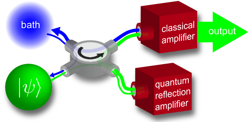
As superconducting qubit experiments scale in complexity, further signal processing innovations are needed to preserve the high level of control demonstrated in few-qubit experiments. One bottle-neck in this area is the task of unidirectional signal routing. Enforcing one-way signal propagation is critical, for example, in the separation of incoming and outgoing fields for quantum-limited reflection amplifiers, or the isolation of sensitive quantum devices from the back-action of the microwave receiver (Fig. 1).
Currently, these tasks are performed by commercial ferrite junction circulators. These devices violate Lorentz reciprocity—the symmetry, in an electrical network, under exchange of source and detector Pozar (2012)—with large permanent magnets ( mT stray fields) and the Faraday effect Fay and Comstock (1965). Unfortunately, their size and reliance on these magnets make ferrite circulators difficult to integrate on-chip with superconducting circuits, and unattractive for long-term applications in networks with many superconducting qubits.
Recognition of the need for a scalable circulator has therefore motivated the investigation of alternate means for generating non-reciprocity, using, for example, the quantum Hall effect Viola and DiVincenzo (2014); Mahoney et al. (2017a, b) and active devices Anderson and Newcomb (1965, 1966); Kamal et al. (2011); Metelmann and Clerk (2015); Kerckhoff et al. (2015); Abdo et al. (2014); Estep et al. (2014); Ranzani and Aumentado (2015); Sliwa et al. (2015); Lecocq et al. (2017); Abdo et al. (2017); Bernier et al. (2017); Peterson et al. (2017); Barzanjeh et al. (2017); Metelmann and Türeci (2017); Khorasani (2017). All of these approaches are chip-based, or can be adapted for chip-based implementations. Scalability, however, requires more than miniaturization. An ideal replacement technology would be both monolithic and operable without high-bandwidth control lines, which are a limited resource in cryogenic microwave experiments. It would also be low loss, linear at power levels typical for qubit readout and amplification, and flexible, in the sense that it should either be broadband, like a commercial circulator, or tunable over a wide frequency range, like some Josephson parametric amplifiers Castellanos-Beltran and Lehnert (2007); Mutus et al. (2013).
Here we present the performance of a superconducting microwave circulator proposed in Ref. Kerckhoff et al. (2015), which meets these stringent requirements. The non-reciprocity is created with a combination of frequency conversion and delay, which ultimately preserves the frequency of the input signal. Its operation requires no microwave frequency control tones, its center frequency may be tuned over a range of several GHz, and the device is realized on a 4 mm chip fabricated with a high-yield Nb/AlOx/Nb trilayer process Sauvageau et al. (1995); Mates et al. (2008). We first describe its theory of operation and its superconducting realization. We then present experimental results, including measurements of the circulator’s scattering matrix elements and a characterization of its transmission spectrum and linearity. These measurements are performed over a range of different operation frequencies and with the circulator configured for clockwise and counterclockwise circulation, highlighting the device’s tunability and the capability to dynamically reconfigure its sense of circulation in-situ.
II Theory of Operation
The circulator presented in this paper may be understood in terms of “synthetic rotation” created by the active modulation of the circuit, and analyzed with lumped-element circuit theory or an input-output formalism Kerckhoff et al. (2015). Here we provide a complementary explanation of its operation based upon the frequency-domain dynamics of an analogous model system.
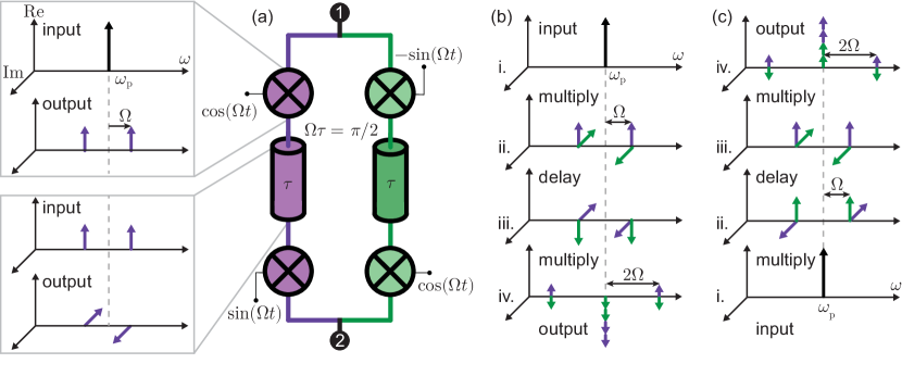
The model is a lumped-element network of multipliers and delays (Fig. 2a) which creates the most fundamental non-reciprocal circuit element: a gyrator Tellegen (1948). In a framework where electromagnetic fields propagate in guided modes into and out of a bounded network at ports, the effect of a network can be described by its scattering matrix element , the ratio of the outgoing field at port to the incident field at port Pozar (2012). Gyrators are linear two-port networks defined by the scattering matrix Pozar (2012)
| (1) |
In a gyrator, non-reciprocity is manifest in the form of a phase shift. Fields incident on port are transmitted with their phase unchanged, but fields incident on port are transmitted with a phase shift.
Gyration in the model system arises from the non-commutation of successive translations in frequency and time Rosenthal et al. (2017): the multiplying circuits operate as frequency converters, translating an input signal up and down in frequency, and the delays translate fields forward in time. As frequency and time are Fourier duals, the time-ordering of these translations matters (the two operations do not generally commute). Transmission through the network thus depends on the propagation direction of the incident signal, breaking Lorentz reciprocity.
To see that non-reciprocity explicitly, frequency-phase diagrams are used to calculate the model’s scattering parameters. The diagrams follow an incident signal at frequency as it propagates through the device, tracking its amplitude, frequency, and phase in a frame rotating at .
The insets in Fig. 2a depict the way that the model system’s two constituent elements: multipliers and delays, transform input fields to output fields. In the multiplying elements, that transformation occurs via multiplication by a bias signal—in this case, . In the frequency domain, this multiplication creates two sidebands, each detuned from by the bias frequency . Importantly, the phases of these sidebands depend on the phase of the multiplier’s bias signal. We choose a phase reference such that multiplication by creates two sidebands with the same phase.
In the delay elements, inputs are transformed to outputs by way of a phase shift. In the rotating frame, a delay of length advances the phase of spectral components in the upper sideband by , and retards the phase of components in the lower sideband by .
With the action of the multiplying and delay elements defined, calculation of the scattering parameters is straightforward. Forward transmission through the model system is shown in Fig. 2b. A signal incident on port 1 with frequency (Fig. 2b, i.) is first divided equally into the network’s two arms. Fields in both arms encounter a first multiplying element, a delay, a second multiplying element, and are then recombined.
Critically, the modulation sidebands at created in the network’s two arms are out of phase and interfere destructively at the device’s output (Fig. 2b, iv). Conversely, the components at the frequency interfere constructively. Comparison of Fig. 2b, iv. with Fig. 2b, i. shows that the incident signal has been transmitted through the device with its frequency and amplitude unchanged, but its phase shifted by . The scattering parameter for the network is therefore .
The reverse path is traced out in Fig. 2c, for a signal incident on the network’s second port. As with forward transmission, destructive interference occurs at (Fig. 2c, iv.). Likewise, this is accompanied by constructive interference at the frequency . Now, however, comparison of Fig. 2c, iv. with Fig. 2c, i. shows that the frequency, amplitude, and phase of the incident signal were unchanged by the network. Therefore, in contrast to the forward transmission, the backwards transmission is characterized by a scattering parameter . The network in Fig. 2a is thus described by the scattering matrix of Eq. (1), and forms an ideal gyrator.
The convert-delay-convert process happens simultaneously in both arms of the network. Consequently, each arm is individually non-reciprocal. Alone, though, a single arm creates unwanted modulation sidebands. To create an ideal gyrator, two arms, with the bias signals of their multiplying elements separated in phase by , are connected in parallel. This balanced architecture engineers destructive interference of the spectral components at .
Such a strategy for suppressing the creation of spurious sidebands, which we refer to as “coherent cancellation,” may be contrasted with that used in non-reciprocal devices that operate with the parametric coupling of resonant modes in the resolved-sideband limit Abdo et al. (2014); Estep et al. (2014); Ranzani and Aumentado (2015); Sliwa et al. (2015); Lecocq et al. (2017); Abdo et al. (2017); Bernier et al. (2017); Peterson et al. (2017); Barzanjeh et al. (2017); Metelmann and Türeci (2017). In that scheme, parametric modulation of a resonant system creates sidebands at the parametric drive frequency, and a second resonant mode is used to enhance the density of states at the desired frequency, while simultaneously diminishing it at the undesired frequency. To work in the resolved sideband limit, however, the parametric modulation must be many times the resonant system’s linewidth. In microwave frequency implementations, this typically requires GHz modulation tones. In contrast, the coherent cancellation approach lifts the resolved-sideband constraint, and can therefore be used with lower-frequency control tones.
III Superconducting Implementation
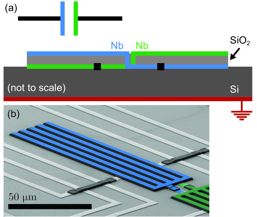
We make use of the unique properties of superconducting circuitry to realize compact on-chip multiplier and delay elements. Specifically, Josephson junctions form widely tunable inductors, while vanishing conductor loss permits on-chip high quality microwave resonators. Fig. 3 shows how a single arm of the model system (Fig. 3a) is made with a network of capacitors and dynamically tunable inductors (Fig. 3b).
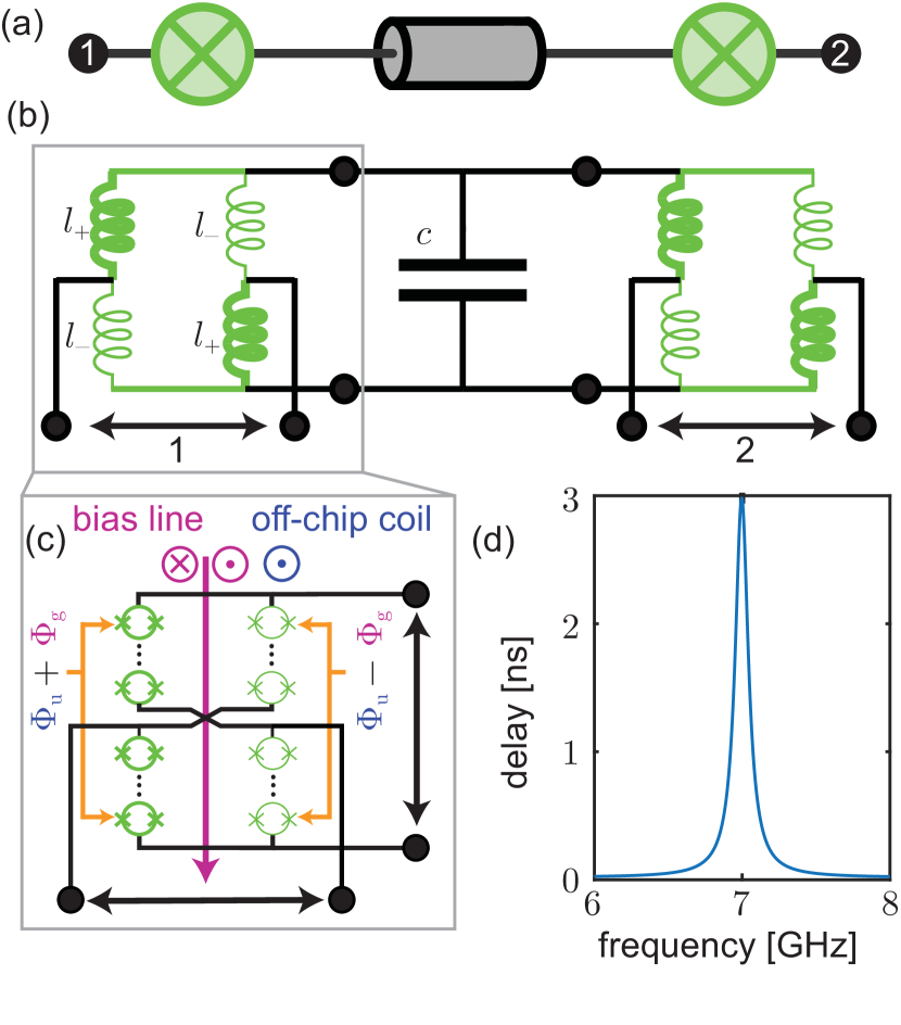
III.1 Multiplying elements
The multiplying elements in the circuit representation are created with reactive bridge circuits, built with two tunable pairs of nominally identical inductors and arranged opposite one-another (gray box in Fig. 3b). Two differential ports are defined by the left-and-right and top-and-bottom bridge nodes. Importantly, the inductors tune in a coordinated fashion: when one pair of inductors increases, the other pair decreases. We parametrize this tuning with a base inductance and an imbalance variable , by writing
| (2) |
As the imbalance in the bridge determines its transmission, changing allows the circuit to act as a switch or a multiplying element Chapman et al. (2016, 2017).
The bridge circuit’s tunable inductors are realized with series-arrays of superconducting quantum interference devices (SQUIDs), formed by the parallel arrangement of two Josephson junctions. Arrays are used in place of individual SQUIDs to increase the linearity of the inductors Kerckhoff et al. (2015). The inductance of an SQUID array depends on the magnetic flux that threads through each SQUID Likharev (1986):
| (3) |
Here is the reduced flux quantum, is the Josephson junction critical current, and the junctions and SQUIDs are assumed to be identical
To realize the coordinated tuning of inductors described in Eq. (2), we arrange the SQUID arrays in a figure-eight geometry (Fig. 3c). Two flux controls determine the imbalance in the bridge. First, an off-chip coil threads a uniform magnetic flux through all the SQUIDs. Second, an on-chip bias line, which bisects the figure-eight, threads a gradiometric flux through the SQUIDs. SQUIDs on the left side of the bias line therefore experience an overall magnetic flux which is the sum of the uniform and gradiometric contributions, whereas SQUIDs to the right of the line are threaded by the difference of the uniform and gradiometric fluxes.
When the gradiometric bias line is driven with a sinusoidal current source at frequency , the flux through the SQUIDs varies in time as . This process creates a bridge of inductors which tune according to Eq. (2), with a simple sinusoidal variation in the imbalance and a rescaling of the base inductance . App. A describes the mapping between the flux controls , and the circuit parameters , .
III.2 Delays
The second primitive needed for the model system is a delay, realized in our circuit with a resonant mode. Conveniently, the SQUIDs in the bridge circuits are inductive, so the addition of a single capacitor is enough to create a resonance. This resonance delays fields near its center frequency by a timescale characterized by the inverse of its linewidth. More quantitatively, when a harmonic field incident on port of a resonant network is scattered to port , it acquires a group delay Pozar (2012). Here is the frequency of the harmonic field, and is the phase of . Fig. 3d shows delay as a function of frequency, for the resonant circuit in Fig. 3b. Fields near the circuit’s resonant frequency experience a delay of several nanoseconds.
Delays realized with resonant modes allow for a deeply sub-wavelength implementation, which is critical for the “coherent cancellation” approach. While these lumped-element delays are necessarily narrower in bandwidth than those created with a length of transmission line, their finite bandwidth is mitigated by the tunable inductance of the bridge circuits, which allows the frequency of the resonant delay to be tuned (over several GHz) with the uniform magnetic flux . As the multiplying elements are broadband Chapman et al. (2017), this tunability of the delay is inherited by the full circulator. Likewise, the duration of the delay depends on the imbalance in the bridges, and may be tuned with the gradiometric flux , facilitating satisfaction of the requirement that .
Tuning of the resonant delay takes a simple form when expressed in terms of the circuit parameters and . When two of the arms in Fig. 3b are combined in parallel to create the fully assembled circuit shown in Fig. 4a, the resonant delay occurs at the frequency Kerckhoff et al. (2015)
| (4) |
and its duration is approximately the inverse of the resonant mode’s linewidth,
| (5) |
Here is the characteristic impedance of the surrounding transmission lines.
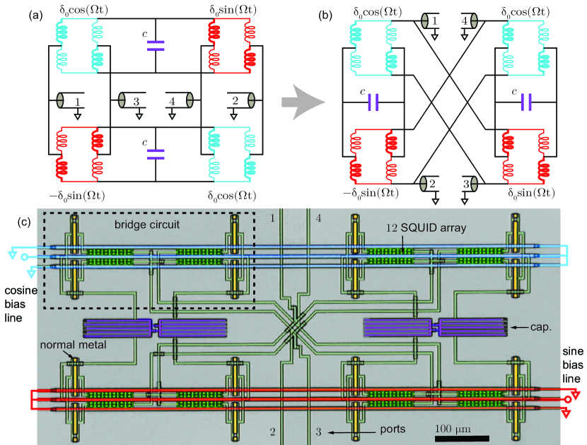
III.3 Circulator
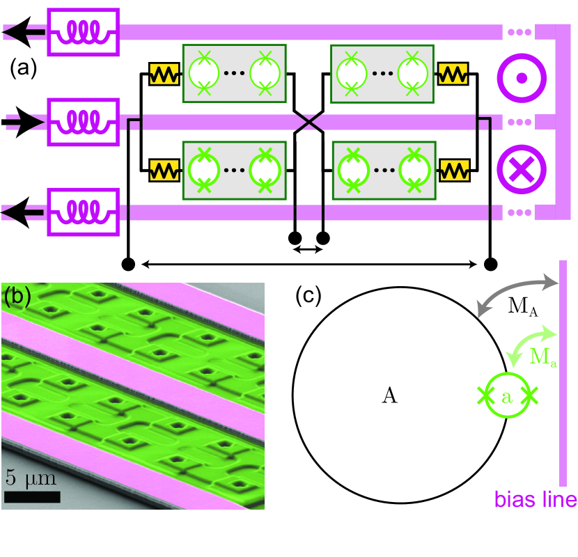
Assembly of a superconducting version of the full circuit requires the parallel combination of two arms like the one shown in Fig. 3b. Fig. 4a shows a lumped element schematic of the complete network. When ports 1 3 and 2 & 4 are driven differentially, the circuit in Fig. 4a creates a gyrator that functions in the same way as the model system (Fig. 2a). If instead, however, ports are defined by comparison of voltages to a common ground (as shown in Fig. 4a), the circuit forms a reconfigurable four-port circulator, with (ideal) clockwise scattering matrix:
| (10) |
or counterclockwise scattering matrix .
The transformation between gyrator and circulator can be understood in the following way: driving any one of the device’s four ports involves simultaneously exciting the common and differential modes of the circuit. The gyrating differential mode is non-reciprocal, whereas the prompt scattering of the non-resonant common mode is reciprocal. The interference of these two scattering processes results in circulation Kerckhoff et al. (2015).
For fabrication, the circuit is laid-out as illustrated in Fig. 4b. This rearrangement leaves the connectivity of the circuitry unchanged, but allows two pairs of parallel flux-control bias lines to bisect the four inductive bridges. Fig. 4c shows a false-color optical micrograph of the device, laid out in this way.
The SQUID arrays that comprise the circuit’s multiplying elements are colored dark green in the micrograph and oriented horizontally. Capacitors, to make the resonant delays, are realized in a parallel-plate, metal-insulator-metal geometry, and colored purple. Finally, normal metal (Au) is used in the layout to break supercurrent loops which can trap flux. These sections are colored gold, and have a resistance of approximately milliohms, which increases insertion loss by 0.1 dB. Further details on the layout design considerations are provided in App. D.
IV Experimental Results
To test the device, two of its four ports are terminated in Ohm loads and the circuit is mounted at the base of a 3He cryostat. A schematic of the experimental setup is shown in Fig. 5. Two switches and a directional coupler allow for measurement of the four accessible scattering parameters.
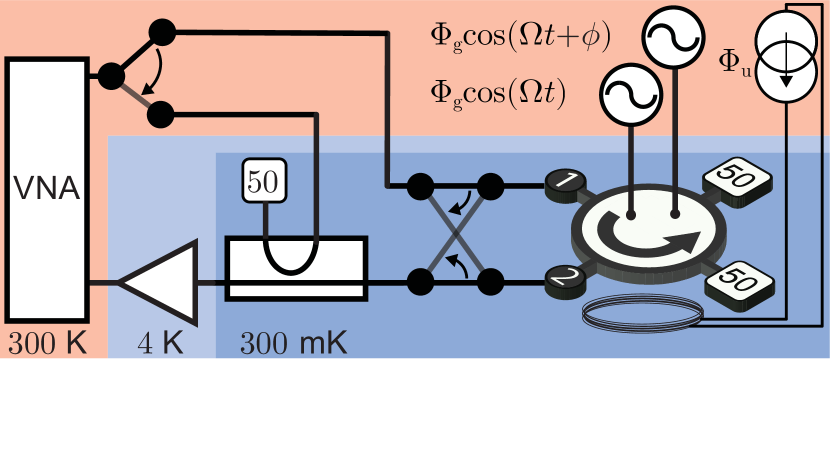
App. B describes the tune-up procedure, which involves choice of the modulation frequency and the delay , as well as selection of the phases and that best accomplish clockwise and counterclockwise circulation. Fig. 6 shows the results of this process, when the device is tuned to operate near 4 GHz. Four of the device’s sixteen scattering parameters are plotted in Fig. 6a, for both the clockwise and counterclockwise operation modes. Different ports were probed in a separate cooldown, with similar results. (Calibration of network parameter measurements is discussed in App. C.)
In the transmission measurements (top right and bottom left plots), high transmission ( dB) and robust isolation ( dB) are observed in a MHz window around GHz. These features are approximately coincident with dB dips in the reflection measurements (top left and bottom right plots). Together, power collected in the transmission and reflection measurements account for 90% of the injected signal power.
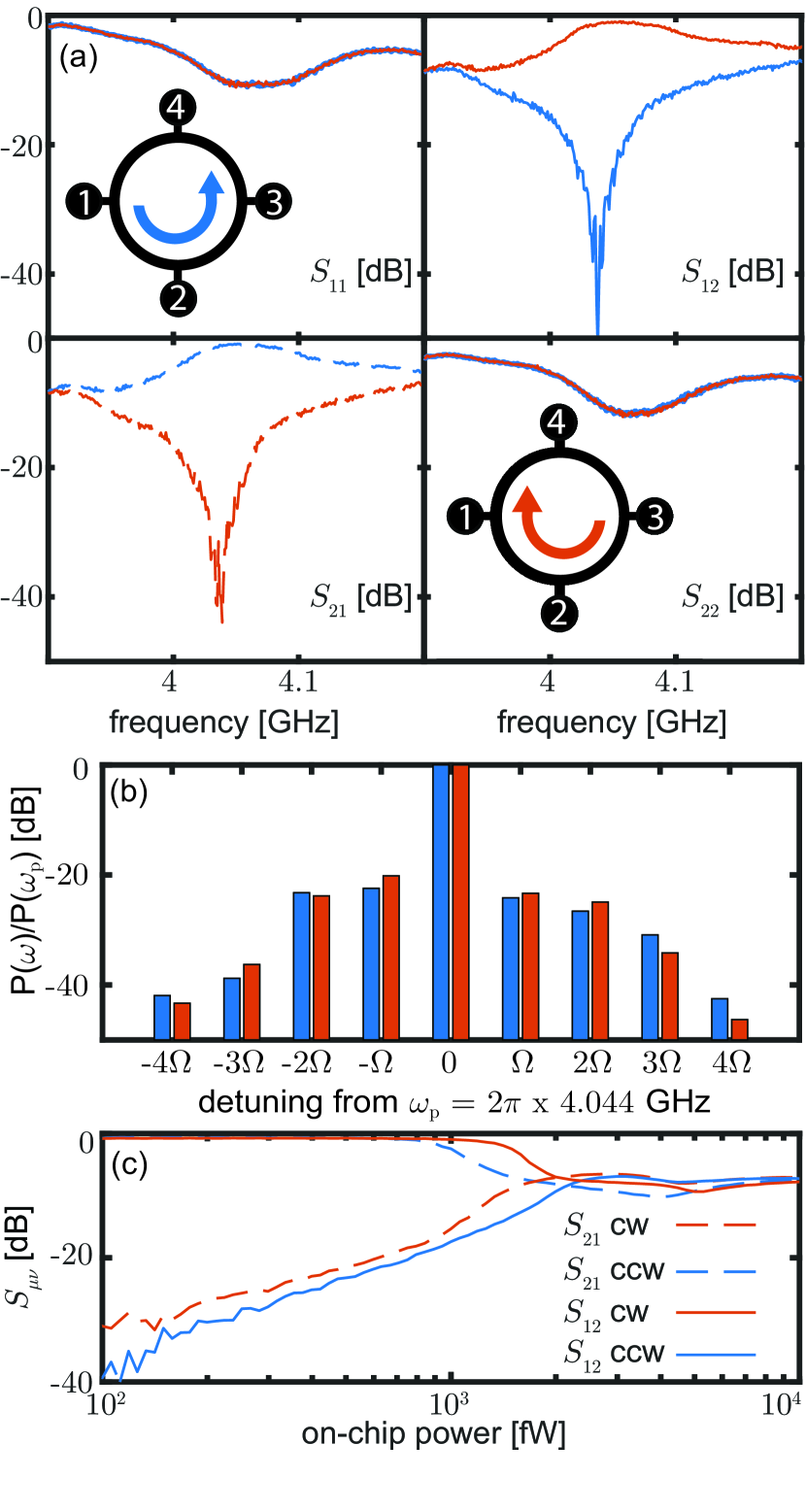
To determine if the remaining power is dissipated or scattered to other frequencies, a spectrum analyzer is used to measure the transmission of the circulator at sidebands of the modulation frequency . Fig. 6b shows the power of these spectral components, relative to the transmitted spectral component at . The device suppresses spurious sidebands by more than 20 dB. The spectral purity of the output—in particular, the suppression of spectral components at —is a testament to the high-degree of symmetry in the circuit. From this measurement, we conclude that the remaining 10% of input power is dissipated into heat or other radiation modes.
Finally, Fig. 6c displays the dependence of clockwise and counterclockwise transmission on the power of the probe signal. Fixing the probe frequency at GHz, the measurement is repeated for both clockwise and counterclockwise operation. In both cases, 1 dB compression of the transmitted signal occurs at input powers around 1 pW. As the input power approaches this value, we also observe a degradation in the circulator’s isolation, which drops below 20 dB at a power again roughly equal to 1 pW. In analogy with the 1 dB compression point, we refer to this power as the 20 dB expansion point of the circulator. Expressed in terms of photon number, this linearity allows the circulator to process over photons per inverse of its bandwidth.
For reference, the typical power in a microwave tone used for dispersive readout Blais et al. (2004) of a superconducting qubit is between and aW (few photon level) Riste et al. (2013). The three orders of magnitude that separate this power scale from the 1 dB compression and 20 dB expansion points of the device are critical for one attractive application of a monolithic superconducting circulator: on-chip integration with a quantum-limited reflection amplifier, such as a Josephson parametric amplifier. The high power handling of the circulator allows it to route qubit readout tones even after they reflect off a Josephson parametric amplifier and are amplified by 20 dB.
To demonstrate the circulator’s tunability, we operate the device at a variety of frequencies between 4 and 6 GHz and repeat the measurements shown in Fig. 6. Fig. 7 summarizes the performance of the device across this tunable range. Insertion loss is shown in Fig. 7a. Transmission is greatest at the lowest frequency, and decreases with frequency until it approaches -3 dB. We attribute this trend to the geometric inductance present in the circuit, which limits the degree to which the bridges can be imbalanced. This inhibits impedance matching and reduces the degree to which the resonant differential modes are over-coupled. At lower operation frequencies, the Josephson inductance comprises a greater fraction of the bridge’s total inductance, mitigating this effect.
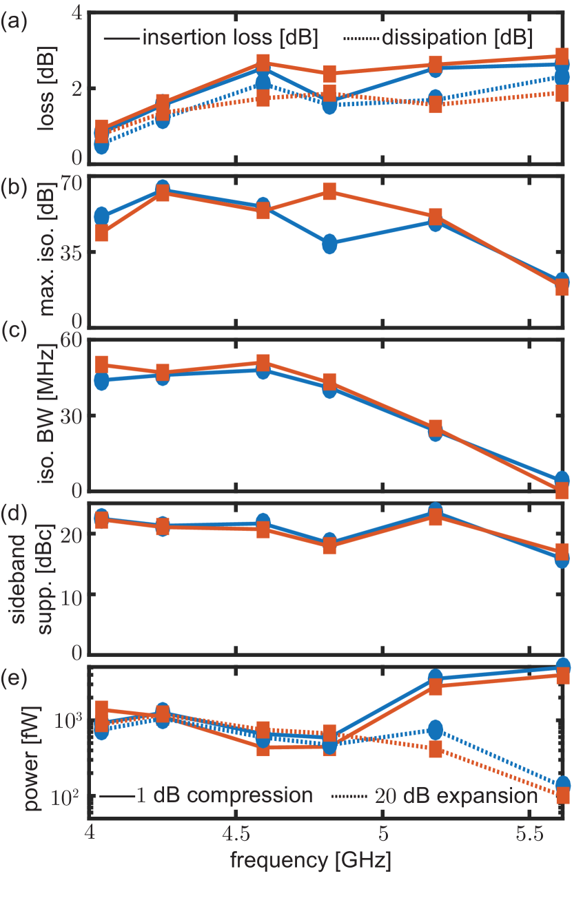
This interpretation is supported by the power dissipation that we estimate at each operation frequency (Fig. 7a, dashed lines), computed as the sum of the reflection and transmission coefficients . (Power transmitted to sidebands of the modulation frequency is suppressed by over 20 dB, and is therefore neglected in this accounting). Reflections, visible in the discrepancy between insertion loss and transmission, are larger at higher frequencies, where the role of geometric inductance is more pronounced. Dissipation is also greater at higher operation frequencies, where the external coupling of the resonant mode is lower. One of the principal dissipation sources in the circuit is the dielectric loss of SiO2, which results in a frequency-dependent loss that we estimate ranges from 0.3 to 0.8 dB.
The circulator’s maximum isolation is plotted in Fig. 7b. Below 5.5 GHz, isolation exceeds 35 dB for both device configurations. Critically, isolation is achieved over a bandwidth of several tens of MHz, much greater than the bandwidths typical for strongly-coupled cavity ports in dispersive qubit readout, which range up to several MHz Kelly et al. (2015); Ofek et al. (2016); Hacohen-Gourgy et al. (2016). Fig. 7c shows the frequency interval over which the isolation exceeds 20 dB.
It should be noted this isolation is achieved concurrent with the performance shown in the rest of Fig. 7: all specifications are measured at two fixed operation phases, which realize clockwise and counterclockwise circulation. To select these operation phases in a quantitative manner, we write a cost function to simultaneously balance the benefits of low insertion loss, high isolation, and broad bandwidth, for both clockwise and counterclockwise operation. Ultimately, different applications will prioritize the relative importance of these specifications in different ways, allowing trade-offs in performance specifications, for example, between insertion loss and isolation. Similarly, if the device’s reconfigurability is not needed, performance will generally exceed that shown in Fig. 7.
Fig. 7d characterizes the spectral purity of transmitted fields at each operation frequency. It shows the size of the largest spurious sideband, (relative to the power transmitted at the probe frequency), which we call the sideband suppression. Spurious sidebands are strongly suppressed across the operation range, typically by about 20 dB.
Lastly, Fig. 7e shows how the power-handling of the circulator depends on the operation frequency. Frequencies between 4 and 5 GHz have 1 dB compression points and 20 dB expansion points around 1 pW.
V Conclusion and Outlook
In this work we realize the on-chip superconducting circulator proposed in Ref. Kerckhoff et al. (2015). Lorentz reciprocity is broken in the circuit with sequential translations in frequency and time, which we show with a simple model system composed of just two components: multiplying elements and delays. We describe how both elements can be created in a cryogenic microwave environment, and then characterize the performance of a circulator built from these components. We observe low insertion loss and over dB of isolation over a bandwidth of approximately 50 MHz. The device is linear with respect to input power for fields up to pW in power, and its transmission spectrum is spectrally pure, in the sense that spurious harmonics created by the device’s RF control tones are suppressed by more than dB. Finally, we demonstrate that all of these performance specifications can be achieved over a tunable operating range approaching GHz, and in clockwise or counterclockwise configurations.
As the device is controlled with radio frequency tones (which are a) easily phase-locked and b) require none of the limited high-bandwidth transmission lines in a dilution refrigerator), and as it is orders of magnitude more compact than commercial ferrite circulators, this superconducting circulator is a scalable alternative to signal routing with ferrite junction circulators. We estimate that with superconducting twisted pairs carrying the low-frequency control tones, of these circulators could be operated in a single dilution refrigerator (see App. F).
Looking forward, the work suggests several immediate extensions. In a future design, layout changes could improve device performance: dielectric loss can be reduced with the use of low-loss dielectrics like amorphous silicon Lecocq et al. (2017) or interdigitated capacitors. Similarly, dividing the power in the gradiometric flux lines off-chip and delivering them on-chip in four dedicated bias lines removes layout constraints, and enables the design of a circuit with approximately half the geometric inductance. Even with the device’s existing performance, another obvious extension is on-chip integration of the circulator with a quantum-limited amplifier, for measurements of added noise. Finally, the essential concept of frequency conversion and delay can be adapted to a lossless and broadband design, using non-resonant delays Doerr et al. (2011); Yang et al. (2014); Rosenthal et al. (2017). Prospects for such a device are extremely attractive given the high power-handling of these SQUID-array based devices, as their integration with a broadband low-noise amplifier Macklin et al. (2015) could enable scalable frequency-domain multiplexing of many-qubit systems with near-unit measurement efficiency.
Acknowledgments
This work is supported by the ARO under contract W911NF-14-1-0079 and the National Science Foundation under Grant Number 1125844.
Appendix A Flux control
The proposal in Ref. Kerckhoff et al. (2015) analyzes a lumped-element model of the circulator, formed with dynamically tunable inductors parametrized according to Eq. (2). The following relations connect that parametrization with the experimental flux-control parameters and Lalumière (2015):
| (11) |
with
| (12) |
and the Bessel function of the first kind.
Appendix B Tune-up procedure
Three straightforward steps are required to prepare the circulator for operation. First, the frequency of the resonant delay is tuned to the desired operation frequency. Second, the duration of the resonant delay is set to . Finally, the phase difference between the gradiometric flux control drives is set to .
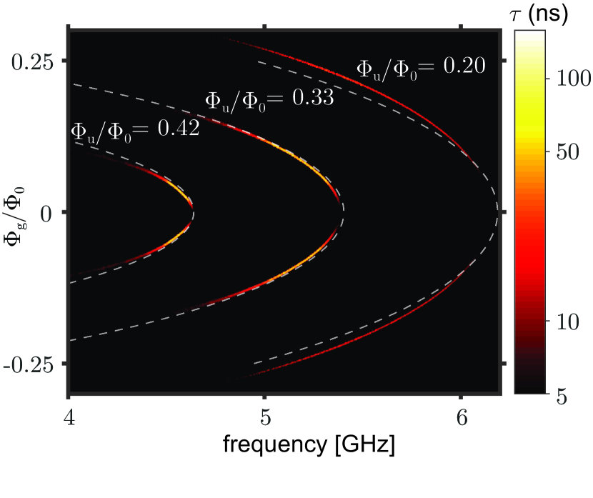
We illustrate the first two of these steps in Fig. 8, which shows in color the group delay acquired during transmission through the device at different probe frequencies , and for different values of a static gradiometric flux applied to all four of the inductive bridges. The measurement is shown for three different values of the uniform flux .
Two features are immediately evident in the data. First, the resonant nature of the delay is clear: for fixed values of and , fields at most probe frequencies are off-resonance and their group delays are less than 5 ns, as visible in the black background of the color plot. Against this background, three arches are visible, which show the resonant delay tuning with for the three measurements at distinct . The shapes of these arches are qualitatively captured by the theoretical predictions in dashed gray lines, which are made with Eq. (4) and the relations in App. A that map & to & .
Second, when approaches , the group delay vanishes. A gradiometric bias with magnitude much less than results in approximately balanced bridges (). As the external-coupling of the resonant mode depends on (Eq. (5)), balanced bridges result in under-coupled resonant modes, which strongly attenuates transmission through the resonant differential modes. (The internal quality factor of the circuit is estimated to be 400 when the resonant delay is tuned to 5 GHz.) Power is still transmitted through the non-resonant common mode, but without acquiring resonant delay.
As circulation bandwidth scales with the linewidth of the resonant delay, for the measurements in this paper we operate the device with a relatively brief delay on the order of several nanoseconds, with MHz. This choice has the additional benefit of reducing the influence of internal losses by keeping the circuit strongly over-coupled.
The final step of the tune-up procedure involves selection of the relative phase between the gradiometric flux controls. Fig. 9 shows a sweep of when the resonant delay is set near GHz and the duration of the delay is fixed at several ns with MHz. The color scale in Fig. 9a shows the magnitude of as a function of this phase and the probe frequency: is shown in Fig. 9b.
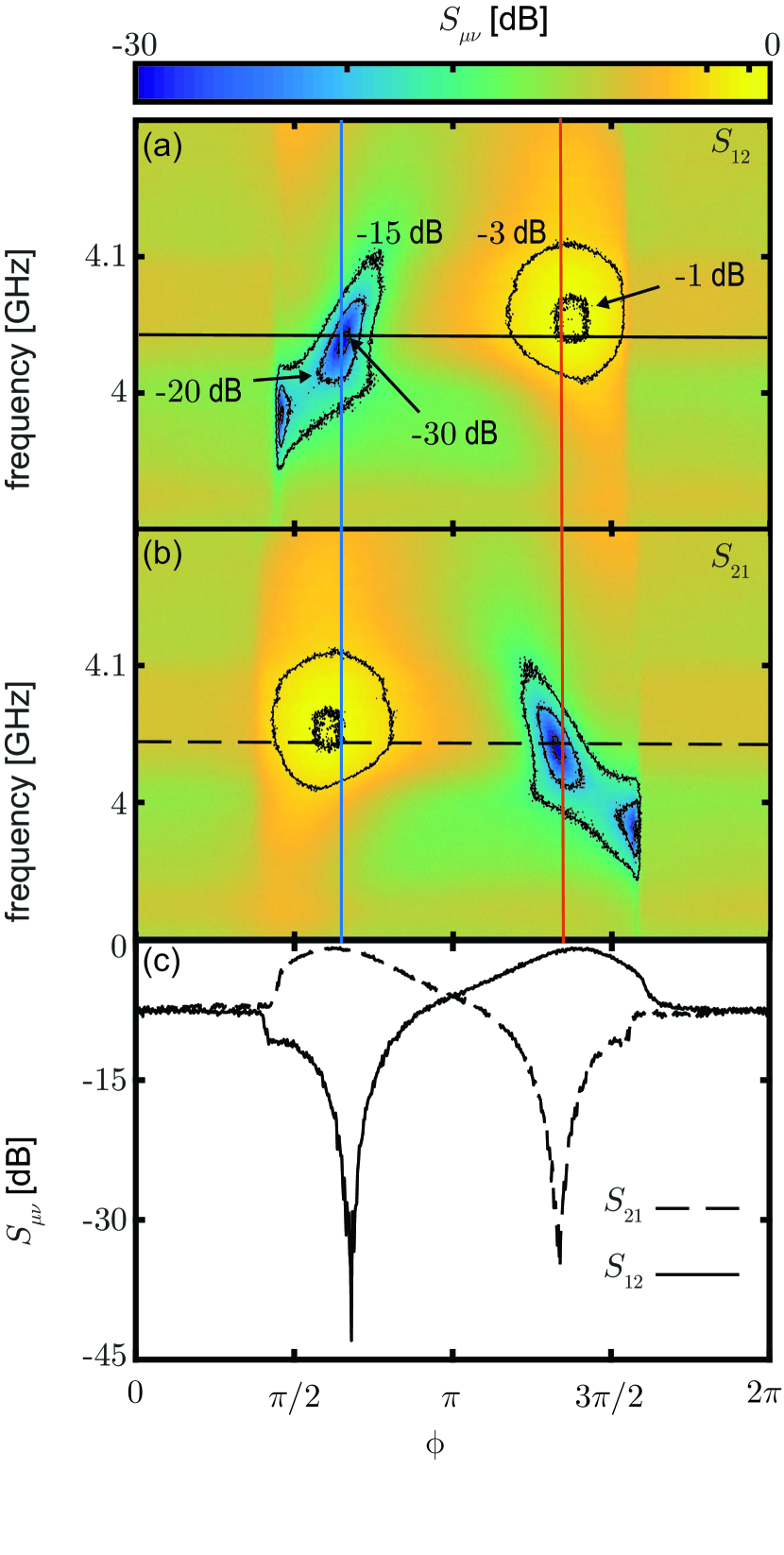
The color plots in Fig. 9 reveal two regions of parameter space in which operating points can be chosen. At these phases, the insertion loss is less than 1 dB and the isolation exceeds 30 dB. They can therefore be interpreted as the phases which realize a clockwise or counterclockwise circulator. To illustrate this, Fig. 9c shows frequency linecuts at GHz from both transmission measurements. Importantly, the linecuts show that high transmission in the counterclockwise (clockwise) direction is accompanied by strong isolation in the clockwise (counterclockwise) direction. They also illustrate how toggling the phase allows dynamical reconfiguration of the device’s sense of circulation. Interestingly, one can see that the strongest non-reciprocity is observed at phases near but distinct from the expected operating points at and . App. E describes how geometric inductance in the circuit causes this discrepancy.
Appendix C Calibration of network parameter measurements
C.1 Transmission calibration
To remove the gain of the measurement chain in transmission measurements, a bypass switch is mounted at the base of the cryostat, which routes fields through a 5 cm SMA cable instead of the circulator. We also use dedicated through measurements, (made in a separate cooldown) in which the circulator chip is exchanged for a like-sized circuit board traversed by a single 50 Ohm transmission line. Using these techniques, the reference plane for transmission measurements is moved (approximately) to the edge of the chip.
C.2 Reflection calibration
To remove the gain from reflection measurements, we measure the reflection off the circulator when no bias current is applied to the on-chip bias lines. In this unbiased state, all four inductor bridges are balanced, and the reflection coefficient is the diagonal entry in each row of the balanced scattering matrix . The matrix may be calculated by substituting the lower-right block matrix of Eq. (8) in Ref. 19 into Eq. (19) of that reference. This procedure yields
| (13) |
As
| (14) |
and the gain of the reflection measurement chain is assumed to be independent of the circulator’s state, the reflection coefficient at arbitrary operation points is related to the measured reflection by
| (15) |
C.3 Calibration of group delay
Preparing the circulator for operation requires correctly setting the duration of the resonant delay. Measurements of the circulator’s group delay are used for this purpose. To separate the non-resonant delays of the finite-length measurement chain from the resonant delay , we multiply the measured transmission data by , where ns is the time required for an off-resonant microwave field to propagate through the measurement chain. In the absence of circuit resonances, this multiplication makes the phase of the transmission flat as a function of frequency, zeroing the group delay.
Appendix D Circuit layout
The circuit discussed in this work presents several design challenges, some of which are specific to superconducting circuits.
D.1 Capacitor design
To realize the capacitors in the circulator’s lumped element representation (Fig. 4a), we layout parallel-plate capacitors in a metal-insulator-metal geometry with Nb plates sandwiched around the dielectric SiO2 (Fig. 10a). In the frequency range of 4 to 8 GHz, roughly pF capacitances are required to create capacitor-impedances near 50 ohms. Making a pF capacitor with SiO2 in the Nb trilayer process requires capacitor plates that are roughly 100 m on a side—large enough to trap magnetic flux vortices when cooled through Niobium’s superconducting transition temperature in earth’s magnetic field Stan et al. (2004).
To avoid trapping flux vortices, we pattern slots in the capacitor electrodes, such that the Nb strips that form the electrodes never exceed a width 100 m . This ability to suppress vortices in non-zero magnetic fields is important for our layout, as the circulator is actuated with flux controls which can be spoiled by a static and unremovable flux gradient. Choosing m ensures that the capacitor electrodes trap no magnetic flux vortices when the capacitor is cooled through in our experiment’s modestly shielded magnetic environment.
To further symmetrize the circuit, each parallel-plate capacitor is then divided into two capacitors of capacitance , and connected in parallel, such that the upper plate of the first (second) capacitor is galvanically linked to the lower plate of the second (first) capacitor (Fig. 10b). This procedure gives each side of the composite capacitor the same parasitic capacitance to ground, and is essential for preserving the symmetry on which the concept of the device relies.
A scanning electron microscope image of a capacitor is shown in Fig. 10b, which shows the Nb strips that form the top plate of one of the parallel plate capacitors. In the right side of the image, the capacitor is connected to a second parallel plate capacitor (mostly out of view) in the manner described above.
D.2 Use of normal metal
Superconducting loops in the circulator can trap magnetic flux and lead to an unstable flux environment, interfering with the flux biasing used to control the device. To avoid trapping unwanted flux, we layout the circulator using small amounts of a normal metal (Au). The thickness (height) of the gold layer is nm, giving it a sheet resistance of milliohms/square. To reduce resistive losses in this layer, 11 Au squares are placed in parallel, yielding a total film resistance of about 10 milliohms. Four of these resistors are placed in each Wheatstone bridge (yellow rectangles in Fig. 4c and resistor symbols in Fig. 11b) to break supercurrent loops and maintain the symmetry required by the circuit. Estimates with time-domain numerical simulations (Simulink) indicate that the addition of these resistors causes the dissipation in the circuit to increase by 0.1 dB, limiting the internal of the circuit to be less than 2000.
To design the normal metal resistors in a way that prevents proximitization by the nearby niobium, the resistor lengths —defined as its dimension parallel to the flow of current—is constrained to be . Here is the coherence length of Au calculated in a dirty limit, where the metal film’s mean free path is less than the clean-limit coherence length Van Duzer and Turner (1981)
| (16) |
In the above, is the Fermi-velocity of the metal, is Boltzmann’s constant, and is the metal’s temperature. We justify this treatment with the observation that the Au film’s mean free path nm m . This estimate for is made with the assumption that m/s in Au Ashcroft and Mermin (1976), and the temperature set to 300 mK. The mean free path is calculated with the Drude model Ashcroft and Mermin (1976) and the film’s resistivity.
In the dirty-limit, the coherence length is essentially a geometric mean of the clean-limit coherence length and the metal’s mean free path Van Duzer and Turner (1981):
| (17) |
which comes out to m for the above values of and . This value is comparable with measurements of the dirty-limit coherence length in thin films of a similar elemental metal, copper, when one corrects for sample thickness Pothier et al. (1994); Dubos et al. (2001).
The condition can be made quantitative with consideration of the superconducting-normal-superconducting (SNS) junction physics which govern the Nb-Au-Nb interface. Unlike a superconducting-insulator-superconducting junction, which is governed by an energy scale set by the superconducting gap, the natural energy scale for the proximity effect in an SNS junction is the Thouless energy Dubos et al. (2001). For junctions of reasonable size (), the critical current of the SNS junction is
| (18) |
Here is the electron charge, m is the inelastic scattering length of gold at 300 mK Mohanty and Webb (2003), and the Thouless energy is expressed in terms of the coherence length and the junction length . The critical current sets the Josephson energy of the SNS junction, and the resistance of the junction scales in relation to the Josephson energy and the energy in the thermal environment:
| (19) |
Along with the Josephson inductance of a SQUID array (Eq. (3)), the resistance in Eq. (19) sets an time which characterizes the time required for trapped-flux to dissipate out of the circuit. Choosing ensures that time is less than 1 second. In preliminary designs, we therefore set m . In later designs we found experimentally that m also prevents flux-trapping, likely due to a dirty-limit coherence length which is less than our 1 m estimate. The device presented here has m .
D.3 Bias line design
The circulator’s active components are actuated with flux controls created by a pair of on-chip bias lines. Design of these bias lines involves two important layout considerations: namely, isolating the microwave fields from the bias lines, and preventing the RF bias signals from interfering with the operation of the microwave circuit.
Isolating the circulator’s microwave fields from the bias lines is important because from the perspective of the microwave circuit, coupling to the bias lines acts as an additional loss channel. To reduce losses of this kind low-pass filters (20 nH spiral inductors) are inserted into the bias lines as they enter and exit the chip (pink inductor symbols in Fig. 11a). These simple filters present an impedance of approximately 15 ohms to the bias signals at MHz, whereas at microwave frequencies in the 4 to 8 GHz band their impedance exceeds 500 ohms. Simulations using commercial planar method-of-moments solvers (AWR Microwave Office) indicate that these filters limit microwave transmission out the bias lines to less than dB.
The challenge of the second consideration—preventing bias signals from interfering with the circuit’s microwave operation—is illustrated in Fig. 11c. The lumped-element representation of the circulator (Fig. 4a) contains tunable inductors, realized with flux-modulated SQUIDs, as well as larger circuit loops which are (partly) comprised of SQUIDs. For simplicity, we consider the effect of a bias line on one such loop of area which includes a SQUID with area inside it (Fig. 11c).
To operate the circulator, the bias line must dynamically thread a flux through the SQUID, on the order of a tenth of a flux quantum , at a rate . If the mutual inductance between the bias line and the SQUID loop is denoted as , this requires an AC bias current with amplitude .
The time-dependent gradiometric flux, however, also threads through the larger circuit loop of area . Faraday’s law describes the electromotive force induced around this loop, which for a cosinusoidal bias current is . We assume the impedance of the loop is entirely inductive in origin. The loop inductance is the sum of its geometric and Josephson inductance , which we write in terms of the participation ratio as , yielding . Ohm’s law then allows a calculation of the AC current induced around the loop of area , which with the appropriate substitutions has an amplitude of
| (20) |
with the critical current of the SQUID.
When the induced currents approach the SQUID critical currents in magnitude, the higher order corrections in Eq. (3) become significant, and when it exceeds the critical currents, the SQUIDs become dissipative elements. From Eq. (20) one can see that the bias signals will couple to the microwave circuit and interfere with the circulator’s operation unless the prefactor on the equation’s right-hand side is much less than one. The circulator’s performance (in particular, the ability to impedance match the device) requires that the participation ratio not be much greater than one. The only way to satisify the requirement, then, is to engineer the mutual inductances such that . This is challenging, as the size of the parallel plate capacitors and the SQUID arrays mandates that .
To overcome the disparity in loop areas and satisfy the coupling condition , we layout the bias lines in a symmetric way, such that their currents create magnetic quadrupoles. The layout of the shielded bias lines is shown schematically in Fig. 11a, and is also visible in the SEM image in Fig. 11b, as well as Fig. 4c. The central bias line, bisecting the bridge, carries the full bias current across the chip, and then splits into two parallel arms, each carrying a current on the outside edges of the bridge. As the currents in these lines flow in opposite directions, the magnetic field from this shielded configuration scales as
| (21) |
where is the separation between the inner and outer bias lines, and is the vacuum permeability. We make as small as possible in our layouts, given the requirement that the SQUID arrays must reside between the inner and outer bias lines. These constraints result in the choice m.
Appendix E Circulator non-idealities
In this section we discuss non-idealities observed in the circulator, in which the network parameter measurements depart from the theoretical predictions of the scattering matrix, obtained with the analytical model in Ref. Kerckhoff et al. (2015). That reference predicts the dependence of on the parameters , , and , and using the relations in App. A, and can be mapped to the flux controls and . To facilitate this comparison, Fig. 12 shows measured and predicted transmission parameters, as a function of the probe frequency and the gradiometric flux .
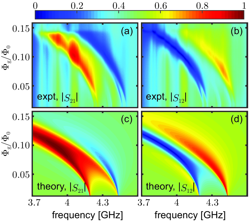
Qualitatively, the experiment and model agree fairly well: all four plots show a pair of resonant modes split by twice the modulation rate , in analogy with a Sagnac interferometer Scully and Zubairy (1997). As increases, these modes shift down in frequency and broaden. Furthermore, the device’s non-reciprocity is evident in both the model and in experiments: at the lower frequency mode, is large in magnitude at the same frequency and gradiometric flux that is small.
One can also see aspects of the experimental data which are not captured in the model. For example, as approaches the resonant modes become increasingly difficult to perceive in the experimental data. In the model, though, the modes become narrower and decreases, but remain well distinguished from the off-resonant transmission. This discrepancy is a result of the fact that internal losses are not included in the theoretical model. In the measurement, the presence of loss means that for small enough , the modes become under-coupled and are difficult to detect.
Another discrepancy is the slight splitting ( MHz), visible in the experimental plots (Fig. 12a and b), of each resonant mode. We attribute this splitting to a hybridization of the circuit’s two degenerate resonant modes, which is not included in the model.
The sharp “edge” visible at large in the measurements is an additional difference between the model and experiments. In dedicated studies of this feature, we observe that the location of the edge depends on both the frequency and the phase between the gradiometric flux drives. When the inverse of the edge’s location is plotted as a function of , it scales as , which is precisely the scaling one would expect if the edge resulted from the total flux (i.e. the interference between the two gradiometric flux lines) through a large loop in the circuit exceeding some critical value—for example, a value set by the SQUID critical currents, in the manner discussed in App. D.3. This observation supports the conjecture that the edge is caused by induced currents in the microwave circuit which exceed the critical current of the SQUIDs.
Refinements in the layout can reduce these induced currents, though device operation would still be limited in the amplitude of the applied gradiometric flux; the application of a total external flux with magnitude greater than causes a deviation from the simple flux-tunable circuit model described in Fig. 3. When the total flux exceeds this threshold, further increase in serves to balance the inductive bridges, rather than imbalance them, and a departure from the model is expected in this regime.
A final difference between the model and experiments is visible in the scaling of the resonant modes with the gradiometric flux. The modes in the theory plots are more sensitive to , bending down to lower frequencies than the measured modes. They also broaden and merge, to a degree which is not apparent in the measurements. We attribute this discrepancy to geometric inductance in the circuit which reduces the tunability of the resonant delay and restricts the modal linewidth.
This interpretation is supported by our observation of optimal circulator performance at drive phases distinct from the theoretically expected values at and . When geometric inductance restricts the linewidths of the circulator’s resonant modes, it prevents the creation of the brief (2 ns) resonant delay needed to satisfy the convert-delay operation condition: . The condition can be met with reduction of , but this is undesirable for two reasons. First, the circulator’s bandwidth is proportional to . Second, device performance requires that the modulation rate exceed the internal splitting of the hybridized resonant modes: .
A simple extension of the theory discussed in Sec. II shows how the circulator’s transmission depends on and in the general case when takes values other than :
| (22) | |||||
From these expressions, it is clear that if is forced to take values greater than , improved counterclockwise (clockwise) circulation can be obtained with phases greater (less) than (). Our observation of optimal control phases at and corresponds to a minimum achievable delay of about 3 ns.
Appendix F Filtering, attenuation, and power-consumption considerations
One of the costs associated with replacing passive ferrite circulators with active on-chip circulators is the power consumption of the control tones, and the heat loads this creates in a dilution refrigerator. Estimating that power consumption requires a discussion of the attenuation and filtering of the control lines.
To determine the attenuation required to keep the added noise below half a photon, the added noise is estimated as a function of the temperature to which the control lines are thermalized. Scaling and filtering considerations are then discussed, in light of this result.
For simplicity, consider the noise added by the circulator during transmission from its first port to its second port. Fluctuations of the bias current amplitude and relative phase between the two bias signals will modulate a transmitted tone, thus creating noisy modulation sidebands of the tone. The sideband noise powers caused by amplitude fluctuations and phase fluctuations are (at most)
| (23) |
Here, is the signal current in the device at its dB compression point and is the current spectral density of the Johnson noise (in the bias lines) at a temperature Johnson (1928); Nyquist (1928). Because we operate near a maximum in , the dominant effect of noise in both the amplitude and phase of the bias currents is to modulate the phase of the transmitted tone; i.e., both and are predominantly phase noise in the transmitted tone.
The partial derivatives in Eq. (23) can be calculated directly from measurements of the scattering parameters, made as a function of the bias current amplitude and the phase between the bias lines (shown, for example, in Fig. 12 and Fig. 9). After these numerical derivatives are calculated, the sideband noise powers may be divided by to convert them to photon numbers. In our measurements, where the bias lines are thermalized to K, this results in photons of added noise, with accounting for of the noise.
Positioning db of attenuation at room temperature and dB at the four Kelvin stage of a dilution refrigerator would result in a noise temperature of K, or in units of photons, . This level of attenuation is reasonable for modern dilution refrigerators, as the circulator operates with gradiometric currents on the scale of A: the heat load caused by a dB attenuator at the four-K stage is W, which is much less than the Watt-scale cooling power available at that stage.
With superconducting twisted-pairs to carry the bias currents from the four-K stage to the mixing chamber plate, and a contact resistance of milliohms at the chip interface, the heat load on the mixing chamber plate is pW. This load is also much less than the roughly W of available cooling power on a mK mixing chamber plate. These considerations are summarized in Tab. (1), which presents a power budget for an active circulator with control lines thermalized as described above.
| [K] | [A] | heat load [W] | cooling power [W] |
|---|---|---|---|
| 300 | n/a | ||
| 4 | |||
| 0.05 |
This analysis indicates the feasibility of operating on-chip circulators in a single dilution refrigerator, each with less than half a photon of added noise. We emphasize that it is one of many possible design choices and it is possible to reduce the added noise and dissipated power in several different ways. For example, the bias lines could be filtered to reject the noise below 50 MHz, which adds noise in the circulator’s band, while still passing 100 MHz bias tones.
References
- Blais et al. (2004) A. Blais, R.-S. Huang, A. Wallraff, S. M. Girvin, and R. J. Schoelkopf, Physical Review A 69, 062320 (2004).
- Kelly et al. (2015) J. Kelly, R. Barends, A. G. Fowler, A. Megrant, E. Jeffrey, T. C. White, D. Sank, J. Y. Mutus, B. Campbell, Y. Chen, et al., Nature 519, 66 (2015).
- Ofek et al. (2016) N. Ofek, A. Petrenko, R. Heeres, P. Reinhold, Z. Leghtas, B. Vlastakis, Y. Liu, L. Frunzio, S. Girvin, L. Jiang, M. Mirrahimi, M. H. Devoret, and R. J. Schoelkopf, Nature (2016).
- Castellanos-Beltran et al. (2008) M. A. Castellanos-Beltran, K. D. Irwin, G. C. Hilton, L. R. Vale, and K. W. Lehnert, Nature Physics 4, 929 (2008).
- Bergeal et al. (2010) N. Bergeal, R. Vijay, V. E. Manucharyan, I. Siddiqi, R. J. Schoelkopf, S. M. Girvin, and M. H. Devoret, Nature Physics 6, 296 (2010).
- Macklin et al. (2015) C. Macklin, K. O‘Brien, D. Hover, M. E. Schwartz, V. Bolkhovsky, X. Zhang, W. D. Oliver, and I. Siddiqi, Science 350, 307 (2015).
- Vijay et al. (2011) R. Vijay, D. H. Slichter, and I. Siddiqi, Phys. Rev. Lett. 106, 110502 (2011).
- Ristè et al. (2012) D. Ristè, J. G. van Leeuwen, H.-S. Ku, K. W. Lehnert, and L. DiCarlo, Phys. Rev. Lett. 109, 050507 (2012).
- Caves (1982) C. M. Caves, Phys. Rev. D 26, 1817 (1982).
- Pozar (2012) D. M. Pozar, “Microwave engineering. 4th,” (2012).
- Fay and Comstock (1965) C. E. Fay and R. L. Comstock, Microwave Theory and Techniques, IEEE Transactions on 13, 15 (1965).
- Viola and DiVincenzo (2014) G. Viola and D. P. DiVincenzo, Physical Review X 4, 021019 (2014).
- Mahoney et al. (2017a) A. C. Mahoney, J. I. Colless, S. J. Pauka, J. M. Hornibrook, J. D. Watson, G. C. Gardner, M. J. Manfra, A. C. Doherty, and D. J. Reilly, Phys. Rev. X 7, 011007 (2017a).
- Mahoney et al. (2017b) A. C. Mahoney, J. I. Colless, L. Peeters, S. J. Pauka, E. J. Fox, X. Kou, L. Pan, D. G.-G. K. L. Wang, and D. J. Reilly, arXiv preprint arXiv:1703.03122 (2017b).
- Anderson and Newcomb (1965) B. D. O. Anderson and R. W. Newcomb, Proceedings of the IEEE 53, 1674 (1965).
- Anderson and Newcomb (1966) B. Anderson and R. Newcomb, Circuit Theory, IEEE Transactions on 13, 233 (1966).
- Kamal et al. (2011) A. Kamal, J. Clarke, and M. H. Devoret, Nature Physics 7, 311 (2011).
- Metelmann and Clerk (2015) A. Metelmann and A. Clerk, Physical Review X 5, 021025 (2015).
- Kerckhoff et al. (2015) J. Kerckhoff, K. Lalumière, B. J. Chapman, A. Blais, and K. W. Lehnert, Phys. Rev. Applied 4, 034002 (2015).
- Abdo et al. (2014) B. Abdo, K. Sliwa, S. Shankar, M. Hatridge, L. Frunzio, R. J. Schoelkopf, and M. H. Devoret, Physical review letters 112, 167701 (2014).
- Estep et al. (2014) N. A. Estep, D. L. Sounas, J. Soric, and A. Alù, Nature Physics 10, 923 (2014).
- Ranzani and Aumentado (2015) L. Ranzani and J. Aumentado, New Journal of Physics 17, 023024 (2015).
- Sliwa et al. (2015) K. M. Sliwa, M. Hatridge, A. Narla, S. Shankar, L. Frunzio, R. J. Schoelkopf, and M. H. Devoret, Phys. Rev. X 5, 041020 (2015).
- Lecocq et al. (2017) F. Lecocq, L. Ranzani, G. A. Peterson, K. Cicak, R. W. Simmonds, J. D. Teufel, and J. Aumentado, Phys. Rev. Applied 7, 024028 (2017).
- Abdo et al. (2017) B. Abdo, M. Brink, and J. M. Chow, Phys. Rev. Applied 8, 034009 (2017).
- Bernier et al. (2017) N. R. Bernier, L. D. Toth, A. Koottandavida, M. A. Ioannou, D. Malz, A. Nunnenkamp, A. Feofanov, and T. Kippenberg, Nature communications 8, 604 (2017).
- Peterson et al. (2017) G. A. Peterson, F. Lecocq, K. Cicak, R. W. Simmonds, J. Aumentado, and J. D. Teufel, Phys. Rev. X 7, 031001 (2017).
- Barzanjeh et al. (2017) S. Barzanjeh, M. Wulf, M. Peruzzo, M. Kalaee, P. B. Dieterle, O. Painter, and J. M. Fink, Nature Communications 8 (2017).
- Metelmann and Türeci (2017) A. Metelmann and H. E. Türeci, arXiv preprint arXiv:1703.04052 (2017).
- Khorasani (2017) S. Khorasani, IEEE Journal of Quantum Electronics (2017).
- Castellanos-Beltran and Lehnert (2007) M. A. Castellanos-Beltran and K. W. Lehnert, Applied Physics Letters 91, 083509 (2007).
- Mutus et al. (2013) J. Y. Mutus, T. C. White, E. Jeffrey, D. Sank, R. Barends, J. Bochmann, Y. Chen, Z. Chen, B. Chiaro, A. Dunsworth, J. Kelly, A. Megrant, C. Neill, P. J. J. O’Malley, P. Roushan, A. Vainsencher, J. Wenner, I. Siddiqi, R. Vijay, A. N. Cleland, and J. M. Martinis, Applied Physics Letters 103, 122602 (2013).
- Sauvageau et al. (1995) J. E. Sauvageau, C. J. Burroughs, P. A. A. Booi, M. W. Cromar, R. P. Benz, and J. A. Koch, Applied Superconductivity, IEEE Transactions on 5, 2303 (1995).
- Mates et al. (2008) J. A. B. Mates, G. C. Hilton, K. D. Irwin, L. R. Vale, and K. W. Lehnert, Applied Physics Letters 92, 023514 (2008).
- Tellegen (1948) B. D. H. Tellegen, Philips Res. Rep 3, 81 (1948).
- Rosenthal et al. (2017) E. I. Rosenthal, B. J. Chapman, A. P. Higginbotham, J. Kerckhoff, and K. W. Lehnert, Phys. Rev. Lett. 119, 147703 (2017).
- Chapman et al. (2016) B. J. Chapman, B. A. Moores, E. I. Rosenthal, J. Kerckhoff, and K. W. Lehnert, Applied Physics Letters 108, 222602 (2016).
- Chapman et al. (2017) B. J. Chapman, E. I. Rosenthal, J. Kerckhoff, L. R. Vale, G. C. Hilton, and K. W. Lehnert, Applied Physics Letters 110, 162601 (2017).
- Likharev (1986) K. K. Likharev, Dynamics of Josephson junctions and circuits (Gordon and Breach science publishers, 1986).
- Riste et al. (2013) D. Riste, M. Dukalski, C. A. Watson, G. de Lange, M. J. Tiggelman, Y. M. Blanter, K. W. Lehnert, R. N. Schouten, and L. DiCarlo, Nature 502, 350 (2013).
- Hacohen-Gourgy et al. (2016) S. Hacohen-Gourgy, L. S. Martin, E. Flurin, V. V. Ramasesh, K. B. Whaley, and I. Siddiqi, Nature 538, 491 (2016).
- Doerr et al. (2011) C. R. Doerr, N. Dupuis, and L. Zhang, Opt. Lett. 36, 4293 (2011).
- Yang et al. (2014) Y. Yang, C. Galland, Y. Liu, K. Tan, R. Ding, Q. Li, K. Bergman, T. Baehr-Jones, and M. Hochberg, Optics express 22, 17409 (2014).
- Lalumière (2015) K. Lalumière, Électrodynamique quantique en guide d’onde, Ph.D. thesis, Université de Sherbrooke (2015).
- Stan et al. (2004) G. Stan, S. B. Field, and J. M. Martinis, Phys. Rev. Lett. 92, 097003 (2004).
- Van Duzer and Turner (1981) T. Van Duzer and C. W. Turner, Principles of superconductive devices and circuits, 2nd ed. (Prentice Hall, 1981).
- Ashcroft and Mermin (1976) N. W. Ashcroft and N. D. Mermin, Solid state physics (Holt, Rinehart and Winston, 1976).
- Pothier et al. (1994) H. Pothier, S. Guéron, D. Esteve, and M. H. Devoret, Phys. Rev. Lett. 73, 2488 (1994).
- Dubos et al. (2001) P. Dubos, H. Courtois, B. Pannetier, F. K. Wilhelm, A. D. Zaikin, and G. Schön, Phys. Rev. B 63, 064502 (2001).
- Mohanty and Webb (2003) P. Mohanty and R. A. Webb, Phys. Rev. Lett. 91, 066604 (2003).
- Scully and Zubairy (1997) M. O. Scully and M. S. Zubairy, Quantum optics (Cambridge University Press, 1997) pp. 101–104.
- Johnson (1928) J. B. Johnson, Phys. Rev. 32, 97 (1928).
- Nyquist (1928) H. Nyquist, Phys. Rev. 32, 110 (1928).