Valley polarization generated in 3-dimensional group-IV monochalcogenids
Abstract
Valleytronics is one of the breaking-through to the technology of electronics, which provides a new degree of freedom to manipulate the properties of electrons. Combining DFT calculations, optical absorption analysis and the linear polarization-resolved transmission measurement together, we report that three pairs of valleys, which feature opposite optical absorption, existing in the 3-dimensional (3D) group-IV monochalcogenids. By applying the linearly-polarized light, valley polarization is successfully generated for the first time in a 3D system, which opens a new direction for the exploration of the valley materials and provides a good platform for the photodetector and valleytronic devices. Valley modulation versus the in-plane strain in GeSe is also studied, suggesting an effective way to get the optimized valleytronic properties.
I Introduction
As a consequence of the crystal symmetry, energy spectrum in the semiconductors may contains many energy-adjacent minima (maxima) in the conduction (valence) bands, forming multiple valleys that are located along different axises with different momenta. The electrons trapped in different valleys usually carry different orbital compositions and momenta valleypolarization_1 ; valleyproperty_1 ; Valleytronics_1 ; Valleytronics_2 , meaning the flow of charge in a particular way and leading to disparate Zeeman splitting and optical absorption Opticalabsorption_1 ; Opticalabsorption_2 ; Opticalabsorption_3 ; Opticalabsorption_4 ; Opticalabsorption_5 . Thus, controlling electrons in the specific valley, , valley polarization, provides an unprecedented way of tuning optical and electronic properties in semiconductors tuningproperties_1 ; tuningproperties_2 , and creates a new frontier in condensed matter physics, the valleytronics Valleytronics_1 ; Valleytronics_2 , which aims to generate/detect the valley polarization and constructs multichannel devices based on the valley properties valleyproperty_1 ; valley_device_1 ; valley_device_2 ; valley_device_3 ; valley_device_4 ; valley_device_5 .
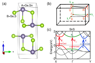
Recognized as one type of valleytronic materials, 2-dimensional (2D) group-IV monochalcogenids AB (A=Ge,Sn;B=Se,S) have received extensive attentions AB_monogap ; AB_monomemory ; AB_monopolarization ; AB_nanoletter ; DS_3 ; DS_4 ; DS_5 ; gese1 ; gese2 ; gese3 ; gese4 ; gese5 . Experimentally, group-IV monochalcogenids adopt an orthorhombic structure ( space group) as shown in Fig. 1(a), where one unit cell is constructed by two puckered polar layers similar to that of black phosphorus blackP_absorb1 ; blackP_absorb2 ; blackP_absorb3 . So monochalcogenids can be exfoliated to the monolayer AB_monomemory ; exfoliate_1 , and feature multiple valleys MultiValley1 , distinctive optical selection rules OpticalSelection1 ; OpticalSelection2 , extraordinary spintronics spintronics , large piezoelectric piezoelectric and ferroelectric effects ferroelectric_1 ; DV_2 ; DV_3 .
While valleytronics are widely studied in the 2D materials, the valley physics and their polarization generating in 3-dimensional (3D) compounds is rarely achieved. In this paper, by means of the density functional theory (DFT) calculations and symmetry analysis, we demonstrate that three pairs of valleys exist at the Fermi level in the bulk of group-IV monochalcogenids, which feature different selection rules to the linearly-polarized light. The linear polarization-resolved infrared (IR) transmission spectra are measured on the GeSe crystal. An obvious two-fold linear dichroism absorption between 8600 to 10000 is observed, corresponding to our calculations and optical absorption analyses very well. Such observation demonstrates that the valley polarization is successfully generated in the 3D group-IV monochalcogenids. Furthermore, the valley position versus the in-plane strain is also studied in this work, which offers a useful method to optimize the valleytronic properties in AB compounds. All these results provide us a new direction for the exploring of the valley materials, as well as a great guidance for the design of the photodetector and valleytonic devices.
II DFT calculations and band analysis
Our DFT calculations are performed by Vienna ab initio Simulation Package (VASP) within the projector augmented wave scheme CAL_VASP , where the generalized gradient approximation (GGA) of the Perdew-Burke-Ernzerhof type for the exchange-correlation potential DV_1 ; CAL_PBE are adopted. The cutoff energy for the wave function expansion is set to 520 eV. A Monkhorst-Pack grid of 10104 k-meshes are used for the self-consistent calculationsCAL_KPOINTS . Since the spin-orbital coupling (SOC) has very weak influence on the band structures for the existence of the inversion symmetry, we have excluded SOC in all calculations, as well as our optical selection rule analyses.
| () | () | () | A1 | B1 | |
|---|---|---|---|---|---|
| GeSe | 4.45 | 3.85 | 10.76 | (0.10,0.25,0.87) | (0.49,0.25,0.15) |
| GeS | 4.43 | 3.65 | 10.43 | (0.12,0.25,0.87) | (0.50,0.25,0.15) |
| SnSe | 4.46 | 4.19 | 11.58 | (0.12,0.25,0.87) | (0.50,0.25,0.15) |
| SnS | 4.33 | 3.98 | 11.18 | (0.12,0.25,0.87) | (0.48,0.25,0.15) |
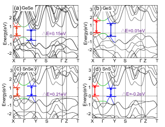
Experimental crystal parameters shown in Table I are used in our calculations. The calculated band structures of AB compounds are plotted in Fig. 2, which indicate that four AB compounds are all insulators, and have very similar band dispersions and orbital characters around the Fermi level. Therefore, we would like to take the bands of SnS as a representative to demonstrate their orbital components and valley definitions in the following. Firstly, the insulating gap for all compounds are determined by the band dispersions in the plane of the Brillouin zone (BZ), as shown in the Fig. 2. Especially, there are three energy-adjacent minima (maxima) located on the conduction (valence) band along the directions, forming three pairs of valleys, confined in direction, confined in direction, and located around point, respectively. The energy difference between and is defined as . Secondly, due to the symmetry requirement, , , and consist of different orbits and belong to different representations. As shown in Fig. 1(c) and Fig. 2, valleys colored by red and valleys colored by blue are composed of and orbitals respectively due to the existence of rotation perpendicular to the plane, while valleys represented by the green bands, are mainly composed of orbitals. The different band compositions would lead to distinctive optical absorption rules, which are summarized in Fig. 1(c), and will be analyzed in the next chapter.
III Optical selection rules
As we all know, the interband transition probability is proportional to valley_device_5 , where is the direction of the electric field of the polarized light, and are the conduction and valence band’s wave functions at a given momentum , respectively. The electron excitation from the valence band to the conduction band could happen only when the integral of is nonzero. It means that the product of , and should be unchanged under any symmetry operations of the system, i.e. their irreducible representations’ (irreps) product must be identical ( in Table II and in Table III).
Let us first address the selection rule of the valley located around the point, , which has never been studied before. According to our DFT calculations, the composition of the highest valence band and the lowest conduction band around the point are both orbitals, and their irreps are and with respect to the little group, as shown in Table II. It means that only the irrep satisfies , i.e., only the -polarized light could excite the electrons transition between the valleys. For the and valleys, their little group are both . Two valleys (red bands in Fig. 1 and Fig. 2) located along direction both belong to irrep, which decides that only the -polarized light with irrep could excite the polarization, yielding to the requirement . On the other hand, two valleys located along direction both have irreps. Thus, only the -polarized light could excite the polarization due to . The optical absorption rules of , and are summarized in Fig. 1(c). Using these features, we can distinguish the direct energy gaps of and valleys. We note that the energy gap between the valleys, i.e. , is always larger than that between valleys () based on our calculations. So we can identify by observing the absorption edge of the -polarized light. Furthermore, two kinds of valley polarization can be generated, since and can be pumped separately by applying the -polarized light.
IV Valley polarization generation
Guiding by the above analysis, we have grown GeSe and GeS compounds, and measured the linearly-polarized IR transmission spectra to verify the the polarization-dependent absorption (linear dichroism), as well as the generation of the valley polarization in the 3D group-IV monochalcogenids. Here we take GeSe as an example to illustrate such linear dichroism and the valley polarization generation.
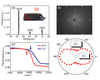
Our GeSe crystals are grown by the chemical vapor transport(CVT) technique with iodine as the transporting agent CVT_1 ; CVT_2 . High purity germanium () and selenium () powders with 1:1 composition are thoroughly mixed and sealed together with iodine (4 mg/liter) in a silica ampule under pressure of Pa. The sealed ampule is placed into a two stage horizontal furnace. The hot end with the mixture is slowly heated to 820 K at the rate of 35 K/h and the cold end to 770 K at the rate of 32 K/h. The slow heating rate is necessary to avoid any explosion due to the strong exothermic reaction between the elements. After 120 hours of growth, the furnace is cooled down naturally. Single crystals of GeSe with the size of are obtained after breaking the quartz ampoule, as shown in the inset of Fig.3(a).
| function | |||||||||
|---|---|---|---|---|---|---|---|---|---|
| 1 | 1 | 1 | 1 | 1 | 1 | 1 | 1 | 1 | |
| 1 | -1 | 1 | -1 | 1 | -1 | 1 | -1 | ||
| 1 | 1 | -1 | -1 | -1 | -1 | 1 | 1 | ||
| 1 | -1 | -1 | 1 | -1 | 1 | 1 | -1 |
| function_ | function_ | |||||
|---|---|---|---|---|---|---|
| 1 | 1 | 1 | 1 | 1 | 1 | |
| 1 | -1 | -1 | 1 | |||
| 1 | -1 | 1 | -1 | |||
| 1 | 1 | -1 | -1 |
The as-grown crystals are characterized by the scanning electron microscopy (SEM) with energy dispersive spectrometer (EDS), single crystal X-ray diffraction (XRD) and Laue back reflection measurements. Stoichiometric GeSe composition is confirmed by the EDS analysis. The flat surface is identified to be (0 0 1) plane by the single crystal XRD measurements, as displayed in Fig.3(a). It indicates that the flat surface is perpendicular to the crystalline -axis (defined as -direction), therefore it is the ab-plane in the structure XRD ; XRD_2 . The - and -axis (- and -direction) in this surface are determined by Laue back reflection camera system Lauebackreflectioncamera , which is shown in Fig.3(b).
The linear polarization-resolved IR transmission spectra of GeSe crystals are measured at room temperature using a Bruker IFS 80v spectrometer. The incident beam is along the direction and the linearly-polarized electric field could be turned within the -plane. Fig.3(c) shows the transmission spectra with electric field along the - and -direction, respectively. The sharp drop signals the onset of the absorption due to that the photon energy exceeds the band gap, which can be used to identify the value of the direct valley energy gap, and . The measurements demonstrate a clear linear dichroism between 8600 to 10000 . For the -polarized light, the onset of absorption is about 8600 (or 1.07 eV), corresponding to our calculated eV. By contrast, the onset absorption of the -polarized light is enhanced to about 9100 (or 1.13 eV), corresponding to our calculated eV roughly. The observed difference of and is 0.06 eV, a little smaller than our calculated result 0.15eV, but declaring the existence of the linear dichroism absorption enough. To further resolve the linear dichroism, we measured the polarization-dependent IR transmission spectra of the same sample with the normal light incidence and the polarization angles relative to -direction from to in steps of . Fig.3(d) shows the measured band gaps in a polar coordinate. A two-fold anisotropy along the and directions could be clearly seen in the plot, reflecting the electronic anisotropy along the and directions.
The observed linear dichroism in GeSe perfectly confirm our DFT calculations and the optical absorption analyses. More importantly, it also demonstrates that the valley polarization has been successfully generated by the linearly-polarized light in group-IV monochalcogenids, which is realized in a 3D system for the first time. Such valley polarization can be detected by the converse process, or by using the nonlinear transverse valley conductivity. Therefore our results provide new functionalities in optical switches and valleytonics devices of the 3D group-IV monochalcogenids.
V Valley modulation
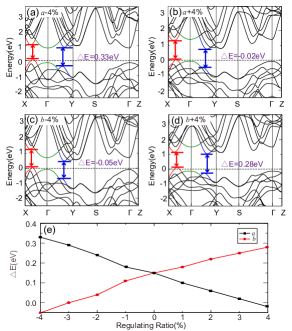
To enhance the performance of the optical switches and the valley polarization, one expects that the energy difference should be as large as possible, and the valleys should be away from the Fermi level as far as they can. Based on our calculations, SnS satisfies these requirements mostly, which is the best 3D valley material among group-IV monochalcogenides. On the other hand, we can modify the valley position by modulating the external conditions, such as strain ModulationStrain1 ; ModulationStrain2 , gating field ModulationGatingfield1 ; ModulationGatingfield2 et al. Since and are decided by the energy positions of the and orbitals. One would naturally expect that the in-plane strains are one of the effective methods to modulate . In Fig.4 (a-d), we have plotted the band structures of GeSe by reducing or enlarging of -axis and -axis respectively, which confirms that reducing a-axis or enlarging -axis can both support a larger linear dichroism energy window, i.e. a larger . The evolution of the -axis (-axis) stain is summarized in Fig. 4(e), from which we can see that either reducing constant or enlarging constant could increase the monotonically. However, for the case of reducing -axis, those valleys become very close to the Fermi level as shown in Fig. 4(a), which is disadvantageous to the polarization with the pure -direction momentum. Therefore, we conclude that enlarging -axis is the ideal way to get the best valleytronic properties in GeSe.
VI Conclusions
Combining the DFT calculations and the linear polarization-resolved IR transmission measurement together, we have proposed a family of 3D valleytronic materials AB (A=Ge, Sn; B=S,Se), in which a distinctive two-fold anisotropic absorption of the linearly-polarized light is observed, consistent with the optical absorption rule analyses very well. The observed linear dichroism perfectly confirmed that valley polarization is successfully generated by the linearly-polarized light in a 3D system. Such valley polarization can be read by using the nonlinear transverse valley conductivity. Furthermore, valley modulation by the in-plane strain is also studied in our work, which points out a useful method to optimize the vallaytronic properties in AB compounds. All these results open a new direction for the exploration of the valley materials, which also provide a good platform of optical switches and valleytonic devices.
Thank Zhida Song for useful discussion. This work is supported by the National Thousand-Young-Talents Program and the NSFC. S.-J. Z and N.-L. W are supported by supported by the National Science Foundation of China (No. 11327806), the National Key Research and Development Program of China (No.2016YFA0300902).
References
- [1] JL Garcia-Pomar, A Cortijo, and M Nieto-Vesperinas. Fully valley-polarized electron beams in graphene. Physical review letters, 100(23):236801, 2008.
- [2] Di Xiao, Gui-Bin Liu, Wanxiang Feng, Xiaodong Xu, and Wang Yao. Coupled spin and valley physics in monolayers of MoS2 and other group-VI dichalcogenides. Physical Review Letters, 108(19):196802, 2012.
- [3] Kamran Behnia. Condensed-matter physics: polarized light boosts valleytronics. Nature nanotechnology, 7(8):488–489, 2012.
- [4] Christoph E Nebel. Valleytronics: Electrons dance in diamond. Nature materials, 12(8):690–691, 2013.
- [5] Hualing Zeng, Junfeng Dai, Wang Yao, Di Xiao, and Xiaodong Cui. Valley polarization in MoS2 monolayers by optical pumping. Nature nanotechnology, 7(8):490–493, 2012.
- [6] Kin Fai Mak, Keliang He, Jie Shan, and Tony F Heinz. Control of valley polarization in monolayer MoS2 by optical helicity. Nature nanotechnology, 7(8):494–498, 2012.
- [7] Kamran Behnia. Condensed-matter physics: polarized light boosts valleytronics. Nature nanotechnology, 7(8):488–489, 2012.
- [8] Ajit Srivastava, Meinrad Sidler, Adrien V Allain, Dominik S Lembke, Andras Kis, and A Imamoğlu. Valley zeeman effect in elementary optical excitations of monolayer WSe2. Nature Physics, 2015.
- [9] Yilei Li. Valley splitting and polarization by zeeman effect in monolayer MoSe2. In Probing the Response of Two-Dimensional Crystals by Optical Spectroscopy, pages 55–64. Springer, 2016.
- [10] Honglai Li, Xidong Duan, Xueping Wu, Xiujuan Zhuang, Hong Zhou, Qinglin Zhang, Xiaoli Zhu, Wei Hu, Pinyun Ren, Pengfei Guo, et al. Growth of alloy MoS2xSe2(1-x) nanosheets with fully tunable chemical compositions and optical properties. Journal of the American Chemical Society, 136(10):3756–3759, 2014.
- [11] Qing Hua Wang, Kourosh Kalantar-Zadeh, Andras Kis, Jonathan N Coleman, and Michael S Strano. Electronics and optoelectronics of two-dimensional transition metal dichalcogenides. Nature nanotechnology, 7(11):699–712, 2012.
- [12] Qing Hua Wang, Kourosh Kalantar-Zadeh, Andras Kis, Jonathan N Coleman, and Michael S Strano. Electronics and optoelectronics of two-dimensional transition metal dichalcogenides. Nature nanotechnology, 7(11):699–712, 2012.
- [13] Priya Johari and Vivek B Shenoy. Tuning the electronic properties of semiconducting transition metal dichalcogenides by applying mechanical strains. ACS nano, 6(6):5449–5456, 2012.
- [14] Manish Chhowalla, Hyeon Suk Shin, Goki Eda, Lain-Jong Li, Kian Ping Loh, and Hua Zhang. The chemistry of two-dimensional layered transition metal dichalcogenide nanosheets. Nature chemistry, 5(4):263–275, 2013.
- [15] Hualing Zeng, Junfeng Dai, Wang Yao, Di Xiao, and Xiaodong Cui. Valley polarization in MoS2 monolayers by optical pumping. Nature nanotechnology, 7(8):490–493, 2012.
- [16] Di Xiao, Gui-Bin Liu, Wanxiang Feng, Xiaodong Xu, and Wang Yao. Coupled spin and valley physics in monolayers of MoS2 and other group-VI dichalcogenides. Physical Review Letters, 108(19):196802, 2012.
- [17] Lídia C Gomes and A Carvalho. Phosphorene analogues: Isoelectronic two-dimensional group-IV monochalcogenides with orthorhombic structure. Physical Review B, 92(8):085406, 2015.
- [18] Paul Z Hanakata, Alexandra Carvalho, David K Campbell, and Harold S Park. Memory effects in monolayer group-IV monochalcogenides. Stress (GPa), 1(1.5):2, 2016.
- [19] Paul Z Hanakata, Alexandra Carvalho, David K Campbell, and Harold S Park. Polarization and valley switching in monolayer group-IV monochalcogenides. Physical Review B, 94(3):035304, 2016.
- [20] Guangsha Shi and Emmanouil Kioupakis. Anisotropic spin transport and strong visible-light absorbance in few-layer SnSe and GeSe. Nano letters, 15(10):6926–6931, 2015.
- [21] Lijun Zhang and D. J. Singh. Electronic structure and thermoelectric properties of layered materials. Phys. Rev. B, 80:075117, Aug 2009.
- [22] David Parker and David J. Singh. High temperature thermoelectric properties of rock-salt structure PbS. Solid State Communications, 182:34 – 37, 2014.
- [23] David Parker and David J Singh. First principles investigations of the thermoelectric behavior of tin sulfide. Journal of Applied Physics, 108(8):083712, 2010.
- [24] Rangel, Tonatiuh and Fregoso, Benjamin M. and Mendoza, Bernardo S. and Morimoto, Takahiro and Moore, Joel E. and Neaton, Jeffrey B.. Large Bulk Photovoltaic Effect and Spontaneous Polarization of Single-Layer Monochalcogenides. Phys. Rev. Lett., 119(6):067402, 2017
- [25] Bertrand, Simon and Garate, Ion and Côté, René. Light-induced valley polarization in interacting and nonlinear Weyl semimetals. Phys. Rev. B, 96(7):075126, 2017
- [26] Bertrand, S. and Garate, I. and Côté, R.. Optical absorption in interacting and nonlinear Weyl semimetals. arXiv, 1704.08939, 2017
- [27] Pletikosić, I. and von Rohr, F. and Pervan, P. and Das, P. K. and Vobornik, I. and Cava, R. J. and Valla, T.. Band structure of a IV-VI black phosphorus analogue, the thermoelectric SnSe. arXiv, 1707.04289,2017
- [28] von Rohr, Fabian O. and Ji, Huiwen and Cevallos, F. Alexandre and Gao, Tong and Ong, N. Phuan and Cava, Robert J.. High-Pressure Synthesis and Characterization of -GeSe A Six-Membered-Ring Semiconductor in an Uncommon Boat Conformation. Journal of the American Chemical Society, 139(7):2771-2777,2017
- [29] Likai Li, Yijun Yu, Guo Jun Ye, Qingqin Ge, Xuedong Ou, Hua Wu, Donglai Feng, Xian Hui Chen, and Yuanbo Zhang. Black phosphorus field-effect transistors. Nature nanotechnology, 9(5):372–377, 2014.
- [30] Fengnian Xia, Han Wang, and Yichen Jia. Rediscovering black phosphorus as an anisotropic layered material for optoelectronics and electronics. Nature communications, 5, 2014.
- [31] Jingsi Qiao, Xianghua Kong, Zhi-Xin Hu, Feng Yang, and Wei Ji. High-mobility transport anisotropy and linear dichroism in few-layer black phosphorus. Nature communications, 5, 2014.
- [32] Jack R Brent, David J Lewis, Tommy Lorenz, Edward A Lewis, Nicky Savjani, Sarah J Haigh, Gotthard Seifert, Brian Derby, and Paul O Brien. Tin (ii) sulfide(SnS) nanosheets by liquid-phase exfoliation of herzenbergite: IV-VI main group two-dimensional atomic crystals. Journal of the American Chemical Society, 137(39):12689–12696, 2015.
- [33] S. Gwo, K.-J. Chao, C. K. Shih, K. Sadra, and B. G. Streetman. Direct mapping of electronic structure across As/GaAs heterojunctions: Band offsets, asymmetrical transition widths, and multiple-valley band structures. Phys. Rev. Lett., 71:1883–1886, Sep 1993.
- [34] Yu-xi Liu, J. Q. You, L. F. Wei, C. P. Sun, and Franco Nori. Optical selection rules and phase-dependent adiabatic state control in a superconducting quantum circuit. Phys. Rev. Lett., 95:087001, Aug 2005.
- [35] P. Voisin, G. Bastard, and M. Voos. Optical selection rules in superlattices in the envelope-function approximation. Phys. Rev. B, 29:935–941, Jan 1984.
- [36] David D Awschalom and Michael E Flatté. Challenges for semiconductor spintronics. Nature Physics, 3(3):153–159, 2007.
- [37] Wanling Pan and Farrokh Ayazi. Thin-film piezoelectric-on-substrate resonators with Q enhancement and TCF reduction. In Micro Electro Mechanical Systems (MEMS), 2010 IEEE 23rd International Conference on, pages 727–730. IEEE, 2010.
- [38] Guo-Xing Miao and Jagadeesh S Moodera. Spin manipulation with magnetic semiconductor barriers. Physical Chemistry Chemical Physics, 17(2):751–761, 2015.
- [39] R. D. King-Smith and David Vanderbilt. Theory of polarization of crystalline solids. Phys. Rev. B, 47:1651–1654, Jan 1993.
- [40] Fabio Bernardini, Vincenzo Fiorentini, and David Vanderbilt. Polarization-based calculation of the dielectric tensor of polar crystals. Phys. Rev. Lett., 79:3958–3961, Nov 1997.
- [41] G Kresse, J. Furthmüller. Software VASP, Vienna, 1999.
- [42] David Vanderbilt. Soft self-consistent pseudopotentials in a generalized eigenvalue formalism. Phys. Rev. B, 41:7892–7895, Apr 1990.
- [43] Matthias Ernzerhof and Gustavo E Scuseria. Assessment of the Perdew–Burke–Ernzerhof exchange-correlation functional. The Journal of chemical physics, 110(11):5029–5036, 1999.
- [44] Hendrik J Monkhorst and James D Pack. Special points for brillouin-zone integrations. Physical review B, 13(12):5188, 1976.
- [45] Heribert Wiedemeier, Eugene A Irene, and Asim K Chaudhuri. Crystal growth by vapor transport of GeSe, GeSe2, and GeTe and transport mechanism and morphology of GeTe. Journal of Crystal Growth, 13:393 – 396, 1972.
- [46] Atsushi Okazaki. The crystal structure of germanium selenide GeSe. Journal of the Physical Society of Japan, 13(10):1151–1155, 1958.
- [47] Ajay Agarwal, P. D. Patel, and D. Lakshminarayana. Single crystal growth of layered tin monoselenide semiconductor using a direct vapour transport technique. Journal of Crystal Growth, 142(142):344–348, 1994.
- [48] R. Nitsche, H. U. Blsterli, and M. Lichtensteiger. Crystal growth by chemical transport reactions i : Binary, ternary, and mixed-crystal chalcogenides. Journal of Physics Chemistry of Solids, 21(s 3 C4):199 C205, 1961.
- [49] HC Hsueh, H Vass, SJ Clark, GJ Ackland, and J Crain. High-pressure effects in the layered semiconductor germanium selenide. Physical Review B, 51(23):16750, 1995.
- [50] E. D. Minot, Yuval Yaish, Vera Sazonova, Ji-Yong Park, Markus Brink, and Paul L. McEuen. Tuning carbon nanotube band gaps with strain. Phys. Rev. Lett., 90:156401, Apr 2003.
- [51] Liangzhi Kou, Thomas Frauenheim, and Changfeng Chen. Nanoscale multilayer transition-metal dichalcogenide heterostructures: Band gap modulation by interfacial strain and spontaneous polarization. The Journal of Physical Chemistry Letters, 4(10):1730–1736, 2013. PMID: 26282986.
- [52] A. V. Malyshev. DNA double helices for single molecule electronics. Phys. Rev. Lett., 98:096801, Feb 2007.
- [53] S. Caprara, F. Peronaci, and M. Grilli. Intrinsic instability of electronic interfaces with strong rashba coupling. Phys. Rev. Lett., 109:196401, Nov 2012.