Superconducting Caps for Quantum Integrated Circuits
Abstract
We report on the fabrication and metrology of superconducting caps for qubit circuits. As part of a 3D quantum integrated circuit architecture, a cap chip forms the upper half of an enclosure that provides isolation, increases vacuum participation ratio, and improves performance of individual resonant elements. Here, we demonstrate that such caps can be reliably fabricated, placed on a circuit chip, and form superconducting connections to the circuit.
I Motivation
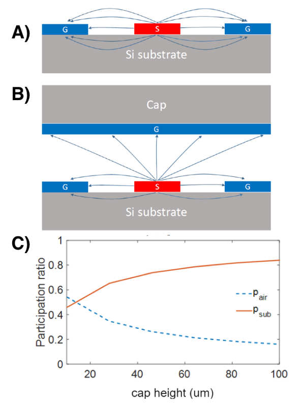
Superconducting qubits are highly sensitive detectors of material quality. The coupling of qubits’ electromagnetic modes with lossy, defective materials can limit their coherence time. In a 2D circuit geometry the field lines are largely in the plane, as in Fig. 1A, where the mode interacts strongly with interface and substrate defects. One way to avoid this is to place qubits inside a 3D cavity, which increases the modes’ participation in lossless vacuum, thereby reducing microwave loss and increasing qubit lifetime 3Dtransmon . However, this approach sacrifices the scalability and density of 2D circuits.
To confer some benefits 3D cavities onto a 2D circuit, we propose a geometry as illustrated in Fig. 1B in which a superconducting cap is placed on top of the chip. Here, field lines terminate preferentially on the walls of the enclosure, which increases the spatial overlap of the mode with the lossless medium of free space. Microwave simulations of superconducting resonators underneath a cap, as in Fig. 1C., indicate a strong response of the electromagnetic vacuum participation ratio to the cap height.
In addition, when employing a non-planar quantum integrated circuit architecture including superconducting vias, we can engineer separate shielded enclosures to improve the electromagnetic isolation and reduce crosstalk between circuit elements. Simulations indicate that such enclosures reduce crosstalk between neighboring resonant elements by 15 dB.
In summary, we expect that bonding caps with a superconducting liner over qubit circuits will confer improved coherence times, reduced crosstalk, and better immunity to environmental noise.
II Fabrication
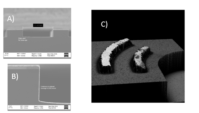
The cap is composed of pockets etched in Si, coated with superconducting metal, and patterned with indium bumps as a superconducting adhesive for bonding to the circuit chip. Caps are fabricated from silicon-on-insulator wafers, in which a 24 m Si device layer is sandwiched on both sides by 1 m of oxide, with thick Si underneath for structural support. The top side of the wafer is patterned with photoresist, first to mask an inductively coupled plasma etch that selectively removes the top oxide (Fig. 2A) to pattern bumps that limit the gap between cap and circuit, and then a second time to mask a deep reactive ion etch (DRIE) down to the buried oxide. The DRIE follows the Bosch process bosch , producing a square pocket with vertical sidewalls 24 m deep (Fig. 2B). The DRIE step employs a LF substrate bias to avoid footing near the buried oxide. The surface is then conformally coated with 1 m sputtered Al to form a continuous superconducting shield. The resulting profile is visualized in Fig. 3A and Fig. 3B, confirming a continuous sputtered film and smooth, vertical sidewalls from the Bosch process.
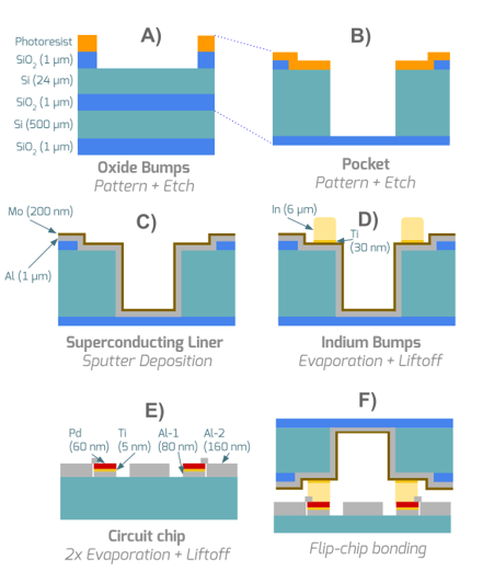
In order to form high quality interfaces, the terminating metal layers on the cap and circuit (which will mediate the indium connection) are selected to avoid or mitigate native oxides. On the cap side, termination with an Al native oxide is avoided by capping the Al in-situ (without breaking vacuum) with a thin, 200 nm Mo film (Fig. 2C). Mo is a refractory metal that is superconducting near 1 K. Similarly, Pd is chosen to terminate bond pads on the circuit side. Although Pd is not superconducting at our operating temperature, it is designed to be thin enough to still behave as a superconductor through the proximity effect.
To form this electrical and mechanical connection between circuit and cap, evaporated indium bumps (with Ti adhesion layers) are patterned on the cap. Electrically, indium serves as an ideal Type-I superconducting bond to ground the cap, as it has a above 3 K. Several groups have successfully used superconducting indium bumps to bond chips with qubits to another chip with readout and control signals with high qubit coherence (20 s) lincoln ; google ; google2 , which is a more technically demanding application. Electron-beam evaporation is chosen for indium deposition, since it is well known to produce high quality indium films, and is amenable for liftoff (Fig. 2D). The patterned bumps are found to be well defined, as seen in the confocal microscope image of Fig. 3C.
The circuit chip is produced in two liftoff steps. First, we pattern bond pads for contacting the indium, deposit 85 nm Al, 5 nm Ti, and 60 nm Pd, then perform liftoff. The palladium is a noble metal that does not oxidize, and is commonly used for bonding purposes. Although it does not superconduct, it will experience the superconducting proximity effect by being sandwiched between Al and In. It is in this way possible to form a continuous superconducting path from the circuit to cap chip despite the use of normal metals, albeit it with a weak link, so long as those normal layers are thin enough. The second step of the circuit chip fabrication is to pattern, deposit, and liftoff superconducting circuit features (ground plane, resonators, etc.) with 160 nm of Al, allowing for some overlap on the bonding pads to ensure a good electrical connection (Fig. 2E). This is performed in a Plassys e-beam evaporation system, designed for Josephson Junction (JJ) fabrication.
To form the 3D structure, we use a flip-chip bonder to affix the cap chip to the circuit chip (Fig. 2F). The two chips are precisely aligned and pressed together under up to 45 kg of weight at around 70∘ C. Note that the 1 m oxide bumps are patterned to place a limit on how close the cap and circuit chip come in contact during bonding. Though in practice, we do not need to apply the required force to press the indium flush with the oxide bumps.
III Test structures
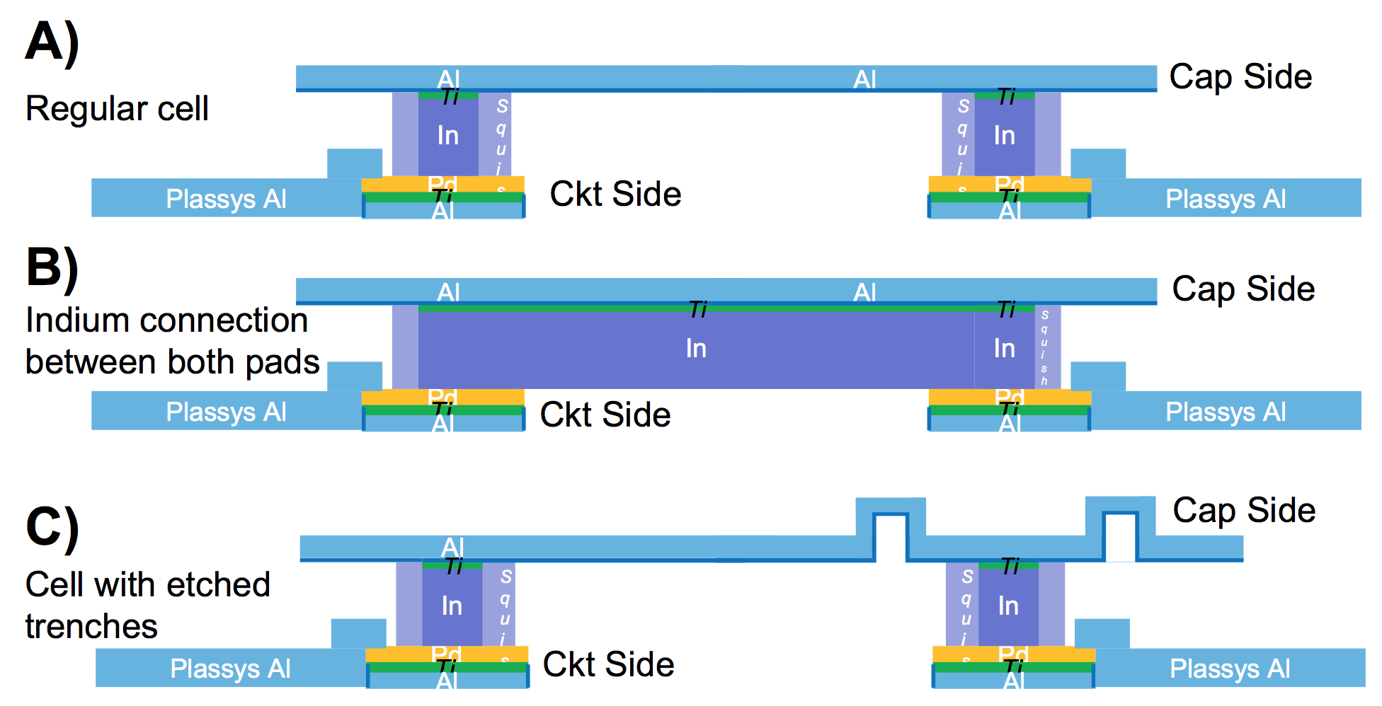
To assess the quality of the bond across the die, test structures shown in Fig. 4 were designed to measure series resistance across indium bumps. The conductive path is designed such that current must traverse from the circuit metal to the cap through an indium bump, then back to the circuit along an adjacent indium bump. Some special test structures were also implemented, to test the conformality of the sputtered Al, and others to test the intrinsic contact resistance between indium and palladium. To test for Al conformality, trenches with the same depth as the pocket are etched into the cap between adjacent indium bumps. If the Al layer is not continuous, current injected through one bump is not able to find a return path to the circuit. To test the contact resistance of just the indium-palladium interface, two adjacent pads are shorted with indium, such that current does not need to flow through the cap for continuity.
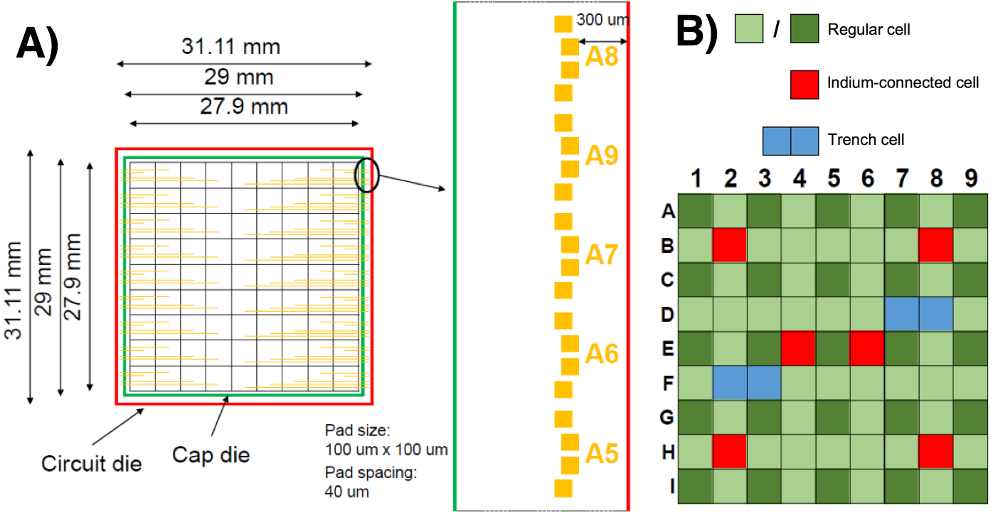
The test structures were fabricated on a 31 mm circuit chip and a corresponding 29 mm cap chip, arranged in a grid with signal lines designed so that all 81 structures could be measured from the circuit chip edges (Fig. 5A). This arrangement allows us to probe sites distributed across a large chip and test planarity of the bond. Most of the test structures were standard cells, with 6 In-connected cells and 4 with trenches (Fig. 5B).
IV Results
At room temperature, series resistances below 5 were obtained at 80 out of 81 test sites, demonstrating excellent continuity and high process fidelity. From the lowest resistance values measured, the room temperature contact resistance between indium and molybdenum is less than 0.2 . No difference was measured between the different test structure types, indicating that the Al layer is indeed continuous across the pockets. Furthermore no major asymmetries in resistance were observed between the left and right sides or top and bottom of the chip, indicating that bond parallelism across a large 31 mm chip is acceptable.
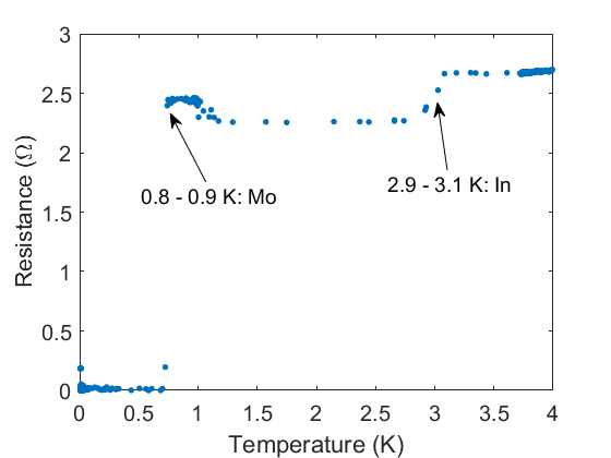
We also performed cryogenic measurements to assess the superconducting properties. An example is shown in Fig. 6. As we cool the sample down, we see sharp resistance drops at 2.9-3.1 K and 0.8-0.9 K, which correspond approximately to the superconducting transition temperatures of In and Mo/Al, respectively. The absence of separate Al and Mo transitions could be explained by a variety of superconducting-normal interface effects.
In any case, under 0.8 K we observe zero resistance, below the sensitivity of our instruments, indicative of a superconducting path from the circuit chip to the cap chip and back. Our instruments set the lower bound of the critical current of this path as 36 A.
V Conclusions
The application of a Mo capping layer to the Al cap has proven to be an effective means of mitigating the deleterious effects of native oxide on the electrical and mechanical contact of indium bumps between circuit and cap die. In addition, the consistently low room-temperature resistances and clear low-temperature superconductivity demonstrate that the cap can be kept grounded by robust supercurrents through the bonds, at locations across the die.
With successful basic metrology of this technology established, we can move onto integration with superconducting quantum circuits, including qubits. Further work is needed to systematically establish enhancements to qubit performance.
References
- (1) Hanhee Paik, et al., Observation of High Coherence in Josephson Junction Qubits Measured in a Three-Dimensional Circuit QED Architecture, Phys. Rev. Lett. 107, 240501 (2011).
- (2) F. Marty, L. Rousseau, B. Saadany, B. Mercier, O. Francais, Y. Mita, T. Bourouina, Advanced etching of silicon based on deep reactive ion etching for silicon high aspect ratio microstructures and three-dimensional micro- and nanostructures, Microelectronics Journal 36, 7 (2005).
- (3) D. Rosenberg, et al., 3D integrated superconducting qubits, arXiv:1706.04116 (2017).
- (4) M. Mohseni, et. al., Commercialize quantum technologies in five years, Nature 543, 7644 (2017).
- (5) J. Mutus, et. al., H46.00006: 3D integration of superconducting qubits with bump bonds: Part 1, J. Kelly, et. al., H46.00007: 3D integration of superconducting qubits with bump bonds: Part 2, E. Lucero, et. al., H46.00008: 3D integration of superconducting qubits with bump bonds: Part 3, APS March Meeting 2017