Electronic structure of charged bilayer and trilayer phosphorene
Abstract
We have investigated the electronic structure of charged bilayer and trilayer phoshporene using first-principles, density-functional-theory calculations. We find that the effective dielectric constant for an external electric field applied perpendicular to phosphorene layers increases with the charge density and is twice as large as in an undoped system if the electron density is around cm-2. It is known that if few-layer phosphorene is placed under such an electric field, the electron band gap decreases and if the strength of the electric field is further increased, the band gap closes. We show that the electronic screening due to added charge carriers reduces the amount of this reduction in the band gap and increases the critical strength of the electric field for gap closure. If the electron density is around cm-2, for example, this critical field for trilayer phosphorene is 40 % higher than that for a charge-neutral system. The results are directly relevant to experiments on few-layer phosphorene with top and bottom electrical gates and / or with chemical dopants.
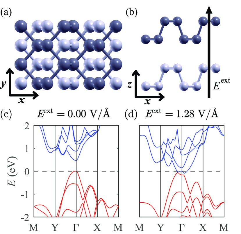
Phosphorene, a single-layer of black phosphorus, has recently been isolated by mechanical exfoliation Li et al. (2014); Koenig et al. (2014); Liu et al. (2014). Among many exfoliated two-dimensional materials, phosphorene is unique in that due to its structural anisotropy [Fig. 1(a)] the thermal and electrical transport Liu et al. (2014); Fei and Yang (2014), critical strains Wei and Peng (2014) and Young’s moduli Wang et al. (2015); Jiang and Park (2014) along the two in-plane directions [ and in Fig. 1(a)] are different.
The electronic structure of few-layer phosphorene has been tuned by chemical doping that effectively acts as an electric field along the surface-normal direction and at the same time as additional charge carriers Kim et al. (2015) [Fig. 1(b)]. Also, a recent experimental study shows that top and bottom electrical gating can tune the band gap of few-layer phosphorene efficiently Deng et al. (2017).
There have been several density-functional-theory studies on few-layer phosphorene since the first such studies Li et al. (2014); Koenig et al. (2014); Liu et al. (2014). Two-dimensional massless Dirac fermions are generated if few-layer phosphorene is placed under a strong enough external electric field irrespective of whether the spin-orbit coupling is taken into account or not Baik et al. (2015). How the electronic structure changes with the number of layers Kumar et al. (2016); Dolui and Quek (2015), stacking order Dai and Zeng (2014); Cakir et al. (2015), strength of an applied electric field Baik et al. (2015); Dai and Zeng (2014); Kumar et al. (2016); Liu et al. (2015); Ghosh et al. (2016); Dolui and Quek (2015) and strain Peng et al. (2014) has been extensively studied. The effects of various transition metal dopants have also been investigated Zhang et al. (2015a); Yu et al. (2015); Sui et al. (2015); Jing et al. (2015); Hu and Hong (2015). The possibility of electron-doped phosphorene being a superconductor above liquid-helium temperature was considered Shao et al. (2014).
Although there have been many such first-principles-based density-functional-theory studies on few-layer phosphorene, the joint effects on the electronic structure of an external electric field and added charge carriers while controlling the two factors independently have not been investigated so far. However, such a computational study is directly relevant to the dual-electrical-gate (top and bottom gates) experiments on few-layer phosphorene either with or without molecular dopants and to device applications based on few-layer phosphorene. (A study on bilayer graphene in this spirit was performed Gava et al. (2009).)
In this paper, the effects of doping with charge carriers on the effective dielectric constant [for a field along as shown in Fig. 1(b)] and on the field-induced band gap modulation and Lifshitz phase transitions of bilayer and trilayer phosphorene are studied from first-principles-based density-functional-theory calculations. The screening from added charge carriers reduces the net electric field at the interlayer region. This reduction in the electric field results in an increase in the effective dielectric constant. For example, if the electron density is cm-2, the effective dielectric constant is roughly twice as large as its value in undoped systems. Moreover, the band gap reduction due to an external electric field is decreased due to enhanced screening from the doped charge carriers. Hence, the strength of the critical external electric field for gap closure [Figs. 1(c) and 1(d)] is increased upon doping. For example, the critical field for trilayer phosphorene if the electron density is cm-2 is 40 % higher than that for the charge-neutral system.
Our first-principles calculations were performed with Quantum Espresso package Giannozzi et al. (2009). We used a plane-wave basis set with a kinetic-energy cutoff of 50 Ry and adopted the generalized gradient approximation of Perdew, Burke, and Ernzerhof Perdew et al. (1996) for exchange correlation energy. Core-valence interactions were modeled by Troullier-Martins norm-conserving pseudopotentials Troullier and Martins (1991). We have not considered spin-orbit interactions since the screening properties are not affected much. The Brillouin zone is sampled by a Monkhorst-Pack grid (Monkhorst and Pack, 1976). Note that such a dense sampling is necessary for convergence in the case of doped, metallic systems contrary to the case of undoped, semiconducting system.
The stable structure is obtained by fully relaxing the atomic positions until all the components of the Hellmann-Feynman force on each atom are weaker than 0.01 eV/Å. Van der Waals interactions are accounted for by using an empirical correction method Grimme (2006). This method has been proven to be effective in describing layered materials Grimme et al. (2007); Antony and Grimme (2008); Hu et al. (2014). We have checked that the atomic displacements due to extra doped charges or vertical external electric fields considered in our work are less than 0.5 % of the bond lengths (since the material is not polar). We have checked that in agreement with previous studies Zhang et al. (2015b); Cakir et al. (2015); Dai and Zeng (2014) the stable stacking order of bilayer phosphorene is of AB type such that even layers are shifted half the lattice period along with respect to the odd layers [Fig. 1(a)]. Bulk black phosphorus is also of AB type Asahina and Morita (1984). As in previous first-principles studies Baik et al. (2015); Dai and Zeng (2014); Liu et al. (2015); Ghosh et al. (2016); Dolui and Quek (2015), the band gap closes if the external electric field [Fig. 1(b)] is strong enough [Figs. 1(c) and 1(d)].
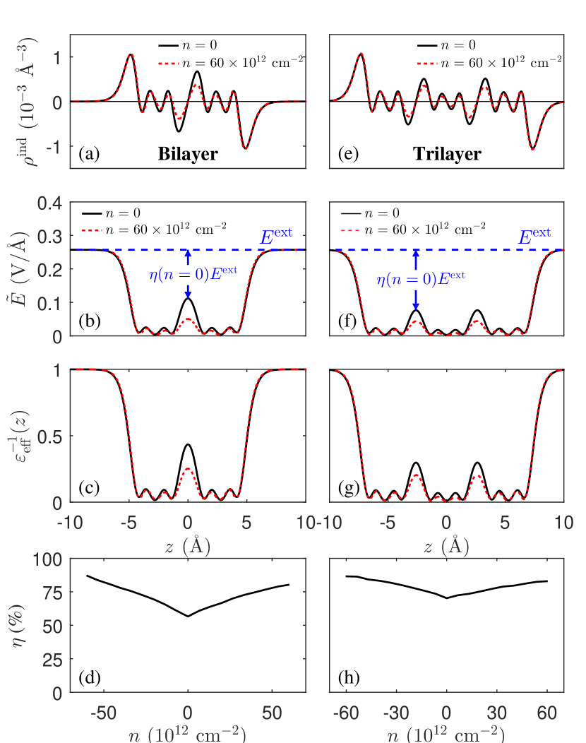
An external electric field is modeled by a saw-tooth type of potential with dipole-field correction Bengtsson (1999) and a face-to-face distance between periodic images is maintained to be 25–30 Å. The induced electron density due to an applied electric field in both doped and undoped systems is shown in Figs. 2(a) and 2(e). Note that the additional charge carriers decrease the magnitude of the field-induced charge density around the interlayer regions. This decrease naturally results in the reduction in the net, screened electric field at the interlayer regions whereas in the other parts of the material the net electric field is not reduced upon doping.
The calculated screening efficiency shown in Figs. 2(b), 2(d), 2(f) and 2(h) (also, see caption) and effective, position-dependent inverse dielectric function shown in Figs. 2(c) and 2(g) allow us to understand how the effective dielectric constant increases with the amount of doped charge carriers. In agreement with the induced charge density shown in Figs. 2(a) and 2(e), the net effect of additional charge carriers is the reduction in the net, external-field-induced electric field in the interlayer regions.
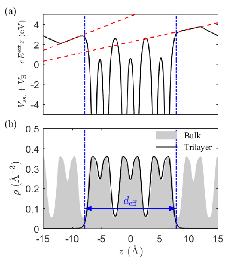
The slopes of the electrostatic potential in the two vacuum regions above and below the slab differ from each other except for undoped case. The average of the two slopes is equal to the strength of the applied external electric field. We determine the average of the screened electric field inside the material by (i) obtaining the -plane-averaged electrostatic potentials linearly extrapolated from the two vacuum regions [as illustrated by the two dashed red lines in Fig. 3(a)] at the (effective) top and bottom boundaries of the the slab (we discuss how to choose these boundaries later), (ii) taking their difference and (iii) dividing this difference by the distance between those two effective boundaries [Fig. 3(b)].
We need to define where the two effective boundaries of the material are. The natural definition of the boundaries is the positions where the -plane-averaged electron density is half the minimum value of the corresponding quantity of the bulk crystal [Fig. 3(b)]. The effective thickness defined in this way is almost the same as the bulk lattice parameter along the direction times the number of layers. The thicknesses of bilayer and trialyer phosphorene are 10.57 Å and 15.49 Å, respectively. The thicknesses per layer are 5.29 Å and 5.16 Å, respectively, close to the corresponding bulk quantity, 5.3 Å Morita (1986).
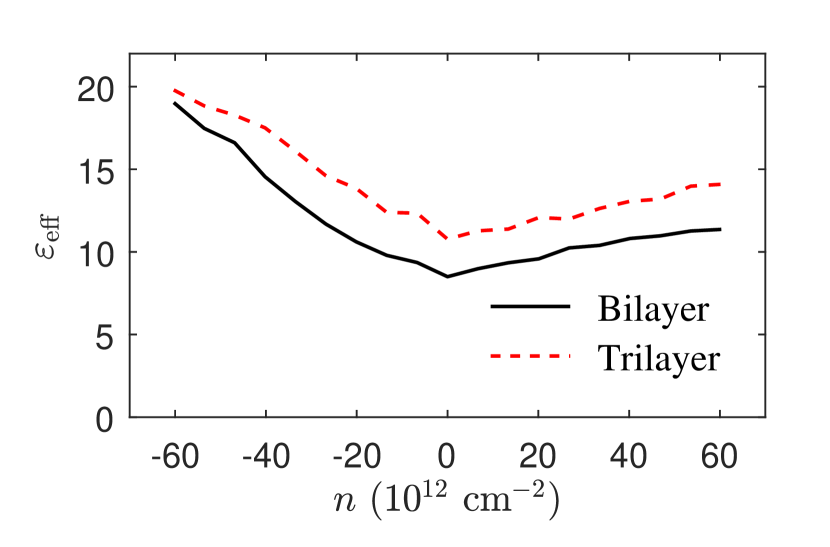
Figure 4 shows the effective dielectric constant of bilayer and trilayer phosphorene. In our calculations, we used in the linear-response regime for bilayer and trilayer phosphorene Kumar et al. (2016) (0.15 eV/Å eV/Å). N-type doping is more efficient than p-type doping in screening the external electric field and the effective dielectric constant is twice as large as in undoped systems if the electron density is around cm-2.
Calculated ’s of undoped ( in Fig. 4) bilayer and trilayer phosphorene are 8.5 and 10.8, respectively. Note that these values are much higher than those reported in Ref. Kumar et al. (2016): 2.9 for bilayer phosphorene and 3.5 for trilayer phosphorene. This discrepancy arises from the difference in the definition of the effective thickness [Fig. 3(b)]. We found that depends very sensitively on . In Ref. Kumar et al. (2016), was defined as the distance between the positions where the induced electron density [see, e. g. , Figs. 2(a) and 2(e)] drops to of the nearest peak value. The values of of bilayer and trilayer phosphorene defined in this way are 15.10 Å and 20.06 Å when eV/Å, respectively, which are longer than those in this work by 43% and 30%, respectively. Our definition of (i) does not require such an arbitrary criterion, (ii) can be defined without considering an external electric field, and (iii) will be very relevant to device applications since the effective thickness is defined based on the total electron density.
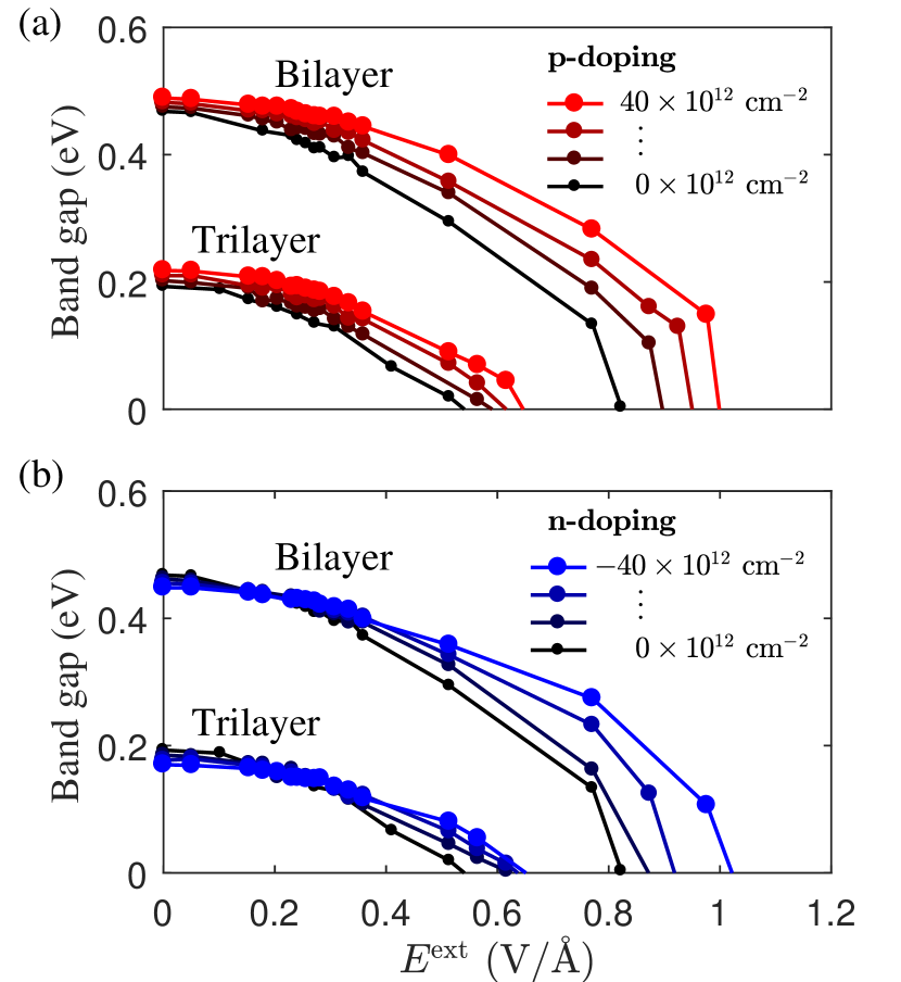
Figure 5 shows how the band gap of bilayer and trilayer phosphorene varies upon doping and applying an external electric field. If we neglect the small gap changes at zero field due to added charge carriers, the band gap decreases slower than in undoped system. Because of this behavior, the critical field strength to close the band gap of few-layer phosphorene increases with the amount of doped charge carriers (Fig. 6). For a doping with cm-2, the critical field strength for bilayer and trilayer phosphorene is increased by 20 % and 40 %, respectively.
In conclusion, we have shown that few-layer phosphorene doped with electrons or holes by external electrical gates have different electronic and screening properties than an undoped intrinsic counterpart. The effective dielectric constants can be doubled by electrical gating and the strength of the critical electric field for gap closure is significantly increased. Our work also highlights the role of additional charge carriers that can be easily introduced by electrical gates in other few-layer two-dimensional materials.
Acknowledgements.
This work was supported by the Creative-Pioneering Research Program through Seoul National University.References
- Li et al. (2014) L. Li, Y. Yu, G. J. Ye, Q. Ge, X. Ou, H. Wu, D. Feng, X. H. Chen, and Y. Zhang, Nat. Nanotech. 9, 372 (2014).
- Koenig et al. (2014) S. P. Koenig, R. A. Doganov, H. Schmidt, A. H. Castro Neto, and B. Özyilmaz, Appl. Phys. Lett. 104, 103106 (2014).
- Liu et al. (2014) H. Liu, A. T. Neal, Z. Zhu, Z. Luo, X. Xu, D. Tománek, and P. D. Ye, ACS nano 8, 4033 (2014).
- Fei and Yang (2014) R. Fei and L. Yang, Nano Lett. 14, 2884 (2014).
- Wei and Peng (2014) Q. Wei and X. Peng, Appl. Phys. Lett. 104, 251915 (2014).
- Wang et al. (2015) L. Wang, A. Kutana, X. Zou, and B. I. Yakobson, Nanoscale 7, 9746 (2015).
- Jiang and Park (2014) J.-W. Jiang and H. S. Park, J. Phys. D: Appl. Phys. 47, 385304 (2014).
- Kim et al. (2015) J. Kim, S. S. Baik, S. H. Ryu, Y. Sohn, S. Park, B.-G. Park, J. Denlinger, Y. Yi, H. J. Choi, and K. S. Kim, Science 349, 723 (2015).
- Deng et al. (2017) B. Deng, V. Tran, Y. Xie, H. Jiang, C. Li, Q. Guo, X. Wang, H. Tian, S. J. Koester, H. Wang, J. J. Cha, Q. Xia, L. Yang, and F. Xia, Nat. Comm. 8, 14474 (2017).
- Baik et al. (2015) S. S. Baik, K. S. Kim, Y. Yi, and H. J. Choi, Nano Lett. 15, 7788 (2015).
- Kumar et al. (2016) P. Kumar, B. S. Bhadoria, S. Kumar, S. Bhowmick, Y. S. Chauhan, and A. Agarwal, Phys. Rev. B 93, 195428 (2016).
- Dolui and Quek (2015) K. Dolui and S. Y. Quek, Sci. Rep. 5, 11699 (2015).
- Dai and Zeng (2014) J. Dai and X. C. Zeng, J. Phys. Chem. Lett. 5, 1289 (2014).
- Cakir et al. (2015) D. Cakir, C. Sevik, and F. M. Peeters, Phys. Rev. B 92, 165406 (2015).
- Liu et al. (2015) Q. H. Liu, X. W. Zhang, L. B. Abdalla, A. Fazzio, and A. Zunger, Nano Lett. 15, 1222 (2015).
- Ghosh et al. (2016) B. Ghosh, B. Singh, R. Prasad, and A. Agarwal, Phys. Rev. B 94, 205426 (2016).
- Peng et al. (2014) X. Peng, Q. Wei, and A. Copple, Phys. Rev. B 90, 085402 (2014).
- Zhang et al. (2015a) R. Zhang, B. Li, and J. Yang, J. Phys. Chem. C 119, 2871 (2015a).
- Yu et al. (2015) W. Yu, Z. Zhu, C.-Y. Niu, C. Li, J.-H. Cho, and Y. Jia, Phys. Chem. Chem. Phys. 17, 16351 (2015).
- Sui et al. (2015) X. Sui, C. Si, B. Shao, X. Zou, J. Wu, B.-L. Gu, and W. Duan, J. Phys. Chem. C 119, 10059 (2015).
- Jing et al. (2015) Y. Jing, Q. Tang, P. He, Z. Zhou, and P. Shen, Nanotechnology 26, 095201 (2015).
- Hu and Hong (2015) T. Hu and J. Hong, J. Phys. Chem. C 119, 8199 (2015).
- Shao et al. (2014) D. Shao, W. Lu, H. Lv, and Y. Sun, Eur. Phys. Lett. 108, 67004 (2014).
- Gava et al. (2009) P. Gava, M. Lazzeri, A. M. Saitta, and F. Mauri, Phys. Rev. B 79, 165431 (2009).
- Giannozzi et al. (2009) P. Giannozzi, S. Baroni, N. Bonini, M. Calandra, R. Car, C. Cavazzoni, D. Ceresoli, G. L. Chiarotti, M. Cococcioni, and I. Dabo, J. Phys. Condens. Matter 21, 395502 (2009).
- Perdew et al. (1996) J. P. Perdew, K. Burke, and M. Ernzerhof, Phys. Rev. Lett. 77, 3865 (1996).
- Troullier and Martins (1991) N. Troullier and J. L. Martins, Phys. Rev. B 43, 1993 (1991).
- Monkhorst and Pack (1976) H. J. Monkhorst and J. D. Pack, Phys. Rev. B 13, 5188 (1976).
- Grimme (2006) S. Grimme, J. Comput. Chem. 27, 1787 (2006).
- Grimme et al. (2007) S. Grimme, C. Mück-Lichtenfeld, and J. Antony, J. Phys. Chem. C 111, 11199 (2007).
- Antony and Grimme (2008) J. Antony and S. Grimme, Phys. Chem. Chem. Phys. 10, 2722 (2008).
- Hu et al. (2014) W. Hu, N. Xia, X. Wu, Z. Li, and J. Yang, Phys. Chem. Chem. Phys. 16, 6957 (2014).
- Zhang et al. (2015b) T. Zhang, J.-H. Lin, Y.-M. Yu, X.-R. Chen, and W.-M. Liu, Sci. Rep. 5, 13927 (2015b).
- Asahina and Morita (1984) H. Asahina and A. Morita, J. Phys. C 17, 1839 (1984).
- Bengtsson (1999) L. Bengtsson, Phys. Rev. B 59, 12301 (1999).
- Morita (1986) A. Morita, Appl. Phys. A 39, 227 (1986).