Native interstitial defects in ZnGeN2
Abstract
A density functional study is presented of the interstitial Zni, Gei, and Ni in ZnGeN2. Corrections to the band gap are included by means of the LDA+U method. The Zn and Ge interstitials are both found to strongly prefer the larger octahedral site compared to the two types of tetrahedral sites. The Zn interstitial is found to be a shallow double donor but has higher energy than previously studied antisite defects. It has a resonance in the conduction band which is Zn- like. The Ge interstitial is an even higher energy of formation defect and also behaves as a shallow double donor but has also a deep level in the gap, corresponding to a Ge- orbital character while the Ge- forms a resonance in the conduction band. The nitrogen interstitial forms a split-interstitial configuration, as also occurs in GaN. Its electronic levels can be related to that of a N2 molecule. The defect levels in the gap correspond to the -like lowest unoccupied molecular orbital (LUMO) of the molecule, which here becomes filled with 3 electrons in the defect’s neutral charge state. They are found to prefer a high-spin configuration in the state. The corresponding transition levels are obtained and show that this is an amphoteric trap level occurring in , , 0 and charge states. The two possible sites for this split interstitial, on top of Zn or on top of Ge differ slightly in N2 bond-length. While the Ni defects have the lowest formation energy among the interstitials, it is still higher than that of the antisites. Hence they are not expected to occur in sufficient concentration to affect the intrinsic Fermi level position. In particular, they do not contribute to the unintentional n-type background doping.
I Introduction
The II-IV-N2 analogs of GaN, such as ZnGeN2, ZnSnN2, Mg-IV-N2 and Cd-IV-N2 compounds have recently received considerable attention for their potential to complement the group-III nitrides as opto-electronic materials.Lambrecht and Punya (2013); Punya et al. (2011a); Quayle et al. (2015); Paudel and Lambrecht (2007); Peshek et al. (2008); Paudel and Lambrecht (2008, 2009); Punya et al. (2011b); Jaroenjittichai and Lambrecht (2016); Lyu and Lambrecht (2017); Du et al. (2008); Zhu et al. (1999) ZnSnN2 has received attention as a potential solar cell material composed entirely of earth-abundant and non-toxic elements.Feldberg et al. (2012); Lahourcade et al. (2013); Quayle et al. (2013); Fioretti et al. (2015); Qin et al. (2016); Deng et al. (2015); Senabulya et al. (2016) ZnGenN2 on the other hand is very well lattice-matched to GaN and has almost the same band gap but has a large type-II band-offset to it.Punya and Lambrecht (2013) This provides interesting opportunities for band gap engineering in heterojunctions, which may improve efficiency of light-emitting diodes by wave-function shaping.Han et al. (2016)
For all of the envisioned semiconductor opto-electronic type applications, doping and defect control are crucial. Until now only a few papers have addressed these issues. Chen et al. Chen et al. (2014) studied native defects in ZnSnN2 and Wang et al. Wang et al. (2017) studied the possibility of p-type doping in ZnSnN2 by means of alkali metals. Recently, we presented a first study of the native defects in ZnGeN2Skachkov et al. (2016a) and the role of exchange defects.Skachkov et al. (2016b) However, in those studies we only paid attention to vacancies and antisites. To complement that paper, we here present a study of native interstitial defects, Zni, Gei and Ni.
II Computational Method
Density functional theory (DFT)Hohenberg and Kohn (1964); Kohn and Sham (1965) in the local density approximation (LDA)von Barth and Hedin (1972) is used in this study to calculate energy levels and total energies of the defects. The full-potential linearized muffin-tin orbital (FP-LMTO) method is used as band-structure method to solve the Kohn-Sham equations.Methfessel et al. (2000); Kotani and van Schilfgaarde (2010) The defect are modeled in a supercell with periodic boundary conditions. A cell-size of 128 atoms or of the orthorhombic primitive 16 atom cell is used. The structure of the defects is fully relaxed while keeping the cell volume fixed. The Brillouin zone integrations are done using the -point only. The energy of formation of a defect is calculated as
| (1) |
Here is the energy of formation of defect in charge state , is the corresponding total energy of the supercell, from which we actually already subtracted the free atom energies, is the supercell total energy of the perfect crystal calculated in the same size supercell. The chemical potentials of the elements involved in creating the defects can vary in certain ranges depending on the growth conditions, as discussed in Ref. Skachkov et al., 2016a. In the present case of interstitials is , because we add an atom. Thus the higher the chemical potential, or, the richer the growth environment is in the atom we consider as interstitial, the lower its energy of formation. The last term, represents the dependence on the chemical potential of the electron, or Fermi level, which is considered here as an independently tunable parameter, although one can also determine it self-consistently from the defect concentrations, which follow in turn from the energies of formation, and the charge neutrality requirement.Skachkov et al. (2016a) The alignment potential,Freysoldt et al. (2009, 2014) and finite-size or image-charge correction terms,Komsa and Pasquarello (2013); Kumagai and Oba (2014) are treated as in our previous work.Skachkov et al. (2016a) In particular, we note that in some cases we treat these using an effective charge rather than the nominal charge with the effective charge determined by examining the behavior of the electrostatic potential as function of distance from the defect.
Because the LDA is well-known to underestimate the band gaps (here eV instead of experimental value of 3.4 eV) this can sometimes lead to wrong interpretation of the defect levels, we used an LDA+U approach to correct the gaps and the one-electron defect levels as described in our previous work.Skachkov et al. (2016a) The LDA+U approach, while originally introduced for localized partially filled - or -shells,Anisimov et al. (1991); Liechtenstein et al. (1995) is applied here to Ge- and Zn- states and has the effect of shifting the potential of these orbital energies by . Hence for empty states the shift is . The chosen orbitals are dominant in the conduction band, in particular the conduction band minimum (CBM) at is mostly Zn- and Ge- like, while states at the Brillouin zone boundary in the lowest conduction band have more Zn- and Ge- character. While these LMTO orbitals do not have zero occupation it is less than and hence an upward shift is obtained. The values used, Ryd, Ryd give a uniform shift of the conduction band with a gap of 3.4 eV in good agreement with experiment. Within this approach, the one-electron defect levels will shift according to how much their wave function contain these LMTO orbitals in their basis set expansion. Thus, defect levels will shift up in proportion to how much they are “conduction band derived”, while defect levels which are mostly “valence band derived” will not shift. The energies of formation are corrected by including the shift of their corresponding occupied one-electron energies only. We do not fully include the LDA+U total energy expressions here because we are not dealing with partially filled local orbital bands for which these expressions were derived.Liechtenstein et al. (1995) Instead the LDA+U method here is used only as a tool to create an upward shift of the potential on certain orbitals. This avoids the problem of also having to calculate the reference chemical potential energies with a similar LDA+U Hamiltonian. We performed all the calculations at fixed lattice constants , , Å, which were optimized for the host material within the LDA.
III Results
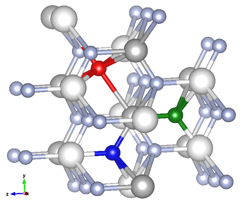
In the wurtzite structure, there are two high-symmetry interstitial sites, the tetrahedral one, located vertically between a cation and anion in the -direction in two successive A layers of the ABAB stacking, and an octahedral one, located in the big open hexagonal cross-section channels, when viewed from the -direction. In ZnGeN2, there are furthermore two types of tetrahedral interstitials depending on whether it occurs between a Zn and N or a Ge and N (Fig. 1). We found in our relaxation calculations that both Zn and Ge strongly prefer the large octahedral sites. When we start out an interstitial in the tetrahedral site it is unstable and moves toward the octahedral site. Our results for both these cases thus correspond to the octahedral site.
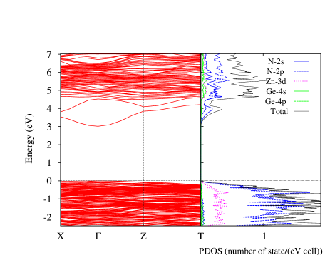
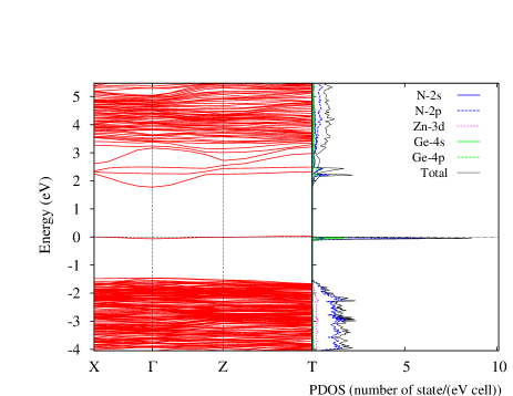
We start by discussing the one-electron energy levels or defect band structures of the supercells. The band structure and partial density of states (PDOS) for Zni are shown in Fig. 2 for the charge state.
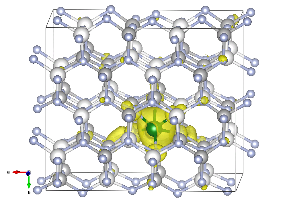
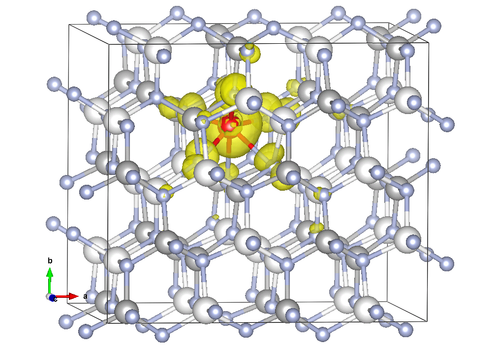
We can see that there are no defect levels in the band gap, but a peak in density of states slightly above the conduction band, and comparison to the perfect crystal band structure indicates a resonance in the conduction band. In the neutral and charge states, we find the Fermi level inside the conduction band, but for the state, it occurs at the valence band maximum (VBM). This indicates that Zni is a shallow double donor defect. Fig. 3 shows the wave function modulo squared for the second level above the conduction band minimum in the the state. This is a resonant level and is calculated as the contribution to the charge density from a small -space region around and over a narrow energy range. From its approximately spherical shape on the -site, we conclude it is mostly Zn- like. The results shown here for the bands are obtained in the LDA+U approach. Within the LDA, a similar result is obtained, (shown in Supplementary Information) except that the gap is correspondingly smaller. In other words the resonances in the conduction band shifted up along with the conduction band, which is as expected from their Zn--like orbital character.
| A | B | C | D | |
|---|---|---|---|---|
| -0.525 | 0 | 0 | -0.840 | |
| 0 | -0.35 | -0.626 | -0.066 | |
| -0.696 | -1.396 | -1.12 | 0 |
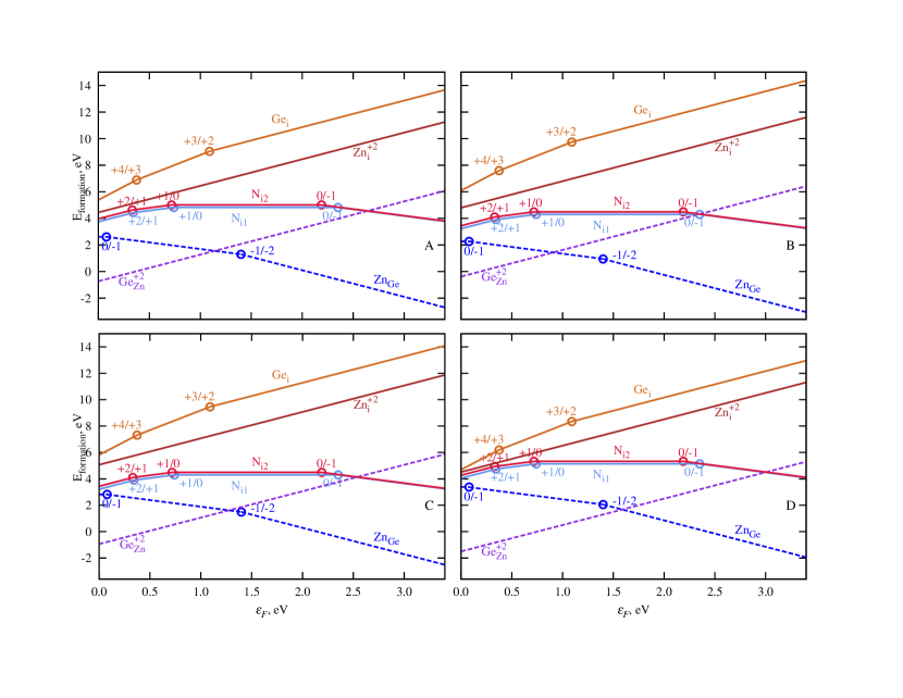
The corresponding energy of formation as function of Fermi level is show along with that of the other interstitials in Fig. 4. The various panels here correspond to different chemical potential conditions as defined in Fig. 1 of Ref. Skachkov et al., 2016a, summarized here in Table 1. The lines AB and CD mark the boundary with the region where Zn3N2 and Ge3N4 become the preferred phases, while the line BC corresponds to N-rich condition, marking equilibrium with N2 molecules. One can see that the Zni has the lowest energy of formation for case A, which is the most Zn-rich case, but in fact, does not vary very much because the range of allowed Zn chemical potentials is rather restricted. Similarly, Gei has the lowest energy of formation for the most Ge-rich condition D and Ni has the lowest energy of formation both B and C. For comparison, this figure also includes the energies of formation of the ZnGe and GeZn antisites, which are the lowest energy defects found in Ref. Skachkov et al., 2016a. For the Zni, only the charge state occurs in the gap.
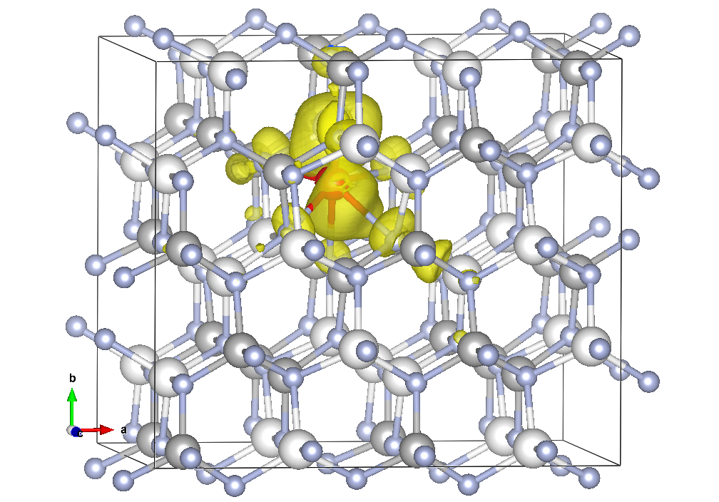
Next, we consider the Gei bands and PDOS in Fig. 5 within LDA+U. We show it again for the charge state. In contrast to the Zni, we now see a sharp defect level about 1.5 eV above the VBM. For the neutral charge state, again there would be electrons in the CB but now the and charge states also could occur by depleting the defect level in the gap. Fig.6 illustrates some of the relevant wave functions. These orbital shapes are almost the same in LDA or LDA+U. They are here shown for LDA. The HOMO of the charge state corresponds to the defect level in the gap and is clearly localized around the Ge interstitial. However, the HOMO+2 and HOMO+3 above the conduction band indicate there are also resonances in the conduction band. The deep level in the gap has mostly Ge- character as can be seen from its more or less spherical looking charge density contribution on the Ge site. In contrast, the resonances in the conduction band have Ge- character. Both defect states are seen to also have some admixture of neighboring N- states. Comparing to LDA, (see Supplementary Information) we find that the defect level in the gap moved up by the LDA+U correction from 0.53 eV to 1.40 eV. This shift of 0.9 eV should be compared with the gap shift of 1.2 eV. It shows that although this level lies deep below the CBM it is still strongly shifting along with the CBM, which is consistent with its Ge- character. This shift also affects the positions of the transition levels, shown in Fig. 4. For the latter, we note that an effective charge of was used for the charge state to best match the distance dependence of the electrostatic potential. The choice of affects the position of the transition state. We estimate that this may lead to an uncertainty of order a few 0.1 eV on these transition levels.
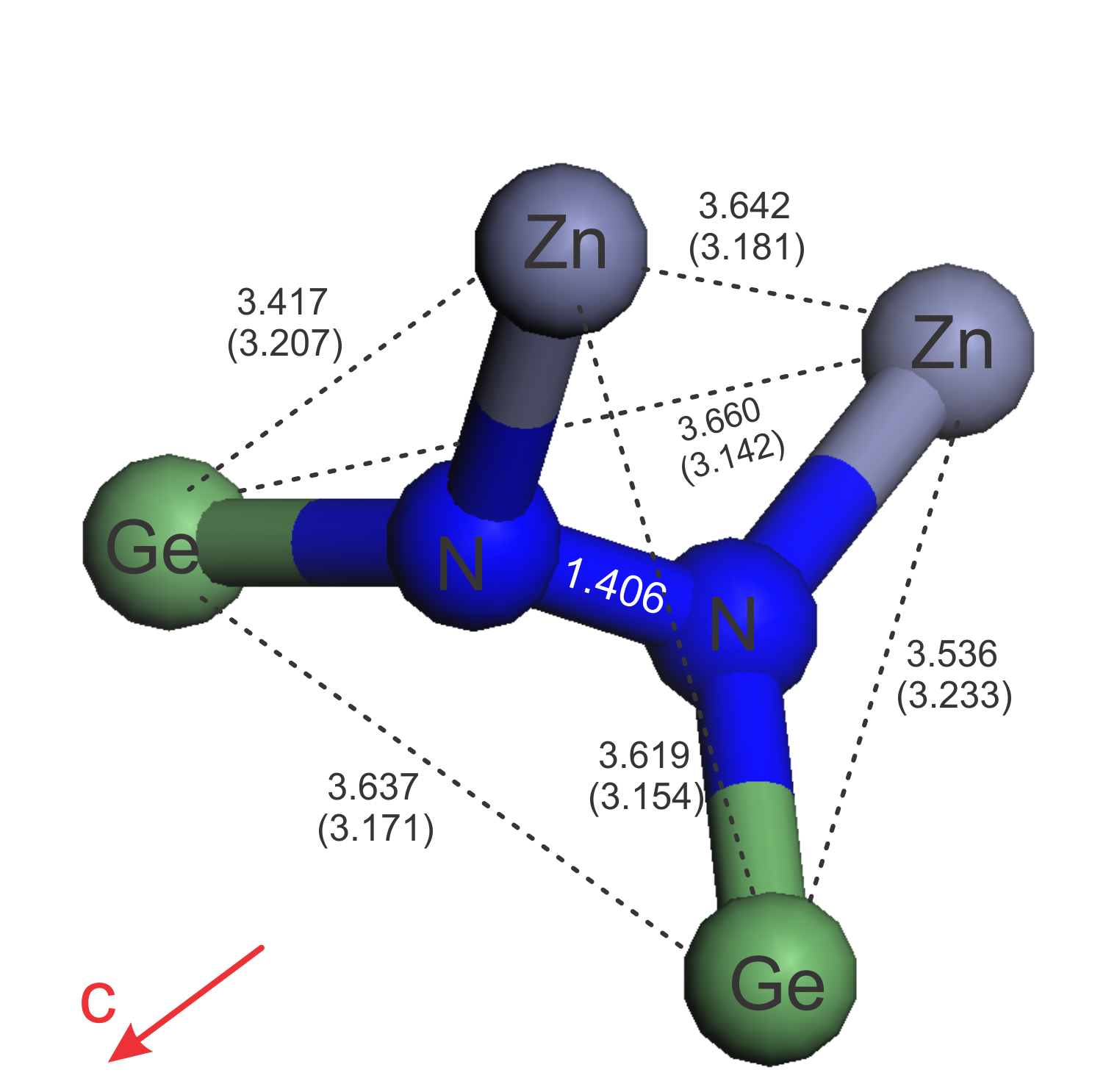
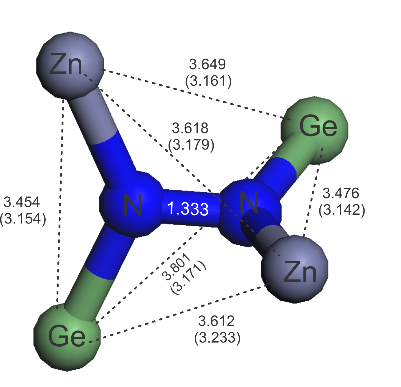
The interstitial Ni turns out to have a more interesting relaxation behavior than the Zni or Gei which show only small displacements of the neighboring atoms. In fact, the Ni forms a split-interstitial configuration where a N2 dumbbell replaces the -site. In other words, the N interstitial displaces one of the neighboring N lattice sites by forming a bond with it. This is shown in Fig. 7 which shows the bond-lengths for the two slightly different N interstitial configurations we found. The first one, corresponds to N2 replacing the NZn which sits above a Zn, atom in the -direction. The second one, corresponds to a N2 sitting above a Ge. The latter has a slightly shorter N2 bond length but both are larger than in a free N2 molecule, which has a bond length of 1.10 Å.
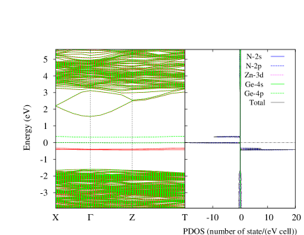
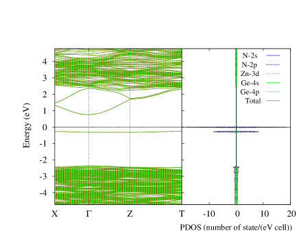
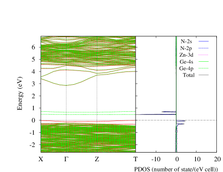
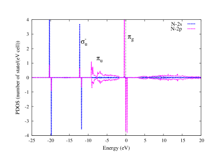
Fig. 8 shows the energy levels and PDOS for the Ni2 configuration as an example and obtained within LDA+U and including spin-polarization. (Results within LDA are given in Supplementary Information.) The results for the other one are similar. We can see two closely spaced defect levels in the gap for each spin. Fig. 9 shows the N2 projected PDOS on a wider energy scale, from which we can identify the molecular orbitals of the N2 molecule, as indicated by the labeling. It shows that the states in the gap correspond to the state, which in the N2 molecule would be the lowest unoccupied molecular orbital (LUMO). As expected, since this N2 molecule now plays the role of a N ion in the crystal, it accommodates three extra electrons, and thus the neutral charge state of the defect, in a nominal sense corresponds to the N state of the molecule. Of course, the charge will be spread out somewhat to neighboring atoms. We can also see this from Fig. 8. In fact, in the neutral charge state, the Fermi level coincides with the lower minority spin level, thus the levels are occupied with 3 electrons. In the LDA and non-spin-polarized calculation, the level passes through the upper defect level band. On the other hand, in the state all levels in the gap are filled and a state results. Finally, in the , we have two electron in the lower levels. They can in principle have a or state. We find the latter to have the lower energy, resulting in a high-spin state of the defect. When this state is further emptied, a state with is also found to give a transition level in the gap.
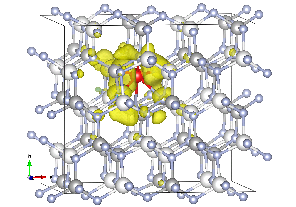
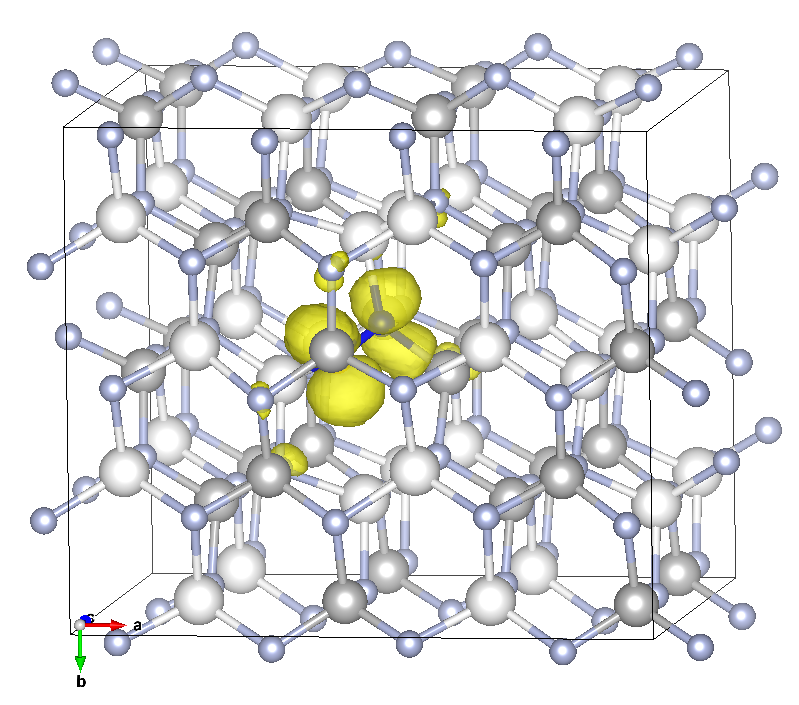
The energies of formation in Fig. 4 show the corresponding transition levels , and . The occurrence of both +1 and charge states, shows that this is an amphoteric trap level: it can both catch holes and electrons. The wave function plot in Fig. 10 for the neutral charge states corresponds to the upper level and confirms the N2 -like molecular state character of this level. The second level looks almost identical and is therefore not shown. The slight splitting of this level results from the interaction with the crystalline environment which lowers the symmetry compared to the free molecule and hence, splits the 2-fold orbital degeneracy of the -state. For the interstitial, the results are similar but the defect levels split slightly more. This difference corresponds to the slightly different bond distances of the N atoms to the neighboring Zn and Ge.
Comparing with the LDA approach we find that the Ni defect levels stay at approximately the same energy relative to the VBM (they move up by only 0.2 eV due to the terms) while the CBM moves up significantly. This is consistent with the deep and N- character of this defect. On the other hand, including the spin-polarization effects of these levels is important.
In Table 2 we give the energies of formation, corresponding to the chemical potential condition C. Compared with the energies of formation of the vacancies and antisites, which were studied in Ref. Skachkov et al., 2016a, we see that the interstitials have higher energy of formation than the antisites. They thus will play little role in the determination of the Fermi level of the native material, which is dominated by the low energy of formation antisite competition. While these defects, having high energy of formation are thus not expected to occur in large concentrations in equilibrium, they are nonetheless important because they could be formed under irradiation or ion bombardment. The transition levels are summarized in Table 3.
| Defect | =0) | |
| Zni | 2 | 4.51 |
| Gei | 2 | 6.16 |
| 3 | 5.07 | |
| 4 | 4.69 | |
| Ni1 | 0 | 5.14 |
| 1 | 4.40 | |
| 2 | 4.05 | |
| -1 | 7.49 | |
| Ni2 | 0 | 5.33 |
| 1 | 4.61 | |
| 2 | 4.28 | |
| -1 | 7.52 |
| Defect | Transition levels | ||
|---|---|---|---|
| +2/+1 | +1/0 | 0/-1 | |
| Ni1 | 0.34 | 0.74 | 2.35 |
| Ni2 | 0.33 | 0.72 | 2.19 |
| +4/+3 | +3/+2 | ||
| Gei | 0.38 | 1.09 | |
IV Conclusions
In this paper, we studied the native interstitial defects in ZnGeN2. We found that both Zni and Gei defects behave as double shallow donors and prefer the octahedral interstitial site because of their size. However, Gei also has a deep level close to the VBM and can thus occur in a and even charge state. The level in the gap is Ge- like. Both defects have resonances in the CB which in the Zni case corresponds to Zn- but in the Gei case corresponds to Ge-. The Ni forms two slightly different split interstitials depending on its location, with slightly different effective N2 bond lengths. It has a level in the gap corresponding to the like LUMO of the N2 molecule and this level behaves amphoteric as a trap level, in other words, it can be both in positive and negative charge states. In its single positive charge, it prefers a high-spin state. The interstitials are all found to have higher energies of formation than the antisites, studied earlier and will hence not affect the position of the Fermi level because of their expected low concentration in equilibrium. In particular, they are not expected to contribute significantly to the background unintentional n-type doping found in most ZnGeN2 crystals.
Acknowledgements.
This work was supported by the U.S. National Science Foundation under Grant No. DMREF-1533957. The calculations were performed at the Ohio Super Computer Center under Project No. PDS0145.References
- Lambrecht and Punya (2013) W. R. L. Lambrecht and A. Punya, in III-Nitride Semiconductors and their Modern Devices, edited by B. Gil (Oxford University Press, 2013) Chap. 15, pp. 519–585.
- Punya et al. (2011a) A. Punya, W. R. L. Lambrecht, and M. van Schilfgaarde, Phys. Rev. B 84, 165204 (2011a).
- Quayle et al. (2015) P. C. Quayle, E. W. Blanton, A. Punya, G. T. Junno, K. He, L. Han, H. Zhao, J. Shan, W. R. L. Lambrecht, and K. Kash, Phys. Rev. B 91, 205207 (2015).
- Paudel and Lambrecht (2007) T. R. Paudel and W. R. L. Lambrecht, Phys. Rev. B 76, 115205 (2007).
- Peshek et al. (2008) T. J. Peshek, T. R. Paudel, K. Kash, and W. R. L. Lambrecht, Phys. Rev. B 77, 235213 (2008).
- Paudel and Lambrecht (2008) T. R. Paudel and W. R. L. Lambrecht, Phys. Rev. B 78, 115204 (2008).
- Paudel and Lambrecht (2009) T. R. Paudel and W. R. L. Lambrecht, Phys. Rev. B 79, 245205 (2009).
- Punya et al. (2011b) A. Punya, T. R. Paudel, and W. R. L. Lambrecht, physica status solidi (c) 8, 2492 (2011b).
- Jaroenjittichai and Lambrecht (2016) A. P. Jaroenjittichai and W. R. L. Lambrecht, Phys. Rev. B 94, 125201 (2016).
- Lyu and Lambrecht (2017) S. Lyu and W. R. L. Lambrecht, Phys. Rev. Materials 1, 024606 (2017).
- Du et al. (2008) K. Du, C. Bekele, C. C. Hayman, J. C. Angus, P. Pirouz, and K. Kash, J. Cryst. Growth 310, 1057 (2008).
- Zhu et al. (1999) L. Zhu, P. Maruska, P. Norris, P. Yip, and L. Bouthillette, MRS Internet J. Nitride Semicond. Res. 4S1, G3.8 (1999).
- Feldberg et al. (2012) N. Feldberg, B. Keen, J. D. Aldous, D. Scanlon, P. A. Stampe, R. Kennedy, R. Reeves, T. D. Veal, and S. Durbin, in Photovoltaic Specialists Conference (PVSC), 2012 38th IEEE (2012) pp. 002524–002527.
- Lahourcade et al. (2013) L. Lahourcade, N. C. Coronel, K. T. Delaney, S. K. Shukla, N. A. Spaldin, and H. A. Atwater, Advanced Materials 25(18), 2562 (2013).
- Quayle et al. (2013) P. C. Quayle, K. He, J. Shan, and K. Kash, MRS Communications 3, 135 (2013).
- Fioretti et al. (2015) A. N. Fioretti, A. Zakutayev, H. Moutinho, C. Melamed, J. D. Perkins, A. G. Norman, M. Al-Jassim, E. S. Toberer, and A. C. Tamboli, J. Mater. Chem. C 3, 11017 (2015).
- Qin et al. (2016) R. Qin, H. Cao, L. Liang, Y. Xie, F. Zhuge, H. Zhang, J. Gao, K. Javaid, C. Liu, and W. Sun, Applied Physics Letters 108, 142104 (2016), http://dx.doi.org/10.1063/1.4945728 .
- Deng et al. (2015) F. Deng, H. Cao, L. Liang, J. Li, J. Gao, H. Zhang, R. Qin, and C. Liu, Opt. Lett. 40, 1282 (2015).
- Senabulya et al. (2016) N. Senabulya, N. Feldberg, R. A. Makin, Y. Yang, G. Shi, C. M. Jones, E. Kioupakis, J. Mathis, R. Clarke, and S. M. Durbin, AIP Advances 6, 075019 (2016), http://dx.doi.org/10.1063/1.4960109 .
- Punya and Lambrecht (2013) A. Punya and W. R. L. Lambrecht, Phys. Rev. B 88, 075302 (2013).
- Han et al. (2016) L. Han, K. Kash, and H. Zhao, Journal of Applied Physics 120, 103102 (2016), http://aip.scitation.org/doi/pdf/10.1063/1.4962280 .
- Chen et al. (2014) S. Chen, P. Narang, H. A. Atwater, and L.-W. Wang, Advanced Materials 26, 311 (2014).
- Wang et al. (2017) T. Wang, C. Ni, and A. Janotti, Phys. Rev. B 95, 205205 (2017).
- Skachkov et al. (2016a) D. Skachkov, A. Punya Jaroenjittichai, L.-y. Huang, and W. R. L. Lambrecht, Phys. Rev. B 93, 155202 (2016a).
- Skachkov et al. (2016b) D. Skachkov, P. C. Quayle, K. Kash, and W. R. L. Lambrecht, Phys. Rev. B 94, 205201 (2016b).
- Hohenberg and Kohn (1964) P. Hohenberg and W. Kohn, Phys. Rev. 136, B864 (1964).
- Kohn and Sham (1965) W. Kohn and L. J. Sham, Phys. Rev. 140, A1133 (1965).
- von Barth and Hedin (1972) U. von Barth and L. Hedin, Journal of Physics C: Solid State Physics 5, 1629 (1972).
- Methfessel et al. (2000) M. Methfessel, M. van Schilfgaarde, and R. A. Casali, in Electronic Structure and Physical Properties of Solids. The Use of the LMTO Method, Lecture Notes in Physics, Vol. 535, edited by H. Dreyssé (Berlin Springer Verlag, 2000) p. 114.
- Kotani and van Schilfgaarde (2010) T. Kotani and M. van Schilfgaarde, Phys. Rev. B 81, 125117 (2010).
- Freysoldt et al. (2009) C. Freysoldt, J. Neugebauer, and C. G. Van de Walle, Phys. Rev. Lett. 102, 016402 (2009).
- Freysoldt et al. (2014) C. Freysoldt, B. Grabowski, T. Hickel, J. Neugebauer, G. Kresse, A. Janotti, and C. G. Van de Walle, Rev. Mod. Phys. 86, 253 (2014).
- Komsa and Pasquarello (2013) H.-P. Komsa and A. Pasquarello, Phys. Rev. Lett. 110, 095505 (2013).
- Kumagai and Oba (2014) Y. Kumagai and F. Oba, Phys. Rev. B 89, 195205 (2014).
- Anisimov et al. (1991) V. I. Anisimov, J. Zaanen, and O. K. Andersen, Phys. Rev. B 44, 943 (1991).
- Liechtenstein et al. (1995) A. I. Liechtenstein, V. I. Anisimov, and J. Zaanen, Phys. Rev. B 52, R5467 (1995).