Aharonov-Bohm oscillations and magnetic focusing in ballistic graphene rings
Abstract
We present low-temperature magnetotransport measurements on graphene rings encapsulated in hexagonal boron nitride. We investigate phase-coherent transport and show Aharonov-Bohm (AB) oscillations in quasi-ballistic graphene rings with hard confinement. In particular, we report on the observation of , and conductance oscillations. Moreover we show signatures of magnetic focusing effects at small magnetic fields confirming ballistic transport. We perform tight binding calculations which allow to reproduce all significant features of our experimental findings and enable a deeper understanding of the underlying physics. Finally, we report on the observation of the AB conductance oscillations in the quantum Hall regime at reasonable high magnetic fields, where we find regions with enhanced AB oscillation visibility with values up to %. These oscillations are well explained by taking disorder into account allowing for a coexistence of hard and soft-wall confinement.
pacs:
???I Introduction
Quantum interference and ballistic transport are corner stones in mesoscopic physics imr02 giving rise to many interesting effects, such as weak localization corrections, universal conductance fluctuations,lee85 quantized conductance,wee88 persistent currents,ble09 Aharonov-Bohm oscillations web85 and many others. These effects are known to depend strongly on system size and characteristic length scales of electron transport, such as the elastic mean free path and the phase-coherence length. As these length scales are crucially affected by impurity and defect scattering as well as by electron-phonon and electron-electron interactions, high-purity materials and low temperatures are vital for controlling and utilizing quantum interference phenomena in mesoscopic systems. For experimentally adressing these phenomena two-dimensional (2D) electron systems based on III-V heterostructures have proven as a very favorable platform.
Thanks to the recent advances in process technologies for assembling 2D materials,gei13 we nowadays have bulk graphene samples with elastic mean free paths exceeding values of 25 .ban16 These advances not only start closing the gap between graphene and the most favorable GaAs-based 2D electron-systems but they also open the door to Dirac fermion-based mesoscopic devices with a hard-wall confinement and to a unique platform for electron-optics.agr13 ; bog17 Recently a number of interesting devices and phenomena based on ballistic transport in graphene have been demonstrated, ranging from Fabry-Perot and commensurability oscillations,you09 ; han17 to magnetic focusing tay13 and the Veselago lens lee15 to Klein tunneling transistors wil14 and even ballistic graphene Josephson junctions. bor16 All these devices rely on high-mobility graphene with large lateral dimensions such that edges are not limiting transport.
In this work we show that ballistic transport in state-of-the-art graphene can also be maintained when carving out mesoscopic rings, allowing to study electron interference in mesoscopic devices with a truely hard-wall confinement and a widely tunable Fermi wave length. In particular we present low-temperature magneto-transport measurements on graphene rings exhibiting ballistic transport, Aharonov-Bohm conductance oscillations and magnetic focusing. Aharonov-Bohm (AB) interference aha59 experiments on ring structures have been proven to be useful for observing and controlling interference patterns as they provide a straightforward way for shifting the phase by a small out-of-plane magnetic field. The AB effect has been studied in detail in rings based on metallic films,web85 semiconductor heterostructures tim87 and more recently also on graphene.rus08 ; hue09 ; hue10 ; smi12 ; cab14 Here it is important to note that in all previous studies on graphene rings, the samples have been in the diffusive regime, which in contrast to ballistic transport (i) leads to a strong suppression of AB oscillations at very low carrier densities,rus08 (ii) does not allow to access magnetic focusing, and (iii) prohibits the probing of the coexistence of hard- and soft-wall confinement.
As graphene only consist of surface atoms, the sample quality is highly influenced by disorder arising from substrate interaction and edge roughness.sta09 ; gal10 By fully encapsulating graphene in hexagonal boron nitride (hBN) the sample quality is improved substantially.dean10 ; mayo11 ; pono11 ; wang13 Importantly, this improvement also holds for hBN-graphene-hBN structures with lateral dimensions down to around nm.ter16 For smaller structures disorder due to the rough edges of graphene leading to localized states strongly limits high mobility transport.eng13 ; bis15 ; ter16 Our work is based on this recent insights and we report (i) on the fabrication of graphene rings fully encapsulated in hBN, (ii) phase-coherent transport with focus on AB oscillations for small magnetic fields and (iii) on the observation of electron guiding and magnetic focusing for intermediate magnetic fields indicating quasi-ballistic transport. Moreover, we perform tight binding calculations of graphene rings with similar geometries and compare the simulation results with the measurements, being able to assign specific skipping orbits to signatures in the measured conductance traces. Finally, we discuss highly visible AB oscillations at the onsets of well established quantum Hall plateaus in experiment and theory.
II Methods
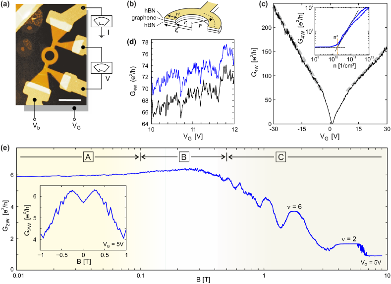
We present measurements on two samples with different geometry. Unless stated otherwise data from sample #1 are shown. The samples have been fabricated by stacking mechanically exfoliated graphene and hBN with the dry transfer technique based on van-der-Waals adhesion introduced by Wang et al. wang13 on highly p-doped Si substrates with a 285 nm thick SiO2 top layer. The hBN-graphene-hBN sandwiches have been structured by reactive ion etching (SF6/Ar plasma) using an AZ nlof 2020 mask patterned by electron beam lithography (EBL). Electrical contacts to the etched devices have been made by a second EBL step, metal evaporation (5 nm Cr/95 nm Au) and standard lift-off process. A scanning force microscopy (SFM) image of the final device #1 is shown in Fig. 1(a). From the SFM image we extract an inner and an outer ring radius of nm and nm, respectively (see also Fig. 1(b)). These numbers results in a mean radius of nm and a width of the ring arms of nm. The second sample has slightly different dimensions exhibiting a mean radius of nm and a width of the ring arms of nm. All measurements are performed in a dilution refrigerator with base temperature of around mK and perpendicular magnetic field up to T using standard low-frequency lock-in techniques for simultaneous two (2W) and four-terminal (4W) measurements. The two-terminal current is measured with a home build I/V converter and a low noise amplifier in combination with a standard lock-in amplifier, whereas the four-terminal voltage drop is measured directly by the lock-in as illustrated in Fig. 1(a). For the data analysis of the magnetic field dependent measurement we mainly concentrate on the two-terminal measurements, as the data quality is better thanks to pre-amplification.
The quantum transport simulation have been performed using a tight-binding approximation on a hexagonal lattice with the Kwant package.kwant We have simulated a scaled version of the graphene lattice with a lattice constant that is a factor 10 larger than the experimental situation and our simulation involves in total lattice sites. All results are presented in original units for easier comparison to the experimental findings. For more details on the simulation methodology, see Appendix 1.
III Results and Discussion
Figure 1(c) shows the four-terminal back-gate characteristics for zero magnetic field at base temperature. At high gate voltage we observe a linear dependence of the four-terminal conductance as function of with a slope of , (see dashed lines). We conservatively estimate the square conductance from the sample geometry FNgeometry . As the charge carrier density is directly linked to by , we find the field effect mobility by . Here, cm-2V-1 is the gate lever arm, which has been extracted from quantum Hall measurements (see below), is the elementary charge and the charge neutrality point (CNP) is around V. We obtain field effect mobilities of cm2V-1s-1 for hole and cm2V-1s-1 for electron transport. These mobility values correspond to a mean free path in the range of nmm (for V) FNmfp highlighting that the transport can be considered as quasi-ballistic (, where is the sample length exceeding ) and that the approximate diffusive description only holds due to diffusive scattering at the rough edges. With the Einstein relation we estimate the diffusion constant , where is the density of states of graphene. By following Ref. rus08, we express as function of and obtain , where m/s is the Fermi velocity and the Planck constant. For electron transport we thus extract a diffusion constant of m2/s (for V). These values are close to the value of the diffusion constant only taking into account diffusive scattering at the edges of the narrow leads and the ring arms ( m2/s). The high sample quality is moreover reflected in the low residual charge carrier density found to be in the order of cm-2, extracted as shown in the inset of Fig. 1(c).cou14 By having a closer look at the four-terminal back-gate characteristics we observe well reproducible universal conductance fluctuations (UCFs) with an amplitude of up to (see Fig. 1(d), a close-up of Fig. 1(c)). The UCFs are a strong evidence for phase-coherent transport.
In Fig. 1(e) the two-terminal conductance is plotted as function of magnetic field at V in the near vicinity of the CNP. For small magnetic fields we observe a nearly linear increase of as function of (see inset in Fig. 1(e)) with reaching a maximum at T. At higher -fields we observe signatures originating from the quantum Hall effect. As the two-terminal conductance contains contributions from the longitudinal and the Hall conductance we observe dips before entering quantum Hall plateaus, which are typical for two-terminal devices, where the sample length is larger than the width (sample #1 nm to several m).aba08 Quantum Hall plateaus are well visible for filling factors (see labels in Fig. 1(d)). The difference in conductance with respect to the theoretically expected plateaus at and is due to additional resistances from the setup and the contact resistance of the graphene-metal interface included in the two-terminal measurement. With the known setup resistance k, we estimate an overall contact resistance of for each contact.
To systematically discuss the magnetic field dependent conductance measurements we divide the -field range into three regimes based on the ratios of the width of the ring arms (as well as the mean ring radius ) and the cyclotron radius (here the reduced Planck constant). First (Sec. III.A) we focus on small -fields such that . In this regime (see label A in Fig. 1(e)) we mainly concentrate on AB oscillations and their dependence on charge carrier density. Second (Sec. III.B) we discuss magnetic focusing and localization effects in the regime, where the cyclotron radius is on the order of and (i.e. ), see label B in Fig. 1(e). Third (Sec. III.C) we focus on quantum interference phenomena in the quantum Hall regime (label C), where is significantly smaller than and . In particular, we require for entering the regime of quantum Hall edge transport.
III.1 Aharonov-Bohm oscillations at low -fields
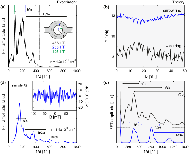
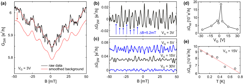
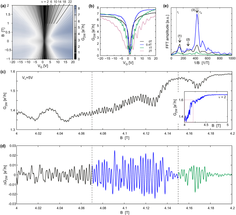
Figure 2(a) shows the two-terminal conductance as function of magnetic field in the small magnetic field range mT at V. In this regime we observe the presence of AB oscillations as well as UCFs and an overall increase of the conductance with absolute value of magnetic field. As the change of conductance due to AB interference is on the order of a few percent and overlapping with UCFs, additional data post-processing is needed to extract the periodicity and the amplitude of the AB oscillations . We apply a moving average over a window of mT, which is sufficiently larger than the expected periodicity mT for the mode FNabo and subtract the averaged data from the raw signal (see red dashed line in Fig. 2(a)). Fig. 2(b) displays the processed data of the two-terminal conductance versus magnetic field . In this plot horizontal lines with a spacing of mT indicate the expected periodicity of the AB oscillations for an ideal ring device with a radius of nm, which corresponds to the mean radius of our fabricated graphene ring. In general, the conductance oscillations are found to be mainly equidistant, but also additional modulations and local derivations are observed. Figure 2(c) depicts similar data, but for different gate voltages (see labels). Interestingly, for higher gate voltages the AB amplitude decreases, while the periodicity is preserved. This observation is summarized in Fig. 2(d), where is plotted as function of . Here is defined as the root mean square amplitude of . Strikingly, the maximum visibility FNvisib is found close to the charge neutrality point at V and is around with respect to the overall conductance . Although the maximum two-terminal visibility is similar to earlier experiments on diffusive graphene rings,rus08 ; cab14 the carrier density dependency is inverted. For example, in contrast to Ref. rus08, we observe a decreasing amplitude for increasing gate voltage . We explain this behavior by an increasing asymmetric transmission through the two ring arms coming along with an increasing mean free path as function of carrier density. Entering the quasi-ballistic transport regime, the transmission through each of the two arms depends on the specific microscopic sample shape and disorder potentials. Therefore, the transmission is not symmetric, leading to a reduced visibility of AB oscillation vas07 . Also with increasing charge carrier density the Fermi wavelength is decreasing allowing a higher number of wave modes inside the ring, which may also decrease as it is observed in semiconductor heterostructures.for88 In Fig. 2(e), is plotted as function of temperature at V. The decrease of the amplitude with an increase of follows an overall dependence. Due to thermal averaging of the oscillations and changes in the phase-coherence length , the AB amplitude decays as , where is the Thouless energy and the Boltzmann constant.rus08 In a diffusive system, is given by with characteristic lenght scale . Using the diffusion constant determined above m2/s (for V)and , we estimate eV, which corresponds to a critical temperature of mK. Without thermal averaging the phase-coherence length is primarily limited by electron-electron scattering following a temperature dependence given by as also reported for ballistic one-channel rings in GaAs heterostructures.han01 Thus, a decay of the AB amplitude is expected below which is in reasonable agreement with our observation in Fig. 2(e). Due to a limited accessible temperature range we can not extract from the data and determine the energy scale, when thermal averaging contributes to decoherence of AB oscillations.
For further analysing the AB oscillations we preform fast Fourier transformation (FFT) of the processed data, as shown exemplarily for V in Fig. 3(a). The Fourier spectrum shows a broad band of frequencies that constitute the signal. Peaks for frequencies below the expected AB oscillations, which we attribute to artifacts from the data averaging of a mT moving window (corresponding to 1/T) are neglected in the further discussion. The interval of the mode frequencies is given by the sample geometry ranging from to 1/T as indicated in Fig. 3(a). The main contribution is around the frequency related with the mean radius of the ring, although features at lower and higher frequencies are present. The broad spread is due to the aspect ratio of mean radius and the width of the ring, . Notably, this circumstance makes any attempt to distinguish contributions from the and mode difficult as the differences in enclosed area for different paths overlap (see also horizontal arrows in Fig. 3(a)). This experimental observation is also well reproduced by tight binding calculations as describe above (see Fig. 3(b)). In the simulations, the AB oscillations exhibit a higher amplitude than in the experiment, which we attribute to the perfectly symmetric transmission through both ring arms and the lack of any other experimental limitations, such as bulk disorder and contact resistance mentioned above. These effects are not included in the calculations since they are not relevant to the investigated physics. The overall behavior of the conduction fluctuations in the wider ring is comparable to the experimental data and the FFT analysis gives similar results (compare black traces in Figs. 3(a) and 3(c)). Again, a broad range of frequency components is observed in the given ranges of AB mode making a clear assignment of FFT peaks to mode number more than difficult. The narrower ring with a larger aspect ratio ( nm, nm) exhibits a lower amplitude in the calculations, but more distinguishable peaks in the FFT spectrum (compare traces in Fig. 3(c)). Now peaks only appear close to the center of the corresponding mode ranges and are unambiguously identified as the fundamental mode and its multiples. Since decoherence, i.e. dephasing is not implemented in the simulation, many higher harmonics are visible. To confirm these results we measured AB oscillations in sample #2 which has a larger aspect ratio . Figure 3(d) displays the FFT spectrum of sample #2 at similar as Fig. 3(a). The ranges of and conduction oscillations only overlap slightly and peaks of the fundamental mode and the first and second harmonic are observed. In particular, the fact of observing contributions conductance oscillations (see label in Fig. 3(d)) allows for the conclusion that the phase-coherence length exceeds the value of . Hence the difficulties of AB mode identification for sample #1 arise from the ring geometry and does not primarily reflect on the sample quality and the phase-coherence length.
III.2 Ballistic electron guiding and magnetic focusing
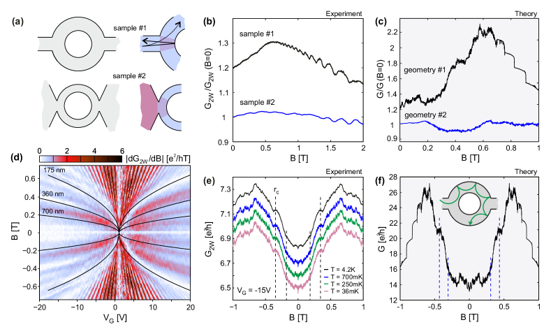
For magnetic fields of up to T we observe an increase of the magnetoconductance before a decrease evolves while entering the quantum Hall regime. In Figs. 4(a) and 4(b) this effect is shown for the two samples at similar charge carrier density cm-2 but different geometries, which differ in the type of connecting the ring structure to the source and drain leads and the width of the ring arms. Sample #1 consists of a kind of a T-junction comparable to geometries used in previous experiments for graphene rings on silicon dioxide rus08 ; hue09 ; hue10 while sample #2 is based on a V-shaped connection similar to experiments on III-V heterostructures grb07 . The changes in with are more pronounced in sample #1 with the T-junction, while they are hardly visible in sample #2 (see Fig. 4(b)). The increase in magnetoconductance for sample #1 is caused by an increase of the average mode transmission as function of -field at the T-junction. From a semiclassical point of view this observation is connected to the fact that straight trajectories ( T) are more likely reflected at the T-junction than curved once ( T), as illustrated in Fig. 4(a) (see solid and dashed trajectories in the upper right panel). This effect, however, is strongly reduced in sample #2 because there are many open modes available in the lead region very close to the ring, making transport not very sensitive to the average mode transmission as the overall conductance is limited only by the number of modes in the ring arms (compare different colors in the right panels of Fig. 4(a)). In other words, there are in any case enough trajectory angles available for entering the ring via the V-shaped connection. These observations support the assumption of quasi-ballistic transport (), because magnetic focusing requires a mean free path larger than the width of the ring. In simulations with similar device geometries — geometry #1 (T-geometry with nm, ) and geometry #2 (V-geometry with nm, nm) and comparable charge carrier density cm-2 — we find good qualitative agreement with our experimental findings (see Fig. 4(c)). The simulations show an increase in magnetoconductance before entering the quantum Hall regime for the T-junction geometry (#1) and an almost constant curve for the V-shape geometry (#2). Steps indicating the beginning of the quantum Hall effect occur for geometry #1 at T, whereby for the narrower geometry #2 they start at T since a smaller cyclotron radius is required (not shown). Intrinsic restrictions of the simulations, such as zero temperature, infinite phase-coherence length and negligence of contact resistance, lead to additional features. At zero temperature UCFs are enhanced leading to more wobbly traces. Also Shubnikov-de Haas oscillations are not visible due to the absence of thermal broadening of the Landau levels. In general the simulation results coincide with the experimental observation and the effect is attributed to the interplay of focusing of charge carriers by magnetic field and the type of connection between ring and leads, which is refereed to as a size effect. In these measurements we find also plateau-like features in the rising magnetoconductance below T indicating another size effect related with magnetic field.
Figure 4(d) depicts the derivative of conductance with respect to magnetic field as function of and in a color plot. Here, several features are identified, which show a dependence as the cyclotron radius . As a guide to the eye constant cyclotron radii are drawn in Fig. 4(d) using the gate lever arm determined from Landau fan measurements (see below). At nm the cyclotron radius matches the requirement for the formation of edge states () and we observe the transition to the quantum Hall effect exactly at this limit. In the regime of larger cyclotron radii () we interestingly observe constant conductance plateaus () in the -field dependent increasing magnetoconductance, which coincide with and nm, respectively. For further investigations versus is measured at fixed gate voltage V ( cm-2) for different temperatures mK, mK, mK and K (see Fig. 4(e)). For all temperatures the traces are very similar and only differ in the amplitude of the UCFs and AB oscillations, which almost vanish for K. At mT a conductance plateau is observed, which corresponds to a cyclotron radius of nm. A second conductance plateau is located at mT (corresponding to nm), but only visible at K due to the superposed AB oscillations at lower temperatures. Since the plateaus are observable even in the absence of UCFs and AB oscillations, we conclude that they do not require phase-coherent transport.
The high carrier mobility and the dependency on cyclotron radius indicate that the conductance plateaus are linked to magnetic focusing of charge carriers inside the ring structure.tay13 In this case the trajectories of the carriers are deflected by the magnetic field and for some cyclotron radii it becomes more unlikely to exit the ring, which yield in a suppressed increase of magnetoconductance. A schematic illustration of an example of such a trajectory is shown in the inset of Fig. 4(f). For confirming our observation, we carried out tight binding calculation in the intermediate magnetic field regime. Figure 4(f) shows corresponding simulations for the data shown in Fig. 4(e). Here the conductance plateaus are reproduced quantitatively (compare vertical dashed lines in Figs. 4(e) and 4(f)) by assuming finite edge roughness of the graphene ring. The edge roughness introduced by the lithographic pattering of the graphene sheet affects the visibility of the focusing effect and a further analysis of its impact on the simulation results can be found in Appendix 3. The smooth steps in the falling edge after the maximum conductance are due to the emerging quantum Hall effect and are not related to magnetic focusing or size quantization effects. Similar observations of magnetic focusing have been made in an AB ring in a GaAs quantum well, where also a T-junction has been used and these effects have been attributed to quasi-ballistic transport with boundary scattering.mur08 This type of boundary scattering is quite surprising in consideration of the lithographically etched sample outline and the requirement for specular scattering, that the roughness of the boundaries must be smaller than the Fermi wavelength .bee91 Thus the spatial extension of the disorder potential from the device edge must be smaller than , since the focusing feature is still present at gate voltage , which correspond to and , respectively. In summary, our experimental findings and simulation results point in exactly this direction and strongly support the observation of magnetic focusing in a quasi-ballistic ring system.
III.3 High-visibility AB oscillations near QH plateaus
Next we focus on the high -field regime (). Figure 5(a) shows a 2D color plot of as function of and . We observe a graphene-typical Landau fan for two-terminal measurements with integer Hall plateaus and filling factors up to for T. The observation of clear and pronounced features in the Landau fan at such low magnetic fields presupposes a very homogenous doping level, which is also reflected in the low extracted (see above). Following Ref. ki12, we extract the capacitive coupling or so-called lever arm of the back gate from the slope of the Landau levels, which results in cm-2V-1 and is in good agreement assuming a parallel plate capacitor model.
In Fig. 5(b) we show several traces of as function of for various -fields. Quantum Hall signatures are evolving in the vicinity of the CNP below T and are fully developed at T. The dips in magnetoconductance between the conductance plateaus are due to the sample geometry as described above. For T the conductance plateaus are more pronounced, but also an asymmetry between the hole and electron transport regime becomes apparent, whereas the origin of this remains unclear.
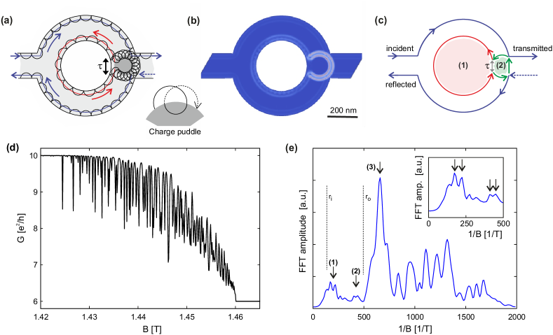
In the -field range of fully developed quantum Hall plateaus, we find a substantial increase in the visibility of AB oscillations for specific settings of and (see Fig. 5(c)). This effect takes place at the flanks, i.e. onsets of quantum Hall plateaus and is observed only for a few different -field and gate voltage values. The AB amplitude changes by a factor of for small changes in -field on the order of a few tens of milliteslas indicating that they are sensitive to sample inhomoginities. Figure 5(d) depicts of the data shown Fig. 5(c). In the best region the AB amplitude reaches a visibility of more than , which is a significant increase compared to the low field regime (). This becomes even more apparent in the FFT spectra of the different ranges. Figure 5(e) shows the corresponding FFT spectra and we observe an increase of the FFT amplitude by a factor of three or more. The distinct peaks in the FFT spectra (see e.g. blue trace in Fig. 5(e)) moreover show that there are very distinct enclosed areas contributing to the AB oscillations. This is overall in line with edge channel dominated transport. Interestingly we find (i) that there is one conductance oscillation frequency (labeled with (1) in Fig. 5(e)) which can be associated with the area enclosed by an edge mode along the inner radius (see vertical dashed line in Fig. 5(e) and red circle in the schematic illustration in Fig. 6(a)) and (ii) that the most pronounced peak in the FFT can be hardly associated and explained with an edge channel traveling along the outer radius (see vertical dashed line). This is on one hand because peak (3) includes area contributions larger than and on the other hand it is impossible to close such an area by pure edge channel transport. The latter point is also crucial when considering mechanisms which allow to access (i.e. to connect to) an edge channel propagating along the inner edge of the ring structure (see red circle in Fig. 6(a)).
Consistent with the observation that the conductance oscillations are only present in the crossover regime from one to another filling factor we assume that the disorder potential in the ring entrance or exit region is playing an important role. A present disorder landscape indeed may allow for both (i) accessing the inner edge channel and (ii) connecting the upper and the lower ring arm (see Fig. 6(a)). Such a disorder potential is known to arise from substrate interaction, contaminations or rough edges.mar07 It is very likely that in our case there is just one dominating ”‘charge puddle”’ connecting the two edge states, as scanning tunneling microscopy studies have shown that in graphene on hBN such disorder induced puddles have typical diameters of around nm,xue11 which is on the order of .
For a more detailed discussion we performed calculations of magnetotransport through an ideal ring structure (no edge roughness, ) with similar dimensions ( nm, nm) and include one charge puddle with a diameter of nm located at the exit region of the ring (see Fig. 6(a)). In Fig. 6(b) the calculated local density of states in the quantum Hall regime is plotted for a charge carrier density of cm-2 including a charge puddle with an offset in charge carrier density of cm-2 sitting right in the exit region of the ring (see Figs. 6(a) and 6(b)). Using this charge carrier density for Kwant simulations of magnetotransport the effect of enhanced visibility of AB oscillations is reproduced in qualitative manner (see Fig. 6(d)), where AB oscillations become most visible between two conductance plateaus (in this example at the step from filling factor 10 to 6). Again, many oscillations are observed with a maximum amplitude in the middle between two quantum Hall plateaus. In Fig. 6(e) we show the corresponding Fourier spectrum of the background subtracted conductance and the spectrum exhibits a surprisingly similar peak structure as seen in the experiment (see labels (1), (2) and (3) in Figs. 5(e) and 6(e)). In Fig 6(e) we can again identify a frequency contribution corresponding to the area enclosed by the quantum Hall channel around the inner radius of the ring (see left vertical dashed line and label (1) in Fig. 6(e)) while the most pronounced peak is at higher frequency value, exceeding an enclosed area of (see right vertical dashed line). By making use of our model system we can explain the enclosed area leading to the main peak (3) as being the sum of the two areas (1) and (2). The first area (1) corresponds to the edge channel going around the inner ring. The second area (2) originates from the motion around the charge puddle (see schematic illustrations in Figs. 6(a) and 6(c)). Notably, the second contribution (see also labels (2) in Figs. 6(e) and 5(e)) gives rise to a higher frequency compared to the one due to the inner ring radius even though its geometrical area is smaller. This is due to the different confinement of the edge channel (see schematic illustrations in Fig. 6(a)). While the confinement due to the graphene edges is a hard confinement with the edge modes corresponding to classical skipping orbits, the confinement along the charge puddle is a soft confinement corresponding to a cycloid motion (full cyclotron orbits that are drifting as shown by the inset in Fig. 6(a)). In a semiclassical description, the cycloid motion encloses a much larger area than the area enclosed by the guiding center. In particular, in a simplified model of the electron drift, the charge puddle has a different but constant filling factor and half of each cyclotron orbit is on either side of the interface. A single cyclotron orbit encloses an area of . The drift is given by twice the difference of the cyclotron radius, i.e., where is the charge carrier the density and the difference in carrier densities of the bulk and the charge puddle. Thus, the electron motion encloses the effective area due to the cyclotron motion, where is the length of the quantum Hall edge channel, additional to the geometric area of the charge puddle enclosed by the guiding center. In the present case, even dominates over the geometric size of the charge puddle resulting in the surprising effect that the peak (2) is due to the (small) charge puddle whereas (1) is due to the (large) inner radius of the ring. We have numerically checked that the dominant Aharonov Bohm frequency of the charge puddle alone without inner ring is 1/T that corresponds to the peak (2). Including the effect of the inner ring, the dominant contribution (3) is due to electrons encircling both the charge puddle as well as the inner ring. However, due to a finite tunneling coupling (see illustrations in Figs. 6(a) and 6(c)) along the charge puddle and the boundary of the inner ring, also the fundamental frequencies (1) and (2) contribute slightly to the Fourier transform. Interestingly, by having a closer look at the corresponding peaks in the FFT spectrum (see inset in Fig. 6(e)) we observe a double peak structure (see arrows therein). This peak “splitting” is due to the valley degeneracy lifting of the edge modes and is also well observed in the calculated density of state map shown in Fig. 6(b). See in particular at the white double ring structure around the charge puddle (compare Figs. 6(a)–(c)).
The visibility of all these effects in the simulation depends heavily on the specific magnetic field range, charge carrier density, puddle size, and offset in Fermi energy. However, they can be adjusted for all cases in order to observe the enhanced visibility. Since some of these parameters are unalterable in the measured sample, the rare observations of this effect becomes fairly reasonable.
IV Conclusion and Summary
In conclusion, we report on the fabrication and characterization of graphene rings encapsulated in hexagonal boron nitride. We demonstrate high carrier mobilities and show magnetotransport measurements exhibiting fully phase-coherent transport. In particular, we observe the fundamental mode () and higher modes ( and ) of Aharonov-Bohm conduction oscillations. In the intermediate -field regime, we identify signatures in the magnetoconductance resulting from electron guiding and magnetic focusing of charge carriers indicating quasi-ballistic transport. These experimental observations are reproduced by tight binding simulations verifying quasi-ballistic transport and magnetic focusing. Finally we discuss the observation of AB oscillation in the quantum Hall regime, where at the cross-over from adjacent filling factors AB oscillations with a visibility on the order of 0.7% are measured. By a detailed analysis we can attribute these oscillations to the sum of the areas enclosed by edge channels along the inner ring radius and a charge puddle connecting the inner and outer ring edge. Interestingly, the corresponding interference path, i.e. the edge mode propagates along segments of hard as well as soft-wall confinement.
Overall our work shows that graphene-hBN sandwiches serve as an interesting host material for studying mesoscopic physics. In particular in view of the high tunability of the Fermi wave length graphene may open very interesting avenues for investigating more complex interferometers, quantum billiards, Andreev billiards with hard wall confinement as well as Dirac fermion optic devices.
V Acknowledgments
We thank S. Engels and B. Terrés for help on the fabrication process and H. Bluhm and M. Morgenstern for fruitful discussions. Support by the Helmholtz Nanoelectronic Facility (HNF)HNF17 at the Forschungszentrum Jülich, the Excellence Initiative of the Deutsche Forschungsgemeinschaft (DFG), the EU Graphene Flagship project (contract No. 696656), and the ERC (contract no. 280140) are gratefully acknowledged. Growth of hexagonal boron nitride crystals was supported by the Elemental Strategy Initiative conducted by the MEXT, Japan and JSPS KAKENHI Grant Numbers JP26248061, JP15K21722 and JP25106006.
*
Appendix A Comparison to numerics
A.1 Implementation
The quantum transport simulation have been performed using a tight-binding approximation on a hexagonal lattice using the Kwant package.kwant We have simulated a scaled version of the graphene lattice with a lattice constant that is a factor 10 larger than the experimental situation. For ease of comparison, all the results are presented in the original units; in particular, the graphene sheet is described by its Fermi velocity and the electron density implemented via the Fermi energy measured with respect to the Dirac point. We have simulated a ring with inner radius of size nm and outer radius nm contacted by two leads of width nm as illustrated in Fig. 7(a). Following Ref. wurm, , we have implemented the leads by infinitely extended waveguides of highly doped graphene. The leads are connected to the device by an impedance matching zone of length 200 nm where the Fermi energy is continuously reduced from the large value in the leads to the value in the device. In total, our simulation involves lattice sites.
A.2 Conductance steps and magnetic focusing
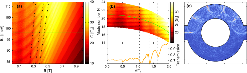
We present the conductance of the system as a function of the homogeneous magnetic field and the Fermi energy in Fig. 7(a). We observe multiple lines of local minima in this plot. In order to investigate their origin, we have replotted the data again in Fig. 7(b) with different axis. On one axis, we have placed a semiclassical approximation for the number of modes in a graphene ribbon of the width of the lead that connects to the ring (also equal to the width of the ring ). The number of modes is evaluated as a function of the two geometric scales in the setup, the magnetic length and the Fermi wavenumber and is given by
| (1) |
The expression is obtained using the translational symmetry of the problem to reduce it to one dimension and then using WKB for an approximate solution. semiribbon On the other axis we have used the inverse cyclotron radius in units of the inverse width of the geometry.
With the new axes, there are horizontal lines as well as vertical dips visible. We attribute the horizontal features to conductance quantization as they occur where the appearance of a new mode is expected in a plain graphene ribbon. The vertical features are more intriguing and are the main focus of this section. They occur at a fixed ratios of the cyclotron orbit with respect to the geometry of the ring. Therefore, it seems likely that they are connected to magnetic focusing due to the bending of the classical trajectories of the electrons in a magnetic field.houten
In order to test this hypothesis, we have performed a set of classical simulations of the transport through the ring. We have traced the path of individual trajectories propagating through the geometry assuming specular reflection at the boundary. With each trajectory starting from a random initial condition in the lead that is propagating toward the ring. We evaluated in a Monte-Carlo scheme the fraction of trajectories that propagate through the ring. In order to compare the findings with the quantum results we evaluated , with being the semiclassical number of modes as in Eq. (1).
Comparing the position of the vertical dips with the dips in the transmission probability in Fig. 7(b), we observe a correspondence for . Note that when keeping the Fermi energy constant, we follow a bent curve (e.g., the solid green line for meV) and thus in traces we can see both the horizontal as well as the vertical features.
Fig. 7(c) displays the electron density of a specific mode that is incoming from the left lead. The maximum of the density follows semicircular paths that correspond to classical cyclotron orbits. The ratio of the cyclotron radius and the dimension of the geometry is chosen such that after four (almost specular) reflections at the upper part of the outer radius, the electron enters the right lead. Such a mode contributes to transport with a conductance close to the maximal value . Increasing the magnetic field slightly decreases the cyclotron radius such that at some point there will be a reflection right before entering the right lead and the trajectory of the electron subsequently skipping over the right lead. Here, the probability for entering the right lead is heavily lowered which results in a reduction of the conductance. As a result the conductance oscillates as a function of the magnetic field. This is the reason for the magnetic focusing shown in Fig. 7(c).
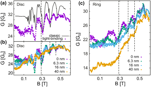
In Fig. 8(a), we have performed a more detailed comparison for a simpler setup of a graphene disk with . The idea is that the inner radius is not important at all for the occurrence of the effect. In particular, no well-defined trajectories imposed by the constriction are required as in the case for Aharonov-Bohm oscillations. The results of the simulation are in good agreement. In particular, the classical prediction for the transmission probability matches the results form the tight-binding calculation rather well up to the value where the quantum Hall effect evolves. For small cyclotron radii with there is essentially no difference between ring and disk geometry since the number of trajectories touching the inner boundary gets significantly reduced.
The conductance oscillations due to the magnetic focusing are easily distinguishable from universal conductance fluctuations. The magnitude is larger than a conductance quantum as multiple modes simultaneously fulfill the focusing condition.
The effect is only dependent on the cyclotron radius and the device geometry. For an estimation of the thermal stability, we compare the magnitude of the thermal fluctuations of the cyclotron radius with the width of the ring arm . For the experimental parameters (1 T and K), we obtain the estimate nm which is orders of magnitude smaller than .
A.3 Edge roughness
After modeling the basics of magnetic focusing, we concentrate now on the extension of the simulation for a better accordance to the experimental findings. In the experiment no quantized conductance is observed (horizontal features) and the oscillations due to magnetic focusing appear as plateaus in the magnetoconductance (compare Fig. 4(e)) Different from the experimental situation, we have considered a perfect graphene ring without any disorder and edge roughness so far. From the large mobility measured in the system, we conclude that impurity scattering is negligible in the bulk of the device. Therefore, we attribute the difference between the experimental data and the simulation to edge roughness at the graphene boundaries. For a simple model of edge roughness, we modulate the radius of the outer ring with and variable amplitude .inner Note that we do not intend to realistically model the edge roughness of the experimental situation. One of the reason is that the chemistry at the edge is not sufficiently understood. But even more importantly, as we simulate a scaled version of the graphene lattice, edge defects that appear on the scale of single atoms cannot be included even in principle. As a result, we model the edge roughness by a single effective parameter in the simple model given above. Figure 8(b) shows the effect of the edge roughness on the magnetic focusing in the disk geometry. As it is evident from the plot, the features due to magnetic focusing are rather robust toward the inclusion of edge roughness.
Fig. 8(c) makes the connection to the experiment as it displays the situation of a graphene ring with the effect of edge roughness taken into account. We see that increasing the edge roughness from to nm starts suppressing the features of quantization and magnetic focusing. At an edge-roughness of about nm the features are transformed to a more shoulder-like behavior (e.g., between the two vertical dashed lines). The experimental situation is best described with this level of edge disorder.note1
References
- (1) See e.g.: Y. Imry, “Introduction to mesoscopic physics”, Oxford University Press (2002).
- (2) P. A. Lee, and A. D. Stone, Phys. Rev. Lett. 55, 1622 (1985).
- (3) B. J. van Wees, H. van Houten, C. W. J. Beenakker, J. G. Williamson, L. P. Kouwenhoven, D. van der Marel, and C. T. Foxon, Phys. Rev. Lett. 60, 848 (1988).
- (4) A. C. Bleszynski-Jayich, W. E. Shanks, B. Peaudecerf, E. Ginossar, F. von Oppen, L. Glazman, J. G. E. Harris, Science 326, 272 (2009).
- (5) R. A. Webb, S. Washburn, C. P. Umbach and R. B. Laibowitz, Phys. Rev. Lett. 54, 2696 (1985).
- (6) A. K. Geim and I. V. Grigorieva, Nature 499, 419 (2013).
- (7) L. Banszerus, M. Schmitz, S. Engels, M. Goldsche, K. Watanabe, T. Taniguchi, B. Beschoten, and C. Stampfer, Nano Lett. 16, 1387 (2016).
- (8) P. Boggild, J. M. Caridad, C. Stampfer, G. Calogero, N. R. Papior, and M. Brandbyge, Nat. Commun. 8, 15783 (2017).
- (9) For a review see: N. Agrawal, S. Ghosh, and M. Sharma, Int. J. Mod. Phys. B 27, 1341003 (2013).
- (10) A. F. Young and P. Kim, Nat. Phys. 5, 222 (2009).
- (11) C. Handschin, P. Makk, P. Rickhaus, M.-H. Liu, K. Watanabe, T. Taniguchi, K. Richter, and C. Schönenberger, Nano Lett. 17, 328 (2017).
- (12) T. Taychatanapat, K. Watanabe, T. Taniguchi and P. Jarillo-Herrero, Nat. Phys. 9, 225-229 (2013).
- (13) G.-H. Lee, G.-H. Park and H.-J. Lee, Nat. Phys. 11, 925 (2015).
- (14) Q. Wilmart, S. Berrada, D. Torrin, V H. Nguyen, G. Fève, J.-M. Berroir, P. Dollfus and B. Plaçais, 2D Materials 1, 011006 (2014).
- (15) I. V. Borzenets, F. Amet, C. T. Ke, A. W. Draelos, M. T. Wei, A. Seredinski, K. Watanabe, T. Taniguchi, Y. Bomze, M. Yamamoto, S. Tarucha, and G. Finkelstein, Phys. Rev. Lett. 117, 237002 (2016).
- (16) Y. Aharonov, D. Bohm, Phys. Rev. 3, 485 (1959).
- (17) G. Timp, A. M. Chang, J. E. Cunningham, T. Y. Chang, P. Mankiewich, R. Behringer and R. E. Howard, Phys. Rev. Lett. 58, 2814 (1987).
- (18) S. Russo, J. B. Oostinga, D. Wehenkel, H. B. Heersche, S. S. Sobhani, L. M. K. Vandersypen and A. F. Morpurgo, Phys. Rev. Lett. 77, 085413 (2008).
- (19) M. Huefner, F. Molitor, A. Jacobsen, A. Pioda, C. Stampfer, K. Ensslin, and T. Ihn, Phys. Status Solidi (b) 246, 2756 (2009).
- (20) M. Huefner, F. Molitor, A. Jacobsen, A. Pioda, C. Stampfer, K. Ensslin and T. Ihn, New J. Phys. 12, 043054 (2010).
- (21) D. Smirnov, H. Schmidt, and R. J. Haug, Appl. Phys. Lett. 100, 203114 (2012).
- (22) D. Cabosart, S. Faniel, F. Martins, B. Brun, A. Felten, V. and B. Hackens, Phys. Rev. B 90, 205433 (2014).
- (23) C. Stampfer, J. Güttinger, S. Hellmüller, F. Molitor, K. Ensslin, and T. Ihn, Phys. Rev. Lett. 102, 056403 (2009).
- (24) P. Gallagher, K. Todd, Kathryn and D. Goldhaber-Gordon, Phys. Rev. B 81, 115409 (2010).
- (25) C. R. Dean, A. F. Young, I. Meric, C. Lee, L. Wang, S. Sorgenfrei, K. Watanabe, T. Taniguchi, P. Kim, K. L. Shepard and J. Hone, Nat. Nanotechnol. 5, 722 (2010).
- (26) A. S. Mayorov, R. V. Gorbachev, S. V. Morozov, L. Britnell, R. Jalil, L. A. Ponomarenko, P. Blake, K. S. Novoselov, K. Watanabe, T. Taniguchi and A. K. Geim, Nano Lett. 11, 2396 (2011).
- (27) L. A. Ponomarenko, A. K. Geim, A. A. Zhukov, R. Jalil, S. V. Morozov, K. S. Novoselov, I. V. Grigorieva, E. H. Hill, V. V. Cheianov, V. I. Fal’ko, K. Watanabe, T. Taniguchi and R. V. Gorbachev, Nat. Phys 7, 958 (2011).
- (28) L. Wang, I. Meric, P. Y. Huang, Q. Gao, Y. Gao, H.Tran, T. Taniguchi, K. Watanabe, L. M. Campos, D. A. Muller, J. Guo, P. Kim, J. Hone, K. L. Shepard and C. R. Dean, Science 342, 614 (2013).
- (29) B. Terrés, L. A. Chizhova, F. Libisch, J. Peiro, D. Jörger, S. Engels, A. Girschik, K. Watanabe, T. Taniguchi, S. V. Rotkin, J. Burgdörfer, and C. Stampfer, Nat. Commun. 7, 11528 (2016).
- (30) S. Engels, A. Epping, C. Volk, S. Korte, B. Voigtländer, K. Watanabe, T. Taniguchi, S. Trellenkamp, and C. Stampfer, Appl. Phys. Lett. 103, 073113 (2013).
- (31) D. Bischoff, A. Varlet, P. Simonet, M. Eich, H. C. Overweg, T. Ihn, and K. Ensslin, Appl. Phys. Rev. 2, 031301 (2015).
- (32) C. Groth, M. Wimmer, A. Akhmerov and X. Waintal, New J. Phys. 16, 063065 (2014).
- (33) From the SFM image we extract a 4W path length of m and with accounting twice the ring width nm for path width we estimate the aspect ratio .
- (34) The mean free path is calculated as a lower and an upper estimate for V and cm2/Vs.
- (35) For more details see: N. J. G. Couto, D. Costanzo, S. Engels, D.-K. Ki, K. Watanabe, T. Taniguchi, C. Stampfer, F. Guinea and A. F. Morpurgo, Phys. Rev. X 4, 041019 (2014).
- (36) D. A. Abanin and L. S. Levitov, Phys. Rev. B 78, 035416 (2008).
- (37) The periodicity of AB oscillations can be determine by the sample geometry , where the radius is set to nm, nm and nm, respectively.
- (38) We define visibility as the ratio of AB amplitude and the 2W conductance at zero magnetic field .
- (39) P. Vasilopoulos, O. Kéalméan, F. M. Peeters and M. G. Benedict, Phys. Rev. B 75, 035304 (2007).
- (40) C. J. B. Ford, T. J. Thornton, R. Newbury, M. Pepper, H. Ahmed, D. C. Peacock, D. A. Ritchie, J. E. F. Frost and G. A. C. Jones, Appl. Phys. Lett. 54, 21 (1988).
- (41) A. E. Hansen, A. Kristensen, S. Pedersen, C. B. Sorensen and P. E. Lindelof, Phys. Rev. B 64, 045327 (2001).
- (42) B. Grbić, R. Leturcq, T. Ihn, K. Ensslin, D. Reuter and A. D. Wieck, Phys. Rev. Lett. 99, 176803 (2007).
- (43) L. C. Mur, C. J. P. M. Harmans and W. G. van der Wiel, New J. Phys. 10, 073031 (2008).
- (44) C. W. J. Beenakker and H. van Houten, in Solid State Physics, edited by H. Ehrenreich and D. Turnbull, Academic, New York (1991).
- (45) D.-K. Ki and A. F. Morpurgo, Phys. Rev. Lett. 108, 266601 (2012).
- (46) J. Martin, N. Akerman, G. Ulbricht, T. Lohmann, J. H. Smet, K. von Klitzing and A. Yacoby, Nat. Phys. 4, 144 (2007).
- (47) J. Xue, J. Sanchez-Yamagishi, D. Bulmash, P. Jacquod, A. Deshpande, K. Watanabe, T. Taniguchi, P. Jarillo-Herrero and B. J. LeRoy, Nature Mat. 10, 282 (2011).
- (48) Forschungszentrum Jülich GmbH. HNF - Helmholtz Nano Facility. Journal of large-scale research facilities, 3, A112 (2017).
- (49) J. Wurm, M. Wimmer, H. U. Baranger and K. Richter, Semicond. Sci. Technol. 25, 034003 (2010).
- (50) G. Montambaux, Eur. Phys. J. B 79, 215 (2011).
- (51) H. van Houten and C. W. J. Beenakker, Quantum point contacts and coherent electron focusing, in Analogies in Optics and Micro Electronics, edited by W. van Haeringen and D. Lenstra (Kluwer, Dordrecht, 1990).
- (52) We only include edge roughness of the outer edge as the physics is dominated by this edge. We have checked that edge roughness on the inner edge has a negligible impact on the final results.
- (53) Moreover, we observe that the shoulder-like curve even turns on a rather monotonous behavior at higher strength of the edge disorder.