Spin precession and spin Hall effect in monolayer graphene/Pt nanostructures
Abstract
Spin Hall effects have surged as promising phenomena for spin logics operations without ferromagnets. However, the magnitude of the detected electric signals at room temperature in metallic systems has been so far underwhelming. Here, we demonstrate a two-order of magnitude enhancement of the signal in monolayer graphene/Pt devices when compared to their fully metallic counterparts. The enhancement stems in part from efficient spin injection and the large resistivity of graphene but we also observe 100% spin absorption in Pt and find an unusually large effective spin Hall angle of up to 0.15. The large spin-to-charge conversion allows us to characterise spin precession in graphene under the presence of a magnetic field. Furthermore, by developing an analytical model based on the 1D diffusive spin-transport, we demonstrate that the effective spin-relaxation time in graphene can be accurately determined using the (inverse) spin Hall effect as a means of detection. This is a necessary step to gather full understanding of the consequences of spin absorption in spin Hall devices, which is known to suppress effective spin lifetimes in both metallic and graphene systems.
I Introduction
Spin Hall effects (SHE) are a family of relativistic phenomena in which electrical currents generate transverse spin currents and vice versa as a consequence of spin-orbit coupling (SOC) Sinova et al. (2015). In non-magnetic materials, they provide a versatile tool for the generation and detection of spin currents without the insertion of ferromagnets (FMs). Early theoretical investigations showed that the SHE can be of extrinsic Dyakonov and Perel (1971); Hirsch (1999) or intrinsic Sinova et al. (2004, 2015) origin. Experimental observations have been carried out in semiconductor and metallic systems by means of optical Kato et al. (2004); Wunderlich et al. (2005), electrical Valenzuela and Tinkham (2006) and magnetization dynamics Saitoh et al. (2006) methods, triggering many fundamental studies and potential applications Jungwirth et al. (2012).
The exploration of the SHE using nonlocal (NL) measurements Valenzuela and Tinkham (2006, 2007) have been frequently performed in metals using Pt as the large SOC material Kimura et al. (2007); Vila et al. (2007). In semiconductor systems, detection and modulation of the inverse SHE (ISHE) has been achieved in n-GaAs by means of spin precession in combination with external electric fields Olejník et al. (2012). These studies have led to a better comprehension of the phenomena and more accurate determinations and control of the spin-to-charge conversion efficiency, which is quantified by the spin Hall angle (). For instance, can be enhanced by using metallic alloys Laczkowski et al. (2014); Niimi et al. (2012), or tuned by changing the electrical resistivity Sagasta et al. (2016). Moreover, recent experiments have demonstrated that spin currents generated by the SHE can be large enough to switch the magnetization of nanomagnets Miron et al. (2011); Liu et al. (2012) and induce fast domain wall motion Emori et al. (2013), highlighting the potential use of the SHE in conventional spintronic devices Liu et al. (2012) and pointing the path towards future spintronics without FMs.
Additionally, 2D materials have emerged as promising system for spintronics owing to their tuneable electronic properties. In particular, graphene is attractive for both propagating and manipulating spin information over long distances because of its long spin-diffusion length Han et al. (2014); Roche and Valenzuela (2014); Roche et al. (2015). Studies of spin relaxation in graphene has been explored using standard Hanle measurements Tombros et al. (2007); Han and Kawakami (2011); Han et al. (2010); Amamou et al. (2016); Neumann et al. (2013); Kamalakar et al. (2015); Volmer et al. (2015) and out-of-plane precession to determine the spin relaxation anisotropy Raes et al. (2016). Improvements in the graphene quality have led to in the range of tens of micrometers, which is already suitable for a number of applications Kawakami (2015); Chen et al. (2016).
Nonlocal signals detected in H-shape graphene structures decorated with metallic particles have been interpreted as due to large spin Hall effects, owing to SOC by proximity effects Balakrishnan et al. (2014). Theoretical analysis suggests that the proximity SOC should indeed enhance the spin Hall effect Ferreira et al. (2014); Van Tuan et al. (2016), but also that the signal in the H-shape structures can be affected by additional non spin-related contributions, which can lead to incorrect interpretations Van Tuan et al. (2016); Mihajlović et al. (2009). More recent experiments using a ferromagnetic source/detector in multilayer graphene/Pt spin devices demonstrated large spin signals at room temperature, showing the potential of graphene-based devices for spin to charge conversion Yan et al. (2017).
Here, we unambiguously demonstrate the observation of the (I)SHE in monolayer graphene/Pt structures. We show that the spin-dependent properties of graphene can be fully characterised by combining spin precession experiments with the ISHE. We use an established spin-sensitive method Valenzuela and Tinkham (2006) in which a spin polarised current is injected into the graphene channel by using a FM (Fig. 1a). The spin current precessing along the channel by the action of a magnetic field is then probed by measuring the resulting voltage generated by the ISHE in the Pt detector. Remarkably, the spin signals at room temperature are two orders of magnitude larger than those observed in equivalent devices with metallic channels. The spin current absorption by Pt becomes complete when the graphene is used in monolayer form, which has never been observed before. In addition, the use of highly-doped Si substrates allows us to modulate such signals by the action of a backgate voltage, providing a new tool to explore the spin relaxation dependence on the carrier density. In order to interpret the results, we develop a model to extract the spin Hall angle of Pt together with the graphene , and associated spin relaxation time , in the region where the Pt wire is inserted. We find that is typically in the range of hundreds of picoseconds, in agreement with the estimations with standard Hanle measurements Han et al. (2014). Our results therefore demonstrate a powerful method to study and characterise spin-dependent properties in non-magnetic materials, while the large signals open the door for room-temperature spintronic devices without the use of FMs.
II Device Fabrication
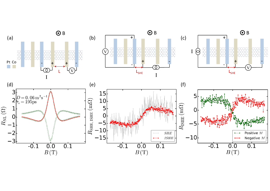
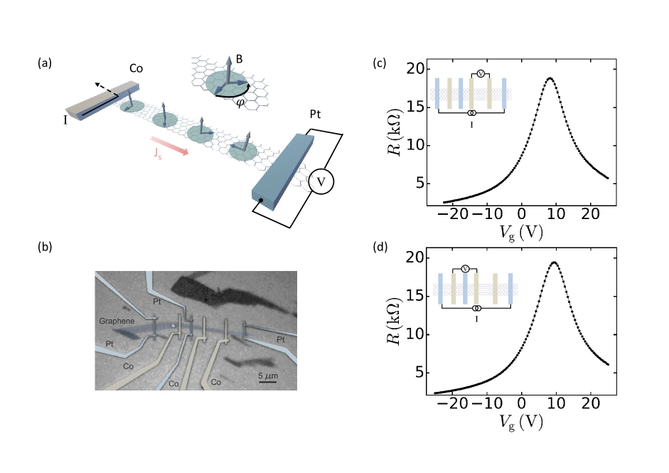
Figure 1b shows an optical micrograph of a typical device, which comprises Co and Pt electrodes connected to a graphene flake that is used as a spin channel. Graphene flakes are mechanically exfoliated from a highly oriented pyrolytic graphite source onto a p-doped Si substrate covered with 440-nm thick SiO2, which is used to control the graphene carrier density. The Pt and FM Co electrodes are defined in subsequent e-beam lithography steps and deposition in a high vacuum e-beam evaporator ( Torr). A 0.3 nm thick sticking layer of Ti is deposited prior to the deposition of Pt (12 nm thick; 150 nm wide). To assure good spin injection onto graphene 0.8 nm thick, TiO2 barriers are fabricated in a controlled oxygen environment. The 30 nm thick FM electrodes are designed with widths of 150 and 200 nm in order to vary their coercive fields and enable access to the parallel and antiparallel magnetization configurations. After fabrication the samples are inspected with optical microscopy prior to the measurements and then fully characterized with SEM after concluding the experiments. The selected graphene flakes are typically m wide and homogeneous along the device length.
III Results and discussion
Transport measurements presented hereafter have been carried out at room temperature in a vacuum environment ( Torr). The injected current varies from 1 to 5 A. Figures 1c and d display the resistance as a function of gate voltage at two different regions of the channel (the electrode configurations are shown in the insets). The first region (Fig. 1c), corresponding to the section of the channel where there is no Pt wire, is used as a reference to carry out standard Hanle measurements. The second region (Fig. 1d) corresponds to the zone where the Pt wire has been inserted in order to measure the SHE and characterize the spin absorption. It is observed that is not significantly modified by the presence of the Pt wire. In both regions graphene is weakly p-doped, with the charge neutrality point (CNP) located at V. The extracted mobility and residual carrier density are cm2(Vs)-1 and cm-2, which are comparable to those obtained in devices fabricated using angle evaporation without breaking vacuum Raes et al. (2016), demonstrating the reproducibility and quality of the device fabrication.
The spin transport is characterised by using standard non-local Hanle measurements. Here, an electrical current passing through the interface between the FM electrode and the graphene creates an out-of-equilibrium spin accumulation. Spin diffusion leads to the generation of a spin current along the channel, which is then detected by measuring the voltage at the second FM electrode (see Fig. 2a). An external magnetic field applied out of the plane of the sample induces precession therefore modulating the detected signal. Figure 2d shows obtained for the parallel and antiparallel magnetic configuration at = -20 V. The spin signal is recorded while sweeping the magnetic field down. The long channel length of 7 m, and the large Co/TiO2 interface resistance, typically between 12 k to 20 k, reduce the influence of the electrodes in the spin dynamics and help minimize the effects associated to the magneto resistance of graphene, as the magnetic field required for the complete characterisation of spin precession is small Raes et al. (2016). As observed in Fig. 2d, average and spin precession angles are achieved at relatively low mT (zero crossing) and mT (minima), respectively.
The output voltage under the influence of can be modeled considering the diffusion of carriers in one dimension by Tombros et al. (2007),
| (1) |
where , , and are the effective spin polarization of the FM electrodes, the electron charge, the density of states and the width of graphene, respectively. is the distribution function for electrons at the injector to reach the detector in time while describes the spin relaxation in the channel. is equal to , with the spin diffusion constant and the distance between injector and detector. The contribution of a carrier to is proportional to the projection of the spin along the direction of the electrode magnetization, with the Larmor frequency. As observed in Fig. 2d, the experimental results are in good agreement with Eq. (1) (red curve), allowing us to extract the graphene spin dependent parameters, m, and m2s-1, which compare well with typical values obtained in graphene-based nonlocal devices on a Si/SiO2 substrate Han et al. (2014). Assuming equal polarization at both interfaces, the effective spin polarisation of the electrodes is .
Having characterised the devices with conventional Hanle experiments we carry out the measurements based on the ISHE using the probe configuration shown in Fig. 2b. A current is injected at a FM electrode, which generates a spin current flowing towards Pt. As in the previous measurements, the external magnetic field is applied perpendicular to the graphene plane to induce spin precession. The spin current is then absorbed at the Pt/graphene interface, resulting in a voltage , and the corresponding spin Hall resistance , due to the ISHE in Pt (red curve in Fig. 2e). We observe that is antisymmetric with . At low , is approximately linear, whereas at higher , reaches a maximum and then decreases. Such a behavior is expected from a spin-related signal. Indeed, is proportional to the cross product () between the spin current and the spin orientation Hirsch (1999); Sinova et al. (2015). Because the magnetization of the FM electrodes is oriented along their length, the spins at are parallel to the Pt wire and is zero. Only when a non-zero magnetic field is applied, the spins are detected, as spin precession generates a spin component perpendicular to the Pt wire. When increases, reaches a maximum and then decreases as the average spin precession angle exceeds . The decrease of the signal at large ( mT) is associated to spin dephasing. In contrast to the standard SHE detection Valenzuela and Tinkham (2006); Kimura et al. (2007); Vila et al. (2007); Laczkowski et al. (2014); Niimi et al. (2012); Sagasta et al. (2016), the FM electrodes do not rotate as the magnetic field is swept, therefore the signal is not saturated to a finite value and approaches zero instead.
As discussed previously, in the ISHE measurement the spin current injected into graphene is detected by measuring the resulting , and associated , in the Pt wire. In the direct SHE, the spin current is injected into graphene by passing an electrical current in the Pt wire. It is then detected by measuring the voltage between the FM electrode and the Pt wire located far from the injection point, from which the spin Hall resistance is obtained. Figure 2e demonstrates that , as expected from the Onsager symmetry relations Sinova et al. (2015); Valenzuela and Tinkham (2006, 2007); Kimura et al. (2007).
An additional confirmation of the spin-related origin of the signal is shown in Fig. 2f. Here, is recorded before and after the magnetization of the injector is reversed with an in-plane magnetic field. Because the spin Hall voltage is proportional to , changing the orientation of the magnetization of the injector, and thus of the injected spins, directly modifies the detected voltage. As expected from a signal generated by spin currents, reversing the magnetization results in an inverted .
Remarkably, the signal magnitude in our devices based on monolayer graphene can exceed 10 m, which is two orders of magnitude larger than the maximum reported value in metallic systems, even at cryogenic temperatures Laczkowski et al. (2014); Niimi et al. (2012); Sagasta et al. (2016). Such an increase is crucial to fully characterise the spin precession and determine the spin-dependent parameters in these type of structures at room temperature. The enhancement in comparison with metallic systems originates from the large spin injection achieved with resistive barriers and the reduction of the current shunting through the channel. Indeed, SHE detection using tunnel barriers has only been implemented using Al as a spin channel Valenzuela and Tinkham (2006), where the high spin polarisation () and efficient spin injection permitted the determination of the spin Hall angle of Al [], which is two to three order of magnitude smaller than typical values reported for Pt Sinova et al. (2015). Direct verification of the improved spin injection in our system has been done by calculating the spin current density at the injection point and comparing it with metallic systems. The current shunting through the channel is strongly reduced because the spin resistance of graphene [ k] is much larger than the one of platinum [ ]. This feature can be important for an accurate extraction of the spin Hall angle since here all the current contributes to the ISHE signal, which is not the case for metallic systems. Note that the distance from the Hall cross to the injector is chosen so that significant precession is achieved at moderate ; larger by a factor two or more can easily be achieved by reducing such a distance, as it is done in metallic systems.
In order to quantitatively describe the results in Fig. 2, we develop a model based on one-dimensional diffusion equations in analogy to the model used for spin accumulation at a remote FM detector (Eq. 1). Assuming that the spin current in Pt flows perpendicular to the Pt/graphene interface, the resulting can be expressed as:
| (2) |
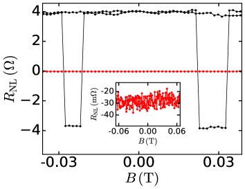
where , , , and are the electrical resistivity, spin relaxation length, thickness, width and spin Hall angle of Pt, respectively. Equation 2 is derived by assuming complete absorption of the spin current in the Pt wire, as described in the supplementary information. This assumption is supported by spin absorption experiments by measuring the spin signal in a nonlocal spin device with the Pt wire inserted between the spin injection and detection electrodes. As observed in Fig. 3, we find a completely flat versus in plane magnetic field. As a comparison, the spin signal of a reference device with no inserted Pt wire is also shown. Considering the noise level as an upper bound for the change in in the zone where Pt is inserted, its values is m. It is almost three orders of magnitude smaller than the value found in the reference device, .
Equation 2 mainly differs from the standard Hanle result, Eq. 1, in the sinusoidal dependence on in the integrand, which originates from the cross product. The sine factor is responsible of the antisymmetric behaviour of versus observed in the experiments, as well as the extrema at the average precession of .
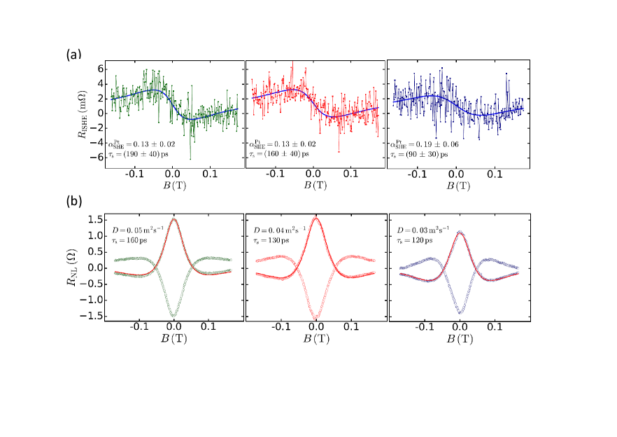
The spin relaxation time of graphene and the spin Hall angle of Pt can now be determined by fitting the experimental data using Eq. 2. To this end, the spin diffusion constant and effective spin polarisation values are extracted from the standard Hanle analysis in the same device (shown in Fig. 2d). The values of cm, nm, nm and m are all measured, whereas only nm is taken from the literature, roughly corresponding to the average value at room temperature for Pt with similar resistivity Sinova et al. (2015). With these assumptions, we obtain ps, which is in good agreement with the value from the standard Hanle analysis, ps. Because the spin precession lineshape is identical to that when spin absorption is not taken into account, this verifies that the effective is not significantly affected by spin absorption Han et al. (2010) (see supplementary information).
Interestingly, is significantly larger than the largest values reported in metallic systems with comparable , , and close to the assumed values in multilayer graphene/Pt structures Yan et al. (2017), which were not measured but extrapolated from the results obtained in low resistivity Pt Sagasta et al. (2016). However, the resistivity of Pt in our device is significantly smaller than that in Yan et al. (2017), cm, and thus the large is unexpected Sagasta et al. (2016).
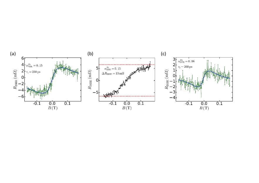
In order to go beyond this analysis and confirm our results, we perform complementary experiments using the standard SHE detection Valenzuela and Tinkham (2006); Vila et al. (2007) and investigate the carrier density dependence of in additional devices. The standard SHE detection consists of using the probe configuration shown in Fig. 2b with an in-plane magnetic field along the channel axis. In this configuration, follows a linear dependence at low magnetic field, which results from the dependence on the rotation angle of the FM towards Valenzuela and Tinkham (2006). At large enough , saturates when the magnetization rotates and is parallel to . The results are shown in Fig. 4b and demonstrate that saturation is reached at mT. The extracted spin Hall angle with this approach is , which is in excellent agreement with the previous analysis.
Figures 4c and 5 display vs in devices two and three respectively. Device two is fabricated in a different region of the graphene flake used for the device in the prior discussion. Experimental results are shown in Fig. 4c. The magnitude of is smaller than in, for example, Fig. 4a because of the longer graphene channel m. Using Eq. 2 results in ps, which is in good agreement with the values obtained from the standard Hanle analysis ps. The extracted spin Hall angle is . Figure 5 shows the spin Hall and corresponding Hanle measurements for a third device, where m. The measurements are carried out at the indicated gate voltages to show their carrier-density dependence. is observed to reach a minimum at the CNP, as commonly found in standard Hanle measurements. The diminution of as Vg approaches the CNP is due to the decrease in combined with the conductivity mismatch effect expected for pinhole-like barriers and transparent interfaces, where the signal scales with the conductivity of the channel Han et al. (2010). Using Eqs. 1 and 2 for the Hanle and spin Hall measurements, respectively, confirms the equivalence between the approaches to obtain . The extracted spin Hall angles are for V, for V and for V, which within the uncertainty of our measurements is gate independent. The estimated obtained in three different devices is therefore in the range of 0.08-0.15.
To calculate , we have taken the geometric mean of the polarization of two ferromagnetic electrodes to estimate , and have assumed nm, which is roughly the average of the values found in the literature Sinova et al. (2015). If was larger than 5 nm, would be somewhat overestimated by a few percentage points. However, recent experiments report values that are lower than 5 nm for the resistivity of our Pt films Sagasta et al. (2016). If we take = 1 nm, would be underestimated by more than a factor 2. A larger of the injector electrode would lead to an overestimated , however, this is unlikely because in all our devices consistently lies between 0.12-0.16. Furthermore, 5 samples have been measured and from all of them we extract a large . In addition, our model considers that the spin current that arrives to Pt is fully absorbed by it. The lack of spin signal in the control spin absorption experiments (Fig. 3) validates this assumption. In any case, interface-driven spin relaxation or spin current flowing into the graphene towards the detector would make the actual spin current in Pt smaller, again underestimating . Therefore, our results suggest that is larger than that observed in metallic systems with comparable Pt resistivities.
IV Conclusions
A two-order of magnitude enhancement of the spin Hall signal in graphene/Pt devices is observed when compared with their fully metallic counterparts. The enhanced signal allows us to characterise spin precession in graphene under the presence of a magnetic field. By developing an analytical model based on the 1D diffusive spin-transport, we demonstrate that the effective spin relaxation time in graphene can be accurately extracted using the (inverse) spin Hall effect as a means of detection. Good agreement is observed with the spin relaxation times obtained with standard Hanle measurements, based on the detection of spin accumulation away from Pt. This is relevant since a change in the spin relaxation is typically not taken into account in the standard spin Hall experiments Vila et al. (2007), where the spin lifetimes are assumed from control experiments.
The enhanced spin Hall signal is due to the efficient spin injection into graphene in combination with a current shunting suppression and a consistently large spin-to-charge conversion, as reflected in the large spin Hall angle. In multilayer graphene /Pt devices, a similar enhancement was attributed to the suppressed shunting and the long spin relaxation length of multilayer graphene, relative to that in metallic channels Yan et al. (2017). However, the change in spin relaxation length can be overcome with suitable device design by simply adapting the spin channel length . Indeed, devices with metallic systems are designed to have m, which is of the same order of magnitude that, for example, the room-temperature spin relaxation length of Cu, a common material used for nonlocal spin Hall detection Sinova et al. (2015). Because in our devices , the longer spin relaxation length of graphene cannot play a central role. The shunting effect is very sensitive to geometrical dimensions. Typical values of the shunting reduction factor for the devices with the largest spin-to-charge conversion are about 0.2-0.3 Sinova et al. (2015); Niimi et al. (2012), thus current shunting can account for a factor 3 to 5 when comparing with those devices. Finally, our experiments show that the spin Hall angle significantly exceeds those obtained in fully metallic systems, which could indicate the presence of interfacial spin-orbit effects between graphene and Pt that are not taken into account in our analysis. Indeed, a significant modification of the spin structure and an enhanced induced spin-orbit splitting of the graphene on Pt were recently reported Klimovskikh et al. (2014). However, further experiments are required to establish the presence of interfacial effects, in particular to address sample to sample variability associated to the effective polarization of the ferromagnetic electrodes and the dependence of the spin Hall angle with the Pt thickness.
V Acknowledgments
This research was supported by the European Union’s Horizon 2020 research and innovation programme under grant agreement No. 696656, by the European Research Council under Grant Agreement No. 308023 SPINBOUND, by the Spanish Ministry of Economy and Competitiveness, MINECO (under Contracts No. MAT2013-46785-P, No MAT2016-75952-R and Severo Ochoa No. SEV-2013-0295), and by the CERCA Programme and the Secretariat for Universities and Research, Knowledge Department of the Generalitat de Catalunya 2014SGR56. J.F.S. acknowledges support from the MINECO Juan de la Cierva programme and F.B. and M.V.C from the MINECO Ramón y Cajal programme.
References
- Sinova et al. (2015) J. Sinova, S. O. Valenzuela, J. Wunderlich, C. H. Back, and T. Jungwirth, Reviews of Modern Physics 87, 1213 (2015).
- Dyakonov and Perel (1971) M. I. Dyakonov and V. I. Perel, Physics Letters A 35, 459 (1971).
- Hirsch (1999) J. E. Hirsch, Physical Review Letters 83, 1834 (1999).
- Sinova et al. (2004) J. Sinova, D. Culcer, Q. Niu, N. A. Sinitsyn, T. Jungwirth, and A. H. MacDonald, Physical Review Letters 92, 126603 (2004).
- Kato et al. (2004) Y. K. Kato, R. C. Myers, A. C. Gossard, and D. D. Awschalom, Science 306, 1910 (2004).
- Wunderlich et al. (2005) J. Wunderlich, B. Kaestner, J. Sinova, and T. Jungwirth, Physical Review Letters 94, 047204 (2005).
- Valenzuela and Tinkham (2006) S. O. Valenzuela and M. Tinkham, Nature 442, 176 (2006).
- Saitoh et al. (2006) E. Saitoh, M. Ueda, H. Miyajima, and G. Tatara, Applied Physics Letters 88, 182509 (2006).
- Jungwirth et al. (2012) T. Jungwirth, J. Wunderlich, and K. Olejník, Nature Materials 11, 382 (2012).
- Valenzuela and Tinkham (2007) S. O. Valenzuela and M. Tinkham, J. Appl. Phys. 101, 09B103 (2007).
- Kimura et al. (2007) T. Kimura, Y. Otani, T. Sato, S. Takahashi, and S. Maekawa, Physical Review Letters 98, 156601 (2007).
- Vila et al. (2007) L. Vila, T. Kimura, and Y. Otani, Physical Review Letters 99, 226604 (2007).
- Olejník et al. (2012) K. Olejník, J. Wunderlich, A. C. Irvine, R. P. Campion, V. P. Amin, J. Sinova, and T. Jungwirth, Physical Review Letters 109, 076601 (2012).
- Laczkowski et al. (2014) P. Laczkowski, J.-C. Rojas-Sánchez, W. Savero-Torres, H. Jaffrès, N. Reyren, C. Deranlot, L. Notin, C. Beigné, A. Marty, J.-P. Attané, et al., Applied Physics Letters 104, 142403 (2014).
- Niimi et al. (2012) Y. Niimi, Y. Kawanishi, D. Wei, C. Deranlot, H. X. Yang, M. Chshiev, T. Valet, A. Fert, and Y. Otani, Physical Review Letters 109, 156602 (2012).
- Sagasta et al. (2016) E. Sagasta, Y. Omori, M. Isasa, M. Gradhand, L. E. Hueso, Y. Niimi, Y. Otani, and F. Casanova, Physical Review B 94, 060412 (2016).
- Miron et al. (2011) I. M. Miron, K. Garello, G. Gaudin, P.-J. Zermatten, M. V. Costache, S. Auffret, S. Bandiera, B. Rodmacq, A. Schuhl, and P. Gambardella, Nature 476, 189 (2011).
- Liu et al. (2012) L. Liu, C.-F. Pai, Y. Li, H. W. Tseng, D. C. Ralph, and R. A. Buhrman, Science 336, 555 (2012).
- Emori et al. (2013) S. Emori, U. Bauer, S.-M. Ahn, E. Martinez, and G. S. D. Beach, Nature Materials 12, 611 (2013).
- Han et al. (2014) W. Han, R. K. Kawakami, M. Gmitra, and J. Fabian, Nature Nanotechnology 9, 794 (2014).
- Roche and Valenzuela (2014) S. Roche and S. O. Valenzuela, J. Phys. D: Appl. Phys. 47, 094011 (2014).
- Roche et al. (2015) S. Roche, J. Åkerman, B. Beschoten, J.-C. Charlier, M. Chshiev, S. P. Dash, B. Dlubak, J. Fabian, A. Fert, M. Guimarães, et al., 2D Materials 2, 030202 (2015).
- Tombros et al. (2007) N. Tombros, C. Jozsa, M. Popinciuc, H. T. Jonkman, and B. J. Van Wees, Nature 448, 571 (2007).
- Han and Kawakami (2011) W. Han and R. K. Kawakami, Physical Review Letters 107, 047207 (2011).
- Han et al. (2010) W. Han, K. Pi, K. M. McCreary, Y. Li, J. J. Wong, A. G. Swartz, and R. K. Kawakami, Physical Review Letters 105, 167202 (2010).
- Amamou et al. (2016) W. Amamou, Z. Lin, J. van Baren, S. Turkyilmaz, J. Shi, and R. K. Kawakami, APL Materials 4, 032503 (2016).
- Neumann et al. (2013) I. Neumann, J. Van de Vondel, G. Bridoux, M. V. Costache, F. Alzina, C. M. S. Torres, and S. O. Valenzuela, Small 9, 156 (2013).
- Kamalakar et al. (2015) M. V. Kamalakar, C. Groenveld, A. Dankert, and S. P. Dash, Nature Communications 6 (2015).
- Volmer et al. (2015) F. Volmer, M. Drögeler, T. Pohlmann, G. Güntherodt, C. Stampfer, and B. Beschoten, 2D Materials 2, 024001 (2015).
- Raes et al. (2016) B. Raes, J. E. Scheerder, M. V. Costache, F. Bonell, J. F. Sierra, J. Cuppens, J. Van de Vondel, and S. O. Valenzuela, Nature Communications 7, 11444 (2016).
- Kawakami (2015) R. Kawakami, 2D Materials 2, 034001 (2015).
- Chen et al. (2016) F. W. Chen, H. Ilatikhameneh, G. Klimeck, Z. Chen, and R. Rahman, IEEE Journal of the Electron Devices Society 4, 124 (2016).
- Balakrishnan et al. (2014) J. Balakrishnan, G. K. W. Koon, A. Avsar, Y. Ho, J. H. Lee, M. Jaiswal, S.-J. Baeck, J.-H. Ahn, A. Ferreira, M. A. Cazalilla, et al., Nature Communications 5, 4748 (2014).
- Ferreira et al. (2014) A. Ferreira, T. Rappoport, M. Cazalilla, and A. Neto, Physical Review Letters 112, 066601 (2014).
- Van Tuan et al. (2016) D. Van Tuan, J. M. Marmolejo-Tejada, X. Waintal, B. K. Nikolić, S. O. Valenzuela, and S. Roche, Physical Review Letters 117, 176602 (2016).
- Mihajlović et al. (2009) G. Mihajlović, J. E. Pearson, M. A. Garcia, S. D. Bader, and A. Hoffmann, Physical Review Letters 103, 166601 (2009).
- Yan et al. (2017) W. Yan, E. Sagasta, M. Ribeiro, Y. Niimi, L. E. Hueso, and F. Casanova, arXiv preprint arXiv:1702.01971 (2017).
- Klimovskikh et al. (2014) I. I. Klimovskikh, S. S. Tsirkin, A. G. Rybkin, A. A. Rybkina, M. V. Filianina, E. V. Zhizhin, E. V. Chulkov, and A. M. Shikin, Physical Review B 90, 235431 (2014).