Complex THz and DC inverse spin Hall effect in YIG/Cu1-xIrx bilayers across a wide concentration range
Abstract
We measure the inverse spin Hall effect of Cu1-xIrx thin films on yttrium iron garnet over a wide range of Ir concentrations (). Spin currents are triggered through the spin Seebeck effect, either by a DC temperature gradient or by ultrafast optical heating of the metal layer. The spin Hall current is detected by, respectively, electrical contacts or measurement of the emitted THz radiation. With both approaches, we reveal the same Ir concentration dependence that follows a novel complex, non-monotonous behavior as compared to previous studies. For small Ir concentrations a signal minimum is observed, while a pronounced maximum appears near the equiatomic composition. We identify this behavior as originating from the interplay of different spin Hall mechanisms as well as a concentration-dependent variation of the integrated spin current density in Cu1-xIrx. The coinciding results obtained for DC and ultrafast stimuli show that the studied material allows for efficient spin-to-charge conversion even on ultrafast timescales, thus enabling a transfer of established spintronic measurement schemes into the terahertz regime.
I Introduction
Spin currents are a promising ingredient for the implementation of next-generation, energy-efficient spintronic applications. Instead of exploiting the electronic charge, transfer as well as processing of information is mediated by spin angular momentum. Crucial steps towards the realization of spintronic devices are the efficient generation, manipulation and detection of spin currents at highest speeds possible. Here, the spin Hall effect (SHE) and its inverse (ISHE) are in the focus of current research Sinova et al. (2015) as they allow for an interconversion of spin and charge currents in heavy metals with strong spin-orbit interaction (SOI). The efficiency of this conversion is quantified by the spin Hall angle .
In general, the SHE has intrinsic as well as extrinsic spin-dependent contributions. The intrinsic SHE results from a momentum-space Berry phase effect and can, amongst others, be observed in 4 and 5 transition metals Tanaka et al. (2008); Morota et al. (2011); Sinova et al. (2015). The extrinsic SHE, on the other hand, is a consequence of skew and side-jump scattering off impurities or defects Fert and Levy (2011). It occurs in (dilute) alloys of normal metals with strong SOI impurity scatterers Niimi et al. (2011, 2012); Zou et al. (2016); Ramaswamy et al. (2017), but can also be prominent in pure metals in the superclean regime Sagasta et al. (2016). As a consequence, the type of employed metals and the alloy composition are handles to adjust and maximize the SHE. Remarkably, it was recently shown that the SHE in alloys of two heavy metals (e.g. AuPt) can even exceed the SHE observed for the single alloy partners Obstbaum et al. (2016). Pioneering work within this research field covered the extrinsic SHE by skew scattering in copper-iridium alloys Niimi et al. (2011). However, previously the iridium concentration was limited to effective doping of Cu with dilute Ir. The evolution of the SHE in the alloy regime for large concentration thus remains an open question and the achievable maximum by an optimized alloying strategy is unknown.
The potential of a metal for spintronic applications (i.e. ) can be quantified by injecting a spin current and measuring the resulting charge response. This can be accomplished by, for instance, coherent spin pumping through ferromagnetic resonance Tserkovnyak et al. (2002); Mizukami et al. (2002); Saitoh et al. (2006) or the spin Seebeck effect (SSE) Bauer et al. (2012); Uchida et al. (2016). The SSE describes the generation of a magnon spin current along a temperature gradient within a magnetic material. Typically, such experiments involve a heterostructure composed of a magnetic insulator, such as yttrium iron garnet (YIG), and the ISHE metal under study [see Fig. 1(a)]. A DC temperature gradient in the YIG bulk is induced by heating the sample from one side. On the femtosecond timescale, however, a temperature difference and thus a spin current across the YIG-metal interface can be induced by heating the metal layer with an optical laser pulse [Fig. 1(b)] Agrawal et al. (2014); Schreier et al. (2016); Kimling et al. (2016); Seifert et al. (2017). This interfacial SSE has been shown to dominate the spin current in the metal on timescales below ns Agrawal et al. (2014).
For ultrafast laser excitation, the resulting sub-picosecond ISHE current leads to the emission of electromagnetic pulses at frequencies extending into the terahertz (THz) range, which can be detected by optical means Kampfrath et al. (2013). Therefore, femtosecond laser excitation offers the remarkable benefit of contact-free measurements of the ISHE current without any need of micro-structuring the sample. The all-optical generation as well as detection of ultrafast electron spin currents Kampfrath et al. (2013); Seifert et al. (2016) is a key requirement for transferring spintronic concepts into the THz range Walowski and Münzenberg (2016). So far, however, characterization of the ISHE was conducted by experiments including DC spin current signals as, for instance, the bulk SSE [Fig. 1(a)]. For the use in ultrafast applications, it thus remains to be shown whether alloying yields the same notable changes of the spin-to-charge conversion efficiency in THz interfacial SSE experiments [Fig. 1(b)] and whether alloys can provide an efficient spin-to-charge conversion even at the ultrafast timescale.
In this work, we study the compositional dependence of the ISHE in YIG/Cu1-xIrx bilayers over a wide concentration range (), exceeding the dilute doping phase investigated in previous studies Niimi et al. (2011). The ISHE response of Cu1-xIrx is measured as a function of , for which both DC bulk and THz interfacial SSE are employed. Eventually, we compare the spin-to-charge conversion efficiency in the two highly distinct regimes of DC and terahertz dynamics across a wide alloying range.
II Experiment
The YIG samples used for this study are of thickness, grown epitaxially on (111)-oriented Gd3Ga5O12 (GGG) substrates by liquid-phase-epitaxy. After cleaving the GGG/YIG into samples of dimension , Cu1-xIrx thin films (thickness ) of varying composition ( and 0.7) are deposited by multi-source magnetron sputtering. To prevent oxidation of the metal film, a Al capping layer is deposited, which, when exposed to air, forms an AlOx protection layer. For the contact-free ultrafast SSE measurements, patterning of the Cu1-xIrx films into defined nanostructures is not necessary. In the case of DC SSE measurements, the unpatterned film is contacted for the detection of the thermal voltage.
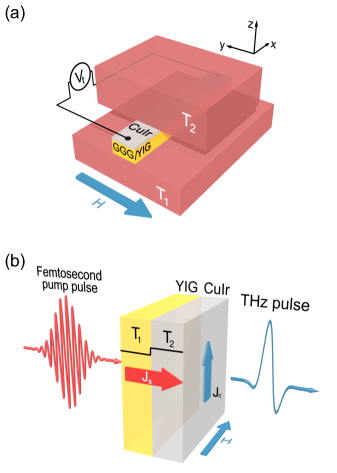
The DC SSE measurements are performed at room temperature in the conventional longitudinal configuration Uchida et al. (2016). While an external magnetic field is applied in the sample plane, two copper blocks, which can be set to individual temperatures, generate a static out-of-plane temperature gradient, see Fig. 1(a). This thermal perturbation results in a magnonic spin current in the YIG layer Kehlberger et al. (2015), thereby transferring angular momentum into the Cu1-xIrx. A spin accumulation builds up, diffuses as a pure spin current and is eventually converted into a transverse charge current by means of the ISHE, yielding a measurable voltage signal. The spin current and consequently the thermal voltage change sign when the YIG magnetization is reversed. The SSE voltage SSE is defined as the difference between the voltage signals obtained for positive and negative magnetic field divided by 2. Since SSE is the result of the continuous conversion of a steady spin current, it can, applying the notation of conventional electronics, be considered as a DC signal.
For the THz SSE measurements, the same in-plane magnetized YIG/Cu1-xIrx samples are illuminated at room temperature by femtosecond laser pulses (energy of , duration of , center wavelength of corresponding to a photon energy of , repetition rate of ) of a Ti:sapphire laser oscillator. Owing to its large bandgap of Metselaar and Larsen (1974), YIG is transparent for these laser pulses. They are, however, partially (about ) absorbed by the electrons of the Cu1-xIrx layer. The spatially step-like temperature gradient across the YIG/metal interface leads to an ultrafast spin current in the metal layer polarized parallel to the sample magnetization Seifert et al. (2017). Subsequently, this spin current is converted into a transverse sub-picosecond charge current through the ISHE, resulting in the emission of a THz electromagnetic pulse into the optical far-field. The THz electric field is sampled using a standard electrooptical detection scheme employing a thick ZnTe detection crystal Leitenstorfer et al. (1999). The magnetic response of the system is quantified by the root mean square (RMS) of half the THz signal difference for positive and negative magnetic fields.
III Results
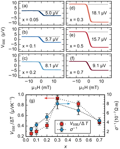
Figure 2(a)-(f) shows DC SSE hysteresis loops measured for YIG/Cu1-xIrx/AlOx multilayers with varying Ir concentration . The temperature difference between sample top and bottom is fixed to with a base temperature of . In the Cu-rich phase, we observe an increase of the thermal voltage signal with increasing , exhibiting a maximum at . Interestingly, upon further increasing the Ir content reduces again. This behavior is easily visible in Fig. 2(g), in which the SSE coefficient is plotted as a function of . The measured concentration dependence shows that exhibits a clear maximum in the range from to . Thus, as a first key result the maximum spin Hall effect is obtained for the previously neglected alloying regime beyond the dilute doping. For comparison, the resistivity of the metal film is also shown in Fig. 2(g). We see that the resistivity of the Cu1-xIrx layer follows a similar trend as the DC SSE signal.
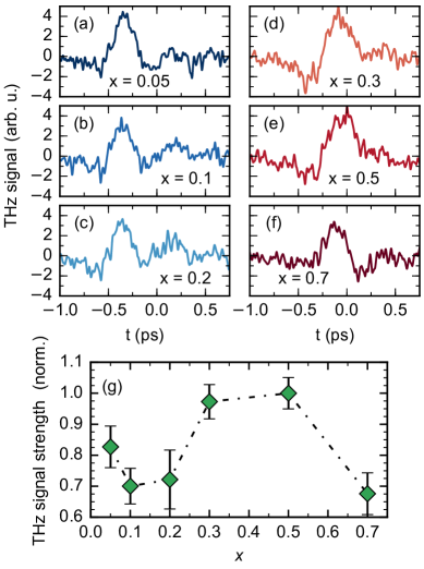
Typical THz emission signals from the YIG/Cu1-xIrx/AlOx samples are depicted in Figs. 3(a)-(f). The THz transients were low-pass filtered in the frequency domain with a Gaussian centered at zero frequency and a full width at half maximum of . The RMS of the THz signal odd in sample magnetization is plotted in Fig. 3(g) as a function of . After an initial signal drop in the Cu-rich phase, the THz signal increases with increasing Ir concentration, indicating a signal maximum in the range between and . Further increase of the Ir content leads to a second reduction of the THz signal strength.
IV Discussion
In the following, a direct comparison of the signals obtained from the DC and the ultrafast THz measurements is established. To begin with, the emitted THz electric field right behind the sample is described by a generalized Ohm’s law, which in the thin-film limit (film is much thinner than the wavelength and attenuation length of the THz wave in the sample) is in the frequency domain given by Seifert et al. (2016)
| (1) |
where is the angular frequency. The spin-current density is integrated over the full thickness of the metal film. The total impedance can be understood as the impedance of an equivalent parallel circuit comprising the metal film (Cu1-xIrx) and the surrounding substrate (GGG/YIG) and air half-spaces,
| (2) |
Here, and are the refractive indices of substrate and air, respectively, is the vacuum impedance, and is the THz sheet conductance of the Cu1-xIrx films. Considering the Drude model and a velocity relaxation rate of for pure Cu at room temperature as lower boundary Gall (2016), the values of vary only slightly over the detected frequency range from 1 to 5 THz (as given by the ZnTe detector crystal). Therefore, the frequency dependence of the conductance can be neglected, i.e. . Importantly, the metal-film conductance () is much smaller than the shunt conductance () for the investigated metal film thickness () and can be thus neglected. Therefore, the Ir-concentration influences the THz emission strength only directly through the ISHE-induced in-plane charge current flowing inside the NM layer.
The measured DC SSE voltage, on the other hand, is given by an analogous expression related to the underlying in-plane charge current by the standard Ohm’s law,
| (3) |
Here, is the Ohmic resistance of the metal layer between the electrodes, which is inversely proportional to the metal resistivity , and is the DC spin current density. Therefore, in contrast to the THz data, the impact of alloying on through is significant. For a direct comparison with the THz measurements, we thus contrast the RMS of the THz signal waveform with the DC SSE current density .
In Fig. 4, the respective amplitudes are plotted as a function of the Ir concentration. Remarkably, DC and THz SSE/ISHE measurements exhibit the very same concentration dependence. This agreement suggests that the ISHE retains its functionality from DC up to THz frequencies, which vindicates the findings and interpretations of previous experiments Seifert et al. (2016). Small discrepancies may originate from a varying optical absorptance of the near-infrared pump light, which is, however, expected to depend monotonically on and to only vary by a few percent Seifert et al. (2016). Furthermore, as discussed below, these findings imply that for DC and THz spin currents comparable concentration dependences of spin-relaxation lengths may be expected.
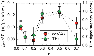
To discuss the concentration dependence of the DC and THz SSE signals (Fig. 4), we consider Eqs. (1) and (3). According to these relationships, the THz signal and the SSE voltage normalized by the metal resistivity result from a competition of (i) the spin Hall angle and (ii) the integrated spin-current density .
At first, we consider the local spin signal minimum at small, increasing Ir concentration (dilute regime) that appears for both and the THz signal. In fact, with regard to (i) one would expect the opposite behavior as for the dilute regime the skew scattering mechanism has been predicted Fert and Levy (2011) and experimentally shown Niimi et al. (2011) to yield the dominant ISHE contribution. With increasing SOI scattering center density (), a linear increase of the spin signal should appear. In this work, this trend is observed for [Fig. 2(g)]. The significantly deviating signal shapes of and the THz signal, however, suggest that the converted in-plane charge current is notably governed by additional effects. An explanation can be given by (ii), considering a spatial variation of the spin current density that, as we discuss below, can be influenced by both electron momentum- and spin-relaxation. The initial electron momenta and spin information of a directional spin current become randomized over length scales characterized by the mean free path and the spin diffusion length , yielding a reduction of the spin current density. For spin-relaxation, the integrated spin current density is given by Ando et al. (2011):
| (4) |
with being the thickness of the Cu1-xIrx layer. According to Niimi et al. Niimi et al. (2011) the spin-diffusion length decreases exponentially from for to for . This exponential decay implies that the integrated spin current density is nearly constant for both small and large , but undergoes a significant decline in the concentration region where . This effect possibly explains the observed reduction of the signal amplitude from to . Furthermore, we interpret the fact that for DC and THz SSE signals similar trends are observed as an indication of similar concentration dependences of in the distinct DC and THz regimes. This appears reasonable when considering that spin-dependent scattering rates are of the same order of magnitude as the momentum scattering Stern et al. (2008) (e.g. Gall (2016)) and thus above the experimentally covered bandwidth.
In addition to spin-relaxation, the integrated spin current density is influenced by momentum scattering. As shown in Fig. 2, alloying introduces impurities and lattice defects in the dilute phase, such that enhanced momentum scattering rates occur. Assuming that the latter increase more rapidly than , the appearance of the previously unexpected local minimum near can be thus explained.
We now focus on the subsequent increase of the spin signal at higher (concentrated phase). It can be explained by a further increase of extrinsic ISHE as well as intrinsic ISHE contributions, as pure Ir itself exhibits a sizeable intrinsic spin Hall effect Tanaka et al. (2008); Morota et al. (2011). A quantitative explanation of the intrinsic ISHE, however, requires knowledge of the electron band structure (obtainable by algorithms based on the tight-binding model Tanaka et al. (2008) or the density functional theory Guo et al. (2008)), which is beyond the scope of this work. The decrease of and the THz Signal at may then be ascribed to an increase of atomic order and thus a decrease of the extrinsic ISHE.
In conclusion, we compare the spin-to-charge conversion of steady state and THz spin currents in copper-iridium alloys as a function of the iridium concentration. We find a clear maximum of the spin Hall effect for alloys of around Ir concentration, far beyond the previously probed dilute doping regime. While the detected DC spin Seebeck voltage exhibits a concentration dependence different from the raw THz signal, very good qualitative agreement between the DC spin Seebeck current and the THz emission signal is observed, which is well understood within our model for THz emission. Ultimately, our results show that tuning the spin Hall effect by alloying delivers an unexpected, complex concentration dependence that is equal for spin-to-charge conversion at DC and THz frequencies and allows us to conclude that the large spin Hall effect in CuIr can be used for spintronic applications on ultrafast timescales.
V Acknowledgments
This work was supported by Deutsche Forschungsgemeinschaft (DFG) (SPP 1538 “Spin Caloric Transport”, SFB/TRR 173 ”SPIN+X”), the Graduate School of Excellence Materials Science in Mainz (DFG/GSC 266), and the EU projects IFOX, NMP3-LA-2012246102, INSPIN FP7-ICT-2013-X 612759, TERAMAG H2020 681917.
References
- Sinova et al. (2015) J. Sinova, S. O. Valenzuela, J. Wunderlich, C. H. Back, and T. Jungwirth, Rev. Mod. Phys. 87, 1213 (2015).
- Tanaka et al. (2008) T. Tanaka, H. Kontani, M. Naito, T. Naito, D. S. Hirashima, K. Yamada, and J. Inoue, Phys. Rev. B 77, 165117 (2008).
- Morota et al. (2011) M. Morota, Y. Niimi, K. Ohnishi, D. H. Wei, T. Tanaka, H. Kontani, T. Kimura, and Y. Otani, Phys. Rev. B 83, 174405 (2011).
- Fert and Levy (2011) A. Fert and P. M. Levy, Phys. Rev. Lett. 106, 157208 (2011).
- Niimi et al. (2011) Y. Niimi, M. Morota, D. H. Wei, C. Deranlot, M. Basletic, A. Hamzic, A. Fert, and Y. Otani, Phys. Rev. Lett. 106, 126601 (2011).
- Niimi et al. (2012) Y. Niimi, Y. Kawanishi, D. H. Wei, C. Deranlot, H. X. Yang, M. Chshiev, T. Valet, A. Fert, and Y. Otani, Phys. Rev. Lett. 109, 156602 (2012).
- Zou et al. (2016) L. K. Zou, S. H. Wang, Y. Zhang, J. R. Sun, J. W. Cai, and S. S. Kang, Phys. Rev. B 93, 014422 (2016).
- Ramaswamy et al. (2017) R. Ramaswamy, Y. Wang, M. Elyasi, M. Motapothula, T. Venkatesan, X. Qiu, and H. Yang, (2017), arXiv:1707.09525 .
- Sagasta et al. (2016) E. Sagasta, Y. Omori, M. Isasa, M. Gradhand, L. E. Hueso, Y. Niimi, Y. Otani, and F. Casanova, Phys. Rev. B 94, 060412(R) (2016).
- Obstbaum et al. (2016) M. Obstbaum, M. Decker, A. K. Greitner, M. Haertinger, T. N. G. Meier, M. Kronseder, K. Chadova, S. Wimmer, D. Ködderitzsch, H. Ebert, and C. H. Back, Phys. Rev. Lett. 117, 167204 (2016).
- Tserkovnyak et al. (2002) Y. Tserkovnyak, A. Brataas, and G. E. W. Bauer, Phys. Rev. Lett. 88, 117601 (2002).
- Mizukami et al. (2002) S. Mizukami, Y. Ando, and T. Miyazaki, Phys. Rev. B 66, 104413 (2002).
- Saitoh et al. (2006) E. Saitoh, M. Ueda, H. Miyajima, and G. Tatara, Appl. Phys. Lett. 88, 182509 (2006).
- Bauer et al. (2012) G. E. W. Bauer, E. Saitoh, and B. J. van Wees, Nat. Mater. 11, 391 (2012).
- Uchida et al. (2016) K. Uchida, H. Adachi, T. Kikkawa, A. Kirihara, M. Ishida, S. Yorozu, S. Maekawa, and E. Saitoh, P. IEEE 104, 1946 (2016).
- Agrawal et al. (2014) M. Agrawal, V. I. Vasyuchka, A. A. Serga, A. Kirihara, P. Pirro, T. Langner, M. B. Jungfleisch, A. V. Chumak, E. T. Papaioannou, and B. Hillebrands, Phys. Rev. B 89, 224414 (2014).
- Schreier et al. (2016) M. Schreier, F. Kramer, H. Huebl, S. Geprägs, R. Gross, S. T. Goennenwein, T. Noack, T. Langner, A. A. Serga, B. Hillebrands, and V. I. Vasyuchka, Physical Review B 93, 224430 (2016).
- Kimling et al. (2016) J. Kimling, G.-M. Choi, J. T. Brangham, T. Matalla-Wagner, T. Huebner, T. Kuschel, F. Yang, and D. G. Cahill, Phys. Rev. Lett. 118, 057201 (2016).
- Seifert et al. (2017) T. Seifert, S. Jaiswal, J. Barker, I. Razdolski, J. Cramer, O. Gueckstock, S. Watanabe, C. Ciccarelli, A. Melnikov, G. Jakob, S. T. B. Goennenwein, G. Woltersdorf, P. W. Brouwer, M. Wolf, M. Kläui, and T. Kampfrath, (2017), arXiv:1709.00768 .
- Kampfrath et al. (2013) T. Kampfrath, M. Battiato, P. Maldonado, G. Eilers, J. Nötzold, S. Mährlein, V. Zbarsky, F. Freimuth, Y. Mokrousov, S. Blügel, M. Wolf, I. Radu, P. M. Oppeneer, and M. Münzenberg, Nat. Nanotechnol. 8, 256 (2013).
- Seifert et al. (2016) T. Seifert, S. Jaiswal, U. Martens, J. Hannegan, L. Braun, P. Maldonado, F. Freimuth, A. Kronenberg, J. Henrizi, I. Radu, E. Beaurepaire, Y. Mokrousov, P. M. Oppeneer, M. Jourdan, G. Jakob, D. Turchinovich, L. M. Hayden, M. Wolf, M. Münzenberg, M. Kläui, and T. Kampfrath, Nat. Photonics 10, 483 (2016).
- Walowski and Münzenberg (2016) J. Walowski and M. Münzenberg, J. Appl. Phys. 120, 140901 (2016).
- Kehlberger et al. (2015) A. Kehlberger, U. Ritzmann, D. Hinzke, E.-J. Guo, J. Cramer, G. Jakob, M. C. Onbasli, D. H. Kim, C. A. Ross, M. B. Jungfleisch, B. Hillebrands, U. Nowak, and M. Kläui, Phys. Rev. Lett. 115, 096602 (2015).
- Metselaar and Larsen (1974) R. Metselaar and P. K. Larsen, Solid State Commun. 15, 291 (1974).
- Leitenstorfer et al. (1999) A. Leitenstorfer, S. Hunsche, J. Shah, M. Nuss, and W. Knox, Appl. Phys. Lett. 74, 1516 (1999).
- Gall (2016) D. Gall, J. Appl. Phys. 119, 1 (2016).
- Ando et al. (2011) K. Ando, S. Takahashi, J. Ieda, Y. Kajiwara, H. Nakayama, T. Yoshino, K. Harii, Y. Fujikawa, M. Matsuo, S. Maekawa, and E. Saitoh, J. Appl. Phys. 109, 103913 (2011).
- Stern et al. (2008) N. P. Stern, D. W. Steuerman, S. Mack, A. C. Gossard, and D. D. Awschalom, Nat. Phys. 4, 843 (2008).
- Guo et al. (2008) G. Y. Guo, S. Murakami, T. W. Chen, and N. Nagaosa, Phys. Rev. Lett. 100, 096401 (2008).