Enhanced radial growth of Mg doped GaN nanorods: A combined experiment and first-principles based analysis
Abstract
We discuss the microstructural origin of enhanced radial growth in magnesium (Mg) doped gallium nitride (GaN) nanorods (NRs) using electron microscopy and first-principles Density Functional Theory calculations. Experimentally, we find the Mg incorporation increases surface coverage of the grown samples and the height of NRs decreases as a consequence of an increase radial growth rate. We also observed the coalescence of NRs becomes prominent and the critical height of coalescence decreases with the increase in Mg concentration. From first-principles calculations, we find the surface free energy of Mg doped surface reduces with increasing Mg concentration in the samples. The calculations further suggests a reduction in the diffusion barrier of Ga adatoms along [110] on the side wall surface of the NRs, possibly the primary reason for the observed enhancement in the radial growth.
I Introduction
Free standing semiconducting nanowires (NWs) and nanorods (NRs) are promising one-dimensional nanostructures having applications in various areas such as nanoelectronics, nanophotonics, nanosensing, etcTian et al. (2007); Qian et al. (2004); Cui et al. (2001). The fundamental, as well as the advanced studies on the growth and physical properties of such nanostructures, are of great interest within the scientific communityPersson et al. (2004); Colombo et al. (2008). The effective lateral stress relaxation in the case of nanostructures originating by the presence of facet edges can minimize or sometimes eliminate the formation of dislocationsGlas (2006).Typically, these nanostructures with radii in the order of several tens of nanometers and a length of micrometers are grown using modern epitaxial growth techniques like molecular beam epitaxyDebnath et al. (2007) or metal-organic chemical vapor depositionKim et al. (2005).
III-Nitrides being an important class of semiconductors have found in many optoelectronic and microelectronic devices available today. Due to the potential integration both the technologies, the growth of GaN on Si substrates attracts much attention. Also, GaN-on-Si is also a low-cost alternative to the conventional substrates like sapphire and SiC as the Si-based technology is comparatively mature and a successful integration gives extra advantages. In this direction, the epitaxial growth of III-V compound nanostructures including GaN on Si substrates has been extensively investigatedIhn et al. (2006); Li et al. (2008); Cerutti et al. (2006). To further increase the functionalities of the grown nanostructures, doping with suitable ions is partly necessary Cui et al. (2001); Wang et al. (2005); Tang et al. (2008). It is also observed in various cases; the process of doping may result in significant changes in the morphology as the presence of impurities on surfaces can affect the dynamics of adatoms arriving on it Stamplecoskie et al. (2008); Radovanovic et al. (2007); Chen et al. (2009). Therefore, the understanding of the microstructural origin of any change in the morphology owing to the incorporation of dopants is crucial for their use in various device applications. GaN is an inherently n-doped compound semiconductor, and p-doping is a bit difficult. Out of many possible dopants, Mg is promising. Also, the Mg incorporation was also found to influence the morphology of the grown NRs strongly. A small amount of Mg can increase the tendency of the rods to coalesce while keeping their diameter unchanged without any broadening or taperingLi and Waag (2012).
Furtmayr et al. studied the effect of Mg doping on MBE grown GaN NRs and showed an increase in Mg flux results in an increase in the diameter and a decrease in their heightFurtmayr et al. (2008). The observed increase in the diameter may be because of the larger nucleation centers. However, it was concluded that the increase in the diameter of GaN NRs is due to the enhancement of the radial growth instead of larger nucleation sites. A similar increase in the radial growth in the case of Mg-GaN NRs with the increase in Mg incorporation has been reported by Zhang et al.Zhang et al. (2009) and Andrews et al.Wang et al. (2014). However, Bae et al.Bae et al. (2017) reported a variation of the height of NRs due to higher Mg flux instead of promoting vertical growth. Moreover, no convincing evidence for the origin of increased radial growth in MBE grown Mg-GaN NRs has been reported yet. Therefore, in this present work, we try to address this behavior by providing novel insights into the growth mechanism of Mg doped GaN NRs on Si by a combination of experimental and computational investigations.
II Methods
II.1 Experimental details
The GaN NRs were grown directly on Si (111) substrate under nitrogen rich conditions by a radio frequency plasma assisted molecular beam epitaxy (RF-PAMBE, SVTA-USA) system operating at a base pressure of Torr. Prior to the growth, Si (111) substrate was ultrasonically cleaned in acetone for 10 minute. Degassing of the substrate at 600 oC for 60 minute in the preparation chamber followed by degassing at 800 oC for 30 minute and at 825 oC for 5 minute in the growth chamber were carried out to get a clean Si () reconstruction. Before the growth, Si () reconstructed surface was exposed to metallic Gallium (Ga) for 10 sec. The temperature of the Ga effusion cell was maintained at 1060 oC. A constant nitrogen flow rate of 4.5 sccm (standard cubic centimeter per minute), plasma forward power of 375 W, substrate temperature of 630 oC and a growth duration of 4 hours were maintained for the growth of all samples. Mg fluxes were varied by adjusting the Mg K-cell temperature (see Table 1). The fluxes of the Mg and Ga were obtained from the beam equivalent pressure (BEP) and are tabulated in Table 1. Surface structural evolution was monitored in-situ by reflection high energy electron diffraction (RHEED) and the morphology was determined ex-situ using a field emission scanning electron microscope (FESEM, Quanta 3D operated at 20 kV). The crystal phase of the samples was determined using a high-resolution X-ray diffractometer (HR-XRD, Discover D8 Bruker) with a Cu Kα X-ray source with wavelength of 1.5406 Å. Structure of the NRs at atomic scale was studied by high resolution transmission electron microscopy (HRTEM, FEI TITAN operated at 300 kV).
| Sample | Mg K-cell | BEP | Flux | Mg:Ga |
|---|---|---|---|---|
| Name | temp (oC) | (Torr) | (atoms cm-2s-1) | |
| A | - | - | - | 0 |
| B | 340 | 0.00818 | ||
| C | 350 | 0.01127 | ||
| D | 360 | 0.01618 |
II.2 Simulation details
Ab-initio Density Functional Theory (DFT) simulations were carried to estimate the surface energy and diffusion barrier of adatoms on side wall surfaces of GaN NRs. A Generalized Gradient Approximation (GGA) of Perdew et al.Perdew et al. (1996) was used for the exchange and correlation energy functional. Integrations over the Brillouin Zone of bulk w-GaN were sampled on a -centered 553 uniform mesh of k-points in the unit cell of reciprocal spaceMonkhorst and Pack (1976). The lattice parameters and atomic co-ordinates were optimized by using conjugate gradient algorithm to minimize the energy until the forces on each atom was less than 0.04 eV/Å. Optimized lattice parameters of the unit cell of GaN are = 3.25 Å and = 5.23 Å. The surfaces (both undoped and doped) were constructed within the slab model, where 12 atomic layers in [100] direction were considered. With this model four layers of atoms in the middle were kept fixed at their bulk atomic positions to mimic the bulk configuration. We have used a vacuum of 16 Å perpendicular to (100) surface to keep the interaction between image configurations weak. In case of surface cells, a single k-point was used for the long cell direction, while for other directions, k-points were chosen to match the k-point density of the respective directions used in the bulk calculations. We have estimated surface energy of doped (100) surface by using following formula:
| (1) |
where A, Eslab, and Ebulk correspond to the surface area of the slab, the total energy of the slab, and the total energy of the bulk with same Mg concentration as slab. The diffusion barrier of the Ga adatom on undoped and doped surface were estimated from total energy calculation of respective configurations. Total energy of different configurations were estimated using SIESTA codeSoler et al. (2002).
III Results and discussion
III.1 Experimental Results
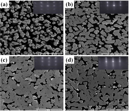
Plan view FESEM images of samples A-D grown with different Mg flux-rates (see Table 1) are shown in Fig.1. We find that most of NRs are vertically aligned with the surface of substrate while few of them are slightly tilted for undoped sample. However, for doped samples (B, C and D), we observed well aligned NRs. It is widely observed that, the relative misorientation of GaN NWs or NRs grown on Si (111) are typically about 3o, both in-plane (twist) as well as out-of-plane (tilt)Geelhaar et al. (2011); Jenichen et al. (2011); Wierzbicka et al. (2012); Fernández-Garrido et al. (2014). The RHEED pattern shown as inset of the FESEM images confirm a typical of wurtzite structure and spotty nature of it signifies a 3D morphology. However, we also observe the elongation of RHEED pattern along (100) which may due to relative misorientation of NRs with each other. The RHEED pattern of doped samples (especially C and D) show an elongated spotty pattern with faint streaky lines which are attributed to the electron scattering from the large flat c-plane tops of the NRs. A similar observation is also made by De et al. De and Shivaprasad (2016). To elucidate further, we estimate the surface coverage of samples A, B, C and D as 552%, 652%, 802% and 802% respectively suggesting an increase in the surface coverage with increasing Mg flux.
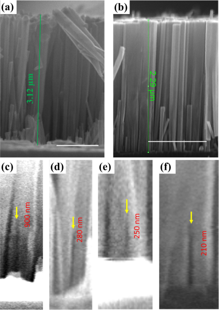
Further, to look at the interface of Si and GaN NRs, we carried out cross section FESEM imaging of samples (see Fig.2). At the early stages of growth, NRs are quite isolated but they tends to coalesce as the growth proceeds. Interestingly, we find that with an increase in the Mg flux, the critical height for coalescence of NRs is decreasing as 90010 nm, 28010 nm, 25010 nm, 21010 nm for sample A, B, C and D respectively. Kaganer et al.Kaganer et al. (2016) suggest Hc of coalescence of NRs can be calculated by
| (2) |
where E is the Young modulus, the surface energy, the width of the contact area (for the calculations, is equal to the radius of the thinner nanowire) and indicates the geometrical moments of inertia of the cross-section of the corresponding nanowire (i=1,2). For a cylinder, where is separation between nanowires at the bottom. Equation 2 suggests that, while keeping all other parameters fixed an increase in results in the reduction of . Our first-principles calculations suggest a small reduction in the surface free energy (as shown in Fig.5(c)) of (100) with Mg incorporation, thus we infer in this case, the role of change in is almost negligible in determining . Further, it can also be inferred that an increase in the radius of NRs results into higher , suggesting the mechanism proposed by Kaganer et al.Kaganer et al. (2016) may not be appropriate for the present case.
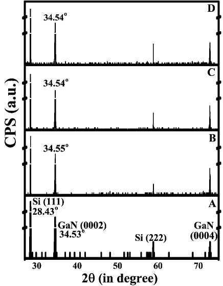
To study the structural properties of Mg doped GaN NRs, we carried out HR-XRD measurements of samples (see Fig 3). From the symmetric 2 scan, we find GaN (0002) reflex, along with Si (111), (222) and GaN (0004) reflexes are present (see Fig.3). Figure 3 suggests all the GaN NRs samples (undoped and Mg-doped) possess single crystallinity, wurtzite structure with a preferential growth direction along the c-axis (0001) with the epitaxial relation of [111]Si [0002]GaN. The intense GaN (0002) reflexes at 34.54o, 34.55o, 34.54o, and 34.54o for samples A, B, C and D respectively suggest with Mg incorporation, c lattice parameter of GaN has reduced, contrary to the typical behavior wherein the lattice parameters of GaN increases as ionic radius of Mg is larger than that of GaKirste et al. (2013). However, if defect such as complexes of N-vacancy are formed, the local strain will change Kirste et al. (2013)and results in the reduction of lattice parameters.
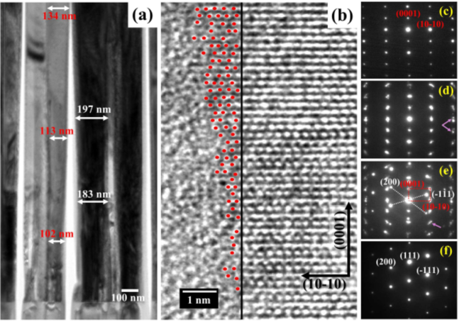
To look at the atomistic origin of coalescence of NRs, we obtained HR-TEM image of samples B and are shown in Fig.4. In Fig.4 (a) the dimensions of two different NRs are shown at different height concluding tapering effect in the NRs sample due to the formation of atomic steps (see red dots in Fig.4(b)). Figure 4 (a) also shows high densities of NRs are formed. Figure 4(c) shows SAED pattern at top part of the NRs where a pattern which is perfectly single crystalline in nature was recorded. However, as we move towards the interface, we started observing other diffraction spots including expected ones (see arrow marked spots in Fig.4 (d) and (e)). As these extra spots are lying on same circle with the other expected spots, we conclude that the extra pattern are due to mosaic nature of NRs. From the SAED pattern of the interface we found that the epitaxial relation between GaN NRs and Silicon substrate are [0002]GaN [111]Si and [110]GaN [01]Si. Absence of any ring pattern in the SAED pattern obtained from interface region further indicates that no amorphous region is formed at the GaN/Si interface.
The observation of high densities of NRs as well as the tapering effect are the main reasons for the coalescence of NRs in this particular case. Along with these factors, the reduction in the values of Hc with an increase in the Mg concentration together suggest that the radial growth rate of sidewall surface of NRs is increasing with an increase in the Mg incorporation. To find the atomistic origin of this enhanced radial growth of NRs we have carried out the first-principles calculations and the next section of the work is dedicated to same.
III.2 Estimation of Diffusion Barrier
It is estimated that for (100) (or ‘m’) plane of GaN, which forms the side wall surfaces of NRs, the diffusion barrior of Ga-adatom shows an anisotropic value. The diffusion barrier along [110] is merely 0.21 eV while along [0001] direction it is 0.93 eV, Lymperakis and Neugebauer (2009) which promotes the radial growth rate of NRs. To study the role of the presence of Mg atoms on the diffusion barrier of adatoms, we estimated the total energy of various configurations where Ga adatoms were kept manually at various position of (100) surface as shown in Fig.5(a) and (b) wherein a 32 in-plane supercell was used. We have taken the similar path in both cases (see Fig.5) for the estimation of diffusion barrier of Ga adatoms along [110] as discussed in work of Lymperakis et al.Lymperakis and Neugebauer (2009) and Jindal et al.Jindal and Shahedipour-Sandvik (2010). Before we discuss about the calculation regarding the estimation of diffusion barrier of Ga adatoms on both the undoped and doped surface, we provide a brief discussion on the atomic structure of both the surfaces. In the relaxed geometry of undoped (100) surface we observed that Ga atoms at top layer of the slab moves inward into the bulk whereas N atoms moves outward into vacuum in comparison to the ideal (100) cleaved surface, which results in the vertical separation of 0.43 Å along and buckling of surface Ga-N bond by 13.45. Because of a such relaxation, we find Ga-N bond reduced to 1.86 Å which is contracted by 6 % w.r.t. the same in bulk. Such a behavior is quite consistent with the other reports in the literatureLandmann et al. (2015); González-Hernández et al. (2014). In case of relaxed surface of Mg doped (100) surface, the atomic relaxation of Ga, Mg and N is bit complex. While Ga atoms moves inward to the bulk, N atoms making bond only with Ga atoms move outward to vacuum. The Mg atoms displaced towards the bulk by 0.10 Å and the N atom that makes bond with Mg atoms moves inward to the bulk by 0.03 Å. The Mg-N bond length at (100) surface is 1.98 Å, while in bulk it is 2.05 Å, which suggests Mg-N bond length shrinks at surface in comparison to bulk by 3.4%.
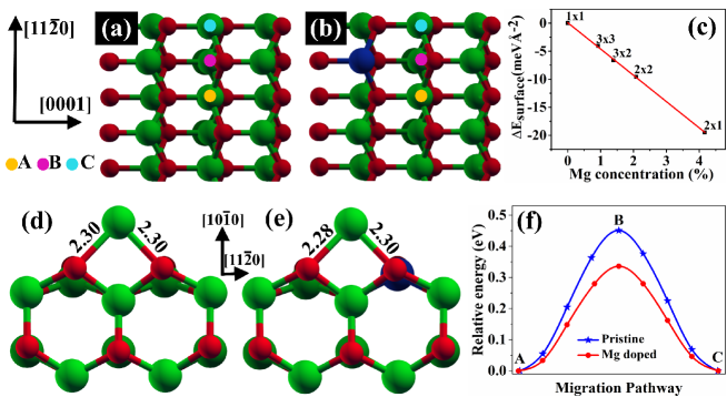
A minimum energy configuration is attained when Ga adatom takes “A” site (see yellow dot in Fig.5 (a)) where it make bond with two surface N atoms with a bond length of 2.30 Å(see Fig.5 (d)). From Mulliken charge analysis we find in this configuration the charge transfer from Ga adatom to the slab is 0.56. Similarly, with Mg doped (100) surface the minimum energy configuration is when Ga adatoms takes “A” site. We find at this configuration the Ga-N bond length are 2.28 Å and 2.30 Å (see Fig.5 (e)) and the charge transfer is 0.59. To estimate the diffusion barrier, we calculated the total energy of various configurations where Ga adatom migrate from one minimum energy configuration (site “A”) to another (site “C”). At undoped surface, we estimated the diffusion barrier as 0.45 eV, while with Mg doped it reduced to 0.33 eV. Such a reduction in the diffusion barrier will increase the diffusion length (Ldiff) of adatoms as Ldiff is proportional to , where represent the average adatom life time. is the diffusion coefficient which is proportional to , where is the diffusion barrier, and are the Boltzmann constant and absolute temperature. By taking the growth temperature as 900 K, we find Ldiff of Ga adatoms on Mg doped surface (with surface Mg concentration as 8.3%) is two times higher than the undoped (100) surface of GaN. Such an increase in the Ldiff is due to the presence of Mg on surface which increases the probability of incorporation of adsorbed Ga adatoms leading to the enhanced radial growth of NRs.
Work of Kaganer et al.Kaganer et al. (2016) suggests that, the nucleation of nanowires are random and homogeneous. After the nucleation, such nanowires attain a self equilibrated diameter beyond which nanowires grow only in the axial direction but not in the radial direction. We propose such a behavior of NRs growth is the reason for the pinning of surface coverage at 802% for higher Mg-doped samples.
IV Summary
In summary, we have synthesized and characterized Mg doped GaN NRs grown on Si (111) surface. We have observed that with an increase in the Mg concentration the surface coverage of the samples increases due to higher growth rate of the sidewall surface of NRs. From TEM analysis we have found that the NRs are tapered as a consequence of the formation of atomic steps on the side surfaces of NRs. From SAED analysis we have found that the NRs nearby interface are more mosaic in nature while mosaicity decreases with the increase in the thickness. From first-principles calculations we have concluded that reduction in the diffusion barrier of Ga ad-atoms due to presence of Mg atoms, on [100] surface, along [110] direction is the primary reason for the higher radial growth rate of NRs.
References
- Tian et al. (2007) B. Tian, X. Zheng, T. J. Kempa, Y. Fang, N. Yu, G. Yu, J. Huang, and C. M. Lieber, Nature 449, 885 (2007).
- Qian et al. (2004) F. Qian, Y. Li, S. Gradecak, D. Wang, C. J. Barrelet, and C. M. Lieber, Nano Letters 4, 1975 (2004).
- Cui et al. (2001) Y. Cui, Q. Wei, H. Park, and C. M. Lieber, Science 293, 1289 (2001).
- Persson et al. (2004) A. I. Persson, M. W. Larsson, S. Stenström, B. J. Ohlsson, L. Samuelson, and L. R. Wallenberg, Nature materials 3, 677 (2004).
- Colombo et al. (2008) C. Colombo, D. Spirkoska, M. Frimmer, G. Abstreiter, and A. F. i Morral, Physical Review B 77, 155326 (2008).
- Glas (2006) F. Glas, Physical Review B 74, 121302 (2006).
- Debnath et al. (2007) R. Debnath, R. Meijers, T. Richter, T. Stoica, R. Calarco, and H. Lüth, Applied Physics Letters 90, 123117 (2007).
- Kim et al. (2005) S.-W. Kim, S. Fujita, and S. Fujita, Applied Physics Letters 86, 153119 (2005).
- Ihn et al. (2006) S.-G. Ihn, J.-I. Song, Y.-H. Kim, and J. Y. Lee, Applied physics letters 89, 053106 (2006).
- Li et al. (2008) L. Li, D. Guimard, M. Rajesh, and Y. Arakawa, Applied Physics Letters 92, 263105 (2008).
- Cerutti et al. (2006) L. Cerutti, J. Ristić, S. Fernández-Garrido, E. Calleja, A. Trampert, K. Ploog, S. Lazic, and J. Calleja, Applied Physics Letters 88, 213114 (2006).
- Wang et al. (2005) Q. Wang, Q. Sun, and P. Jena, Physical Review Letters 95, 167202 (2005).
- Tang et al. (2008) Y. Tang, Z. Chen, H. Song, C. Lee, H. Cong, H. Cheng, W. Zhang, I. Bello, and S. Lee, Nano Letters 8, 4191 (2008).
- Stamplecoskie et al. (2008) K. G. Stamplecoskie, L. Ju, S. S. Farvid, and P. V. Radovanovic, Nano letters 8, 2674 (2008).
- Radovanovic et al. (2007) P. V. Radovanovic, K. G. Stamplecoskie, and B. G. Pautler, Journal of the American Chemical Society 129, 10980 (2007).
- Chen et al. (2009) J. Chen, J. Wang, R. Zhuo, D. Yan, J. Feng, F. Zhang, and P. Yan, Applied Surface Science 255, 3959 (2009).
- Li and Waag (2012) S. Li and A. Waag, Journal of Applied Physics 111, 5 (2012).
- Furtmayr et al. (2008) F. Furtmayr, M. Vielemeyer, M. Stutzmann, J. Arbiol, S. Estradé, F. Peirò, J. R. Morante, and M. Eickhoff, Journal of Applied Physics 104, 034309 (2008).
- Zhang et al. (2009) D. Zhang, C. Xue, H. Zhuang, H. Sun, Y. Cao, Y. Huang, Z. Wang, and Y. Wang, ChemPhysChem 10, 571 (2009).
- Wang et al. (2014) Q. Wang, X. Liu, M. Kibria, S. Zhao, H. Nguyen, K. Li, Z. Mi, T. Gonzalez, and M. Andrews, Nanoscale 6, 9970 (2014).
- Bae et al. (2017) S.-Y. Bae, K. Lekhal, H.-J. Lee, J.-W. Min, D.-S. Lee, Y. Honda, and H. Amano, physica status solidi (b) 254, 1600722 (2017).
- Perdew et al. (1996) J. P. Perdew, K. Burke, and M. Ernzerhof, Physical review letters 77, 3865 (1996).
- Monkhorst and Pack (1976) H. J. Monkhorst and J. D. Pack, Physical Review B 13, 5188 (1976).
- Soler et al. (2002) J. M. Soler, E. Artacho, J. D. Gale, A. García, J. Junquera, P. Ordejón, and D. Sánchez-Portal, Journal of Physics: Condensed Matter 14, 2745 (2002).
- Geelhaar et al. (2011) L. Geelhaar, C. Cheze, B. Jenichen, O. Brandt, C. Pfueller, S. Münch, R. Rothemund, S. Reitzenstein, A. Forchel, T. Kehagias, et al., IEEE Journal of Selected Topics in Quantum Electronics 17, 878 (2011).
- Jenichen et al. (2011) B. Jenichen, O. Brandt, C. Pfueller, P. Dogan, M. Knelangen, and A. Trampert, Nanotechnology 22, 295714 (2011).
- Wierzbicka et al. (2012) A. Wierzbicka, Z. Zytkiewicz, S. Kret, J. Borysiuk, P. Dluzewski, M. Sobanska, K. Klosek, A. Reszka, G. Tchutchulashvili, A. Cabaj, et al., Nanotechnology 24, 035703 (2012).
- Fernández-Garrido et al. (2014) S. Fernández-Garrido, V. Kaganer, C. Hauswald, B. Jenichen, M. Ramsteiner, V. Consonni, L. Geelhaar, and O. Brandt, Nanotechnology 25, 455702 (2014).
- De and Shivaprasad (2016) A. De and S. Shivaprasad, Journal of Physics D: Applied Physics 49, 355304 (2016).
- Kaganer et al. (2016) V. M. Kaganer, S. Fernández-Garrido, P. Dogan, K. K. Sabelfeld, and O. Brandt, Nano Letters 16, 3717 (2016).
- Kirste et al. (2013) R. Kirste, M. P. Hoffmann, J. Tweedie, Z. Bryan, G. Callsen, T. Kure, C. Nenstiel, M. R. Wagner, R. Collazo, A. Hoffmann, et al., Journal of Applied Physics 113, 103504 (2013).
- Lymperakis and Neugebauer (2009) L. Lymperakis and J. Neugebauer, Physical Review B 79, 241308 (2009).
- Jindal and Shahedipour-Sandvik (2010) V. Jindal and F. Shahedipour-Sandvik, Journal of Applied Physics 107, 054907 (2010).
- Landmann et al. (2015) M. Landmann, E. Rauls, W. Schmidt, M. Neumann, E. Speiser, and N. Esser, Physical Review B 91, 035302 (2015).
- González-Hernández et al. (2014) R. González-Hernández, A. González-García, D. Barragán-Yani, and W. López-Pérez, Applied Surface Science 314, 794 (2014).