Ultracompact amplitude modulator by coupling hyperbolic polaritons over a graphene-covered gap
Abstract
The hyperbolic phonon-polaritons within the Reststrahlen band of hBN are of great interest for applications in nanophotonics as they are capable of propagating light signals with low losses over large distances. However, due to the phononic nature of the polaritons in hBN, amplitude modulation of its signal proves to be difficult and has been underexplored. In this paper, we propose theoretically a broadband efficient amplitude modulator for hyperbolic rays in hBN operating in the frequency range between 1450 cm-1 and 1550 cm-1. The modulating region comprises a few tens of nanometers wide gap carved within the hBN slab and covered by a graphene layer, where electrostatically gated graphene serves as a mediator that facilitates the coupling between phonon-polaritons on each side of the gap through plasmonic modes within graphene. We demonstrate that such an ultra compact modulator has insertion losses as low as 3 dB and provides modulation depth varying between 14 and 20 dB within the type-II hyperbolicity region of hBN.
keywords:
Modulator, plasmons, graphene, hBN, hyperbolic raysIR,NMR,UV
Hexagonal boron nitride (hBN) is a natural hyperbolic material that recently attracted a lot of attention due to its prospective applications for mid-infrared nano-photonics 1, 2, 3, 4, 5, 6, 7, 8, 9. The hyperbolic polaritons in hBN within the Reststrahlen band are of phononic nature and thus experience significantly lower losses 10 than their plasmonic counterparts in 2D materials such as graphene, MoS2 and black phosphorus 11. Hence, hBN based waveguides are promising for efficient channeling of signals over large distances in the form of highly-confined sub-diffractional rays 12, 13. However, unlike plasmonic 2D materials, where dispersion of plasmon polaritons is defined by the density of electron gas, the dispersion of phonon-polaritons in hBN, intrinsically originating from oscillations of lattice atoms in a polar crystal, is defined predominantly by the crystal structure. Thus, while the density of electron gas and thus characteristics of polariton modes in plasmonic materials can be actively tuned by applying an electric bias14, 15, 16, 17, 18, achieving a similar degree of control for pure phonon-polariton hBN modes is difficult. As a way to overcome this issue, a huge swath of research has been devoted towards coupling phonon-polaritons in hBN to plasmonic modes in nearby 2D materials, where properties of the hybrid plasmon-phonon modes can be changed by means of electrostatic gating. This has proven to be an effective strategy for active control of plasmon-phonon-polariton dispersion in graphene-hBN heterostructures 4, 19, 6, 20, 21, 22, 7. An alternative approach towards controlling the polariton characteristics in polar dielectrics relies on utilizing phase change materials (PCMs) 23, where changes in the relative permittivity of the PCMs induced by optical pumping can be exploited to alter the polariton dispersion.
Although electrostatic gating of coupled plasmon-phonon modes provides a way of controlling their dispersion characteristics, this does not necessarily lead to an efficient amplitude modulation of a signal carried by the hybrid modes. Meanwhile, signal modulation is one of the most crucial operations in nano-photonics and thus utilizing 2D materials as modulators at telecom wavelengths is of significant interest24. Particularly, electro-optical modulators based on graphene have a high speed of operation, with a modulation speed varying between 1 GHz25, 26, 27 and 35 GHz 28 being reported. Moreover, theoretically imposed limits on the modulation speed exceeds 100 GHz29, 30. The main issue with graphene based optical modulators in near-IR and optical frequency ranges is the weak intrinsic optical absorption of graphene (31, 32) which limits modulation depths for single-layer25, 33 and double-layer26 graphene based modulators to about 0.1 dB m-1. The strength of light-matter interaction and, correspondingly, the modulation depth can be improved by integrating graphene with a dielectric cavity resonator 27, 30, with modulation depths as high as 3.2 dB being demonstrated 27. Unlike the telecom frequency range, in the THz frequency range graphene’s conductivity can be significantly modified by applied electric bias and efficient graphene based modulators have been reported34, 35, 36, 37 with up to 47 modulation being achieved 34 for a modulator operating in the transmission regime. Moreover, the efficient modulation of a quantum cascade laser gain has been reported that utilizes plasmons in graphene incorporated into the laser microcavity for gate tuning38. The mid-IR frequency range provides potential interest for applications in nano-photonics, as this is the range where polar dielectrics, such as hBN, support low-loss highly confined phonon-polaritons. Recently, a nanomechanical graphene/hBN based light modulator operating in the reflection regime (with modulation depth up to 30 ) has been demonstrated 39 in the frequency range from mid-IR up to UV. However, efficient amplitude modulation of the guided phonon-polaritons in hBN has not been explored yet.
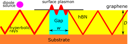
In this paper, we demonstrate that efficient modulation of hyperbolic phonon-polaritons in hBN is indeed possible. We propose an ultra-compact graphene-hBN plasmonic amplitude modulator with a modulation depth of up to 20 dB achieved within a modulating region less than 100 nm long in the frequency range 1450-1550 cm-1, in conjunction with insertion losses of only 3 dB. A sketch of the modulator geometry is presented in Fig. 1a. The core of the modulator is a graphene-covered hBN slab, which, in the frequency range under consideration, allows for signals to propagate in a form of highly directional hyperbolic rays with low losses over large distances. For simplicity, we assume that the signal is injected into the modulator by a line-current source. The modulating region comprises a gap filled with a dielectric and covered by a graphene layer that mediates the coupling between the hyperbolic modes in two neighboring hBN regions. When the graphene is biased to a chemical potential of 0.22 eV, we observe high ( 50) transmission of the hyperbolic mode across the gap. However, the transmission falls more than an order of magnitude when the graphene bias is reduced to 0.12 eV. This can be explained by the strong plasmonic losses within graphene in this range of chemical potentials.
In order to elaborate on the physics underlying the modulator performance, we need to clarify the nature of elementary excitations in the system. In what follows, we restrict our consideration to the frequency range 1400-1570 cm-1, i.e. the window of type-II hyperbolicity in hBN materials19, 4. In this frequency range the optical response of the system is dominated by hyperbolic phonon-polaritons in hBN, plasmons in graphene and hybridized polaritons at the hBN-graphene interface.
The core of the modulator system is an hBN slab of height that allows for signals to propagate over long distances with small losses. The dielectric function of hBN is that of an uniaxial crystal19 with the crystal optical axis orthogonal to the hBN-graphene interface, i.e. , where is the component of permittivity tensor parallel to the optical axis, and
| (1) |
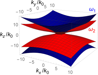
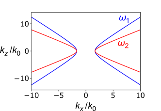
is the component of permittivity tensor orthogonal to the optical axis, where , cm-1, cm-1 and cm-1. In particular, , , and at cm-1, 1500 cm-1, and 1550 cm-1, respectively. As one can see , which indicates that the hBN behaves as hyperbolic material in the above-mentioned frequency range. The term "hyperbolic" stems from the fact that the isofrequency surfaces for an extraordinary wave in lossless materials40 (, which are given by
| (2) |
take the form of a hyperboloid (see Figs. 1b, c). Although hBN is lossy, the losses are extremely small (). Thus, for all practical purposes, hBN behaves as an effectively hyperbolic material. The profile is further reduced to a cone for large values of photon momenta , where is the free-space wavenumber, is the angular frequency, and is the speed of light in vacuum. The direction of energy flow in anisotropic media is defined by the group velocity41, , which points in the direction normal to the isofrequency surface . This means that for sufficiently large values of photon momenta the hyperbolic mode carries energy in a particular direction, constituting an angle () with respect to the optical axis, which is entirely defined by the dielectric function of hBN. These modes are schematically shown as narrow red lines in Fig. 1a. Although high directionality and low losses allow hyperbolic polaritons in hBN to carry energy over long distances, their phononic nature prevents them from being responsive to electric tuning and thus pure hBN hyperbolic modes cannot be used for signal modulation.
The tunability issue can be resolved by coupling hyperbolic phonon-polaritons in hBN with surface plasmons in graphene as shown in Fig. 1a. The wavenumber of a surface plasmon in a graphene monolayer sandwiched between two half-spaces with relative permittivities and is given by the non-linear equation 42
| (3) |
where is the vacuum impedance, , and
| (4) |
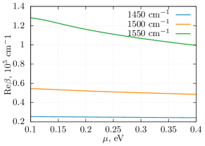
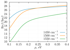
is the optical graphene conductivity 43, 42. Here, denotes the charge of an electron, is the reduced Plank’s constant, is the Boltzmann constant, is the graphene chemical potential, is the Fermi-Dirac distribution, ps and K are electron relaxation time and temperature, respectively. The dispersion and quality factor for surface plasmons in graphene layers in vacuum (i.e. ) are shown in Figs. 1d, e. The graphene plasmons are indeed highly tunable, with graphene losses decreasing significantly as the chemical potential of graphene increases from 0.1 to 0.4 eV and electron mobility decreases from 34000 cm2V/s to 8500 cm2V/s (see SI for relation between mobility and chemical potential in graphene). These mobility values are reasonable for suspended graphene. 44.
The problem, however, arises from the fact that coupled graphene-hBN surface modes are predominantly of phonon character in the frequency range of interest and thus respond significantly more weakly to changes of the graphene chemical potential than graphene plasmons do. The surface modes in air-graphene-hBN-substrate system (see Fig. 1a) are defined by the non-linear equation (see SI for derivation)
| (5) |
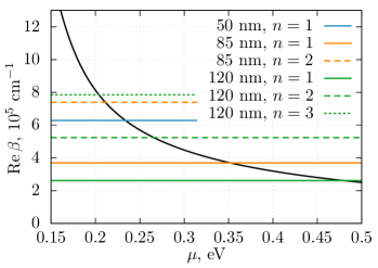
where , , , , , , and is the relative permittivity of the substrate. For a given frequency , the non-linear equation has an infinite number of solutions indicating that such a material slab supports an infinite number of surface modes with increasing wavenumber . The dependence of the wavenumber for the first hybridized graphene-hBN surface mode (i.e. mode with the smallest wavenumber at a given frequency) on the chemical potential of graphene is presented in Figs. 1f, g for the case of a hBN slab of thickness nm and a relative permittivity for the substrate. We are mostly concerned with the first phonon mode as this mode couples most strongly to the dipole excitation and is observed most prominently in scanning near-field optical microscopy and scattering experiments 45, 1, 4. It should be noted, that dispersion of higher order modes is qualitatively similar to that of the first-order mode (see SI for details).
The mode wavenumber increases significantly with frequency ranging from 1450 to 1550 cm-1. This can be explained by the decrease of electrostatic screening with smaller hBN permittivity ( decrease from -10 to -2). However, at any given frequency, dependence of the mode wavenumber (and thus losses) on chemical potential remains weak and thus a bare graphene-hBN system cannot be used to create an efficient optical or polaritonic modulator.
We begin by numerically examining the performance of a modulator based on a graphene-hBN system without dielectric gap; see Fig. 2. All computations are preformed with a time-harmonic Maxwell solver 46 based on the finite element toolkit deal.II 47. A hyperbolic ray, excited at the upper edge of the hBN slab by a current line source, experiences reflection from the bottom of the hBN slab before reaching the graphene-hBN interface on top of the slab where electro-optical modulation occurs. The ray excites hybridized modes at the graphene-hBN surface (Figs. 1f, g) which propagate along the interface until re-radiating their energy back to hBN hyperbolic modes. Losses experienced by the surface mode are responsible for the amplitude modulation of the hyperbolic signal (Fig. 2a). The apparent lateral shift of the "reflected" hyperbolic ray with respect to the incident hyperbolic ray (Fig. 2b) is a manifistation of the Goos-Hanchen effect 48, which we elaborate further below.
We define a transmission value by taking the quotient of the beam intensity around the center of the hBN slab directly before it reaches and directly after it decouples from the graphene-hBN interface (see white dashed lines in Figs. 2c, d). The simulations are done for 1450 - 1550 and 0.1 – 0.5 eV. For values eV the imaginary part of the graphene optical conductivity as given by Eq. (Ultracompact amplitude modulator by coupling hyperbolic polaritons over a graphene-covered gap) becomes negative and graphene cannot support TM plasmon modes anymore. As one can see the transmission increases monotonously from a chemical potential of 0.1 eV to around 0.25 eV. In the case of the graphene-hBN modulator without dielectric gap, the modulation depth achieved varies between 2.62 dB (for 1450 cm-1) and 6.89 dB (for 1550 cm-1) (see Fig. 2a).
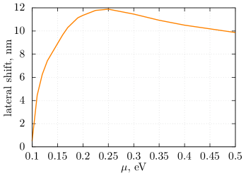
The transmission plateaus for values of chemical potential above 0.25 eV as graphene-hBN plasmon-polariton losses reach a minimal value (see Fig. 1g). It should be pointed out that the transmission of the system in the "on" state (i.e. eV) is only marginally lower than the transmission of hBN without graphene being present, as at high enough chemical potential the losses are mostly defined by phonons in hBN. Despite the relatively low losses in the "on" state, the performance of the modulator (without dielectric gap) suffers from quite high transmission in the "off" state (i.e. for eV). This is due to the fact that surface plasmon-polaritons launched at the interface by hyperbolic rays travel for a relatively short distance before being radiatively decoupled back into bulk hyperbolic modes of hBN (see Figs. 2b, e). Estimations of plasmon travel distance based on the lateral shift experienced by hyperbolic ray hitting graphene-hBN interface are presented in Fig. 2b. We measured this lateral shift by computing the displacement of the hyperbolic beam maximum on the hBN-substrate interface from a reference position obtained with a computation without graphene; see Fig. 2e. As one can see, the value of lateral shift increases from around 2 nm for 0.1 eV to 12 nm at 0.25 eV.
In order to increase the losses in the "off" state, the distance traveled by interface plasmon-polaritons before they radiatively decouple back into hBN has to be increased. Our proposal consists of carving out a length of the hBN slab as illustrated in Fig. 1a. The hyperbolic ray launches surface plasmons on the graphene surface above the gap. These surface plasmons will not be able to decouple into phonon-polaritons of the hBN slab until they reach the other side of the gap. Thus, the losses experienced by plasmons in the "off" state can be significantly increased by increasing the gap width . Unless specified otherwise, we assume that the material inside the gap is air, i.e. the gap permittivity is . The losses in graphene suspended above the gap are presented in Fig. 1e.
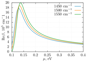
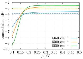
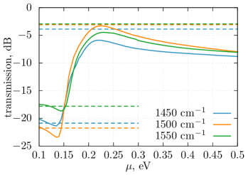
The results of the transmission calculation are shown in Fig. 3a. The transmission increases from a minimum value of around -20 dB at 0.13 eV to -(3–7) dB at around 0.22eV. We obtain an overall modulation depth ranging between 14.2 dB (for 1550 cm-1) to 20.1 dB (for 1500 cm-1). Thus, we can see that the proposed modulator geometry provides efficient modulation in the broad frequency range coinciding with the type-II hyperbolicity region of hBN.
A qualitative understanding of such a behavior can be obtained by studying Fig. 1e and Figs. 3b-d. First of all, we observed that within a range of chemical potential values (around 0.13 eV, see also Fig. 3b), the transmission across the dielectric gap covered by graphene is less than the transmission in case when graphene is absent. Clearly, even if there are no surface plasmons to mediate coupling across the gap between hBN slabs, the edge of the slab where the hyperbolic ray hits the hBN interface serves as a source (though inefficient) of the secondary hyperbolic polaritons in the hBN slab across the gap (transmission of order of -20 dB). However, when the graphene is present, the energy of the hyperbolic ray is mostly transferred to surface modes of the graphene, rather than to the electric field at the edge. As the graphene surface plasmons decay fast (see Fig. 3b) when eV, the amount of energy delivered to the adjacent hBN slab is very small which leads to a strong dip in transmission. As the chemical potential increases plasmon losses in graphene decrease (see Fig. 1e) which leads to an increase in the plasmon propagation distance (see Fig. 3b) and thus to an increased transmission across the gap. The plasmon losses, however, are a monotonously decreasing function whereas the transmission across the gap has pronounced peak around 0.22 eV with transmission values close to those of a system without a gap.
In order to understand this behavior we should take into account that graphene suspended above the dielectric gap behaves effectively as an electrostatically defined ribbon (i.e., a Fabri-Perot resonator), with gap walls serving as ribbon edges (i.e. the ribbon width is equal to that of the gap width). The origin of the pronounced peak in the transmission are geometrical resonances of surface plasmons in the "ribbon", defined by the condition
| (6) |
where defines the resonance order. A strong increase of the electric field for values of the chemical potential corresponding to the geometrical resonance causes a strong increase in transmission, while the case of a weak off-resonant electric field in the cavity leads to a low transmission.
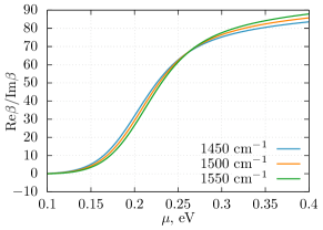
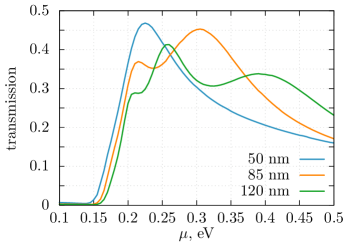
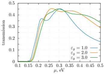
In order to corroborate this conclusion we calculated transmission across gaps of different widths assuming that the gap material is vacuum (see Fig. 4a), and across a gap of fixed width, nm, assuming that the gap is filled with different dielectrics (see Fig. 4b). With the increase of gap width, the resonance peak shift towards higher values of chemical potential. Fig. 4c shows the dispersion relation for a surface plasmon in vacuum superimposed on a set of horizontal lines depicting resonant wavenumbers of cavity modes, obtained using Eq. (6). It follows that the shift is due to a decrease of plasmon wavenumber with the increase in chemical potential. As the increase of the cavity width causes a decrease of the resonance wavenumber, the resonance condition defined by Eq. (6) requires a simultaneous increase in chemical potential. It should be pointed out that the number of resonance peaks in the transmission spectra increases with the increase in cavity width (two resonances for nm and three resonances for nm), as a wider cavity can support high-order resonant modes ( and ).
A fast increase of the plasmon wavenumber at low values of the chemical potential leads to the resonance in transmission spectra around 0.22 eV, the position of which is practically not affected by gap width (compare condition for resonance for nm and resonance for nm in Fig. 4c). The resonance around 0.22 eV is very narrow as plasmonic losses increase drastically below 0.2 eV (see Fig. 1e) and the resonance becomes overdamped. As the chemical potential increases the wavelength of surface plasmons in graphene, , increases (see Fig. 1d) and graphene plasmons become off-resonant when . This causes a strong decrease in the transmission at high values of the chemical potential (see Figs. 4a,b and SI for details).
The analysis of the gap transmission for different dielectric materials filling the gap (Figs. 4b, d) supports the conclusion that the observed transmission peaks are of resonant nature. Again, we can observe a shift of the peaks in the transmission spectra with increasing values of the cavity dielectric function towards higher values of chemical potential (see Fig. 4b). This is due to the increase in plasmon wavenumber with increasing relative permittivity of the substrate (see Fig. 4d) caused by a stronger electrostatic screening.
Concluding, in the paper we proposed the concept of an ultra-compact broadband graphene-hBN modulator operating in the frequency range of type-II hyperbolicity of hBN (1450 cm-1 – 1500 cm-1). The modulating region consists of a few tens of nanometers wide graphene covered gap carved within the hBN slab. By electrostatically gating the graphene, we can turn the coupling between hBN hyperbolic modes on each side of the gap on and off, thus providing efficient modulation of the signal transferred across the gap. Such a modulator has insertion losses as low as 3 dB and a modulation depth as high as 20 dB.
MM, AN, TL, and ML have been partially supported by the Army Research Office (ARO) Multidisciplinary University Research Initiative (MURI) Award No. W911NF-14-1-0247.
Relation between chemical potential and mobility in graphene; derivation of Eq. (5) for surface polaritons in air-graphene-hBN-substrate system; dispersion of second and third-order modes in air-graphene-hBN-substrate system; dependence of transmission across the gap on the chemical potential; dependence of modulation depth and transmission in "off" and "on" state on the gap width.
References
- Dai et al. 2014 Dai, S. et al. Tunable phonon polaritons in atomically thin van der Waals crystals of boron nitride. Science 2014, 343, 1125–1129
- Caldwell et al. 2014 Caldwell, J. D.; Kretinin, A. V.; Chen, Y.; Giannini, V.; Fogler, M. M.; Francescato, Y.; Ellis, C. T.; Tischler, J. G.; Woods, C. R.; Giles, A. J.; Hong, M.; Watanabe, K.; Taniguchi, T.; Maier, S. A.; Novoselov, K. S. Sub-diffractional volume-confined polaritons in the natural hyperbolic material hexagonal boron nitride. Nat. Commun. 2014, 5, 5221
- Caldwell et al. 2015 Caldwell, J. D.; Lindsay, L.; Giannini, V.; Vurgaftman, I.; Reinecke, T. L.; Maier, S. A.; Glembocki, O. J. Low-loss, infrared and terahertz nanophotonics using surface phonon polaritons. Nanophotonics 2015, 4, 44–68
- Dai et al. 2015 Dai, S. et al. Graphene on hexagonal boron nitride as a tunable hyperbolic metamaterial. Nat. Nanotechnol. 2015, 10, 682–686
- Yoxall et al. 2015 Yoxall, E.; Schnell, M.; Nikitin, A. Y.; Txoperena, O.; Woessner, A.; Lundeberg, M. B.; Casanova, F.; Hueso, L. E.; Koppens, F. H.; Hillenbrand, R. Direct observation of ultraslow hyperbolic polariton propagation with negative phase velocity. Nat. Photonics 2015, 9, 674
- Woessner et al. 2015 Woessner, A.; Lundeberg, M.; Gao, Y.; Principi, A.; Alonso-González, P.; Carrega, M.; Watanabe, K.; Taniguchi, T.; Vignale, G.; Polini, M.; Hone, J.; Hillenbrand, R.; Koppens, F. Highly confined low-loss plasmons in graphene-boron nitride heterostructures. Nat. Mater. 2015, 14, 421
- Caldwell et al. 2016 Caldwell, J.; Vurgaftman, I.; Tischler, J.; Glembocki, O.; Owrutsky, J.; Reinecke, T. Atomic-scale photonic hybrids for mid-infrared and terahertz nanophotonics. Nat. Nanotechnol. 2016, 11, 9
- Basov et al. 2016 Basov, D.; Fogler, M.; de Abajo, F. G. Polaritons in van der Waals materials. Science 2016, 354, aag1992
- Low et al. 2017 Low, T.; Chaves, A.; Caldwell, J. D.; Kumar, A.; Fang, N. X.; Avouris, P.; Heinz, T. F.; Guinea, F.; Martin-Moreno, L.; Koppens, F. Polaritons in layered two-dimensional materials. Nat. Mater. 2017, 16, 182–194
- Giles et al. 2017 Giles, A. J.; Dai, S.; Vurgaftman, I.; Hoffman, T.; Liu, S.; Lindsay, L.; Ellis, C. T.; Assefa, N.; Chatzakis, I.; Reinecke, T. L.; Tischler, J. G.; Fogler, M. M.; Edgar, J.; Basov, D.; Caldwell, J. D. Ultra-low-loss Polaritons in Isotopically Pure Materials: A New Approach. arXiv preprint arXiv:1705.05971 2017,
- Avouris et al. 2017 Avouris, P.; Heinz, T. F.; Low, T. 2D Materials; Cambridge University Press, 2017
- Li et al. 2015 Li, P.; Lewin, M.; Kretinin, A.; Caldwell, J.; Novoselov, K.; Taniguchi, T.; Watanabe, K.; Gaussmann, F.; Taubner, T. Hyperbolic phonon-polaritons in boron nitride for near-field optical imaging and focusing. Nat. Commun. 2015, 6, 7507–7507
- Dai et al. 2015 Dai, S.; Ma, Q.; Andersen, T.; Mcleod, A.; Fei, Z.; Liu, M.; Wagner, M.; Watanabe, K.; Taniguchi, T.; Thiemens, M.; Keilmann, F.; Jarillo-Herrero, P.; Fogler, M. M.; Basov, D. Subdiffractional focusing and guiding of polaritonic rays in a natural hyperbolic material. Nat. Commun. 2015, 6, 6963–6963
- Koppens et al. 2011 Koppens, F. H.; Chang, D. E.; García de Abajo, F. J. Graphene plasmonics: a platform for strong light–matter interactions. Nano Lett. 2011, 11, 3370–3377
- Grigorenko et al. 2012 Grigorenko, A.; Polini, M.; Novoselov, K. Graphene plasmonics. Nat. Photonics 2012, 6, 749–758
- Low and Avouris 2014 Low, T.; Avouris, P. Graphene plasmonics for terahertz to mid-infrared applications. ACS Nano 2014, 8, 1086–1101
- Garcia de Abajo 2014 Garcia de Abajo, F. J. Graphene plasmonics: challenges and opportunities. ACS Photonics 2014, 1, 135–152
- Goncalves and Peres 2016 Goncalves, P. A. D.; Peres, N. M. An Introduction to Graphene Plasmonics; World Scientific, 2016
- Kumar et al. 2015 Kumar, A.; Low, T.; Fung, K. H.; Avouris, P.; Fang, N. X. Tunable Light-Matter Interaction and the Role of Hyperbolicity in Graphene-hBN System. Nano Lett. 2015, 15, 3172–3180
- Barcelos et al. 2015 Barcelos, I. D.; Cadore, A. R.; Campos, L. C.; Malachias, A.; Watanabe, K.; Taniguchi, T.; Maia, F. C.; Freitas, R.; Deneke, C. Graphene/h-BN plasmon–phonon coupling and plasmon delocalization observed by infrared nano-spectroscopy. Nanoscale 2015, 7, 11620–11625
- Jia et al. 2015 Jia, Y.; Zhao, H.; Guo, Q.; Wang, X.; Wang, H.; Xia, F. Tunable plasmon–phonon polaritons in layered graphene–hexagonal boron nitride heterostructures. ACS Photonics 2015, 2, 907–912
- Yang et al. 2016 Yang, X.; Zhai, F.; Hu, H.; Hu, D.; Liu, R.; Zhang, S.; Sun, M.; Sun, Z.; Chen, J.; Dai, Q. Far-Field Spectroscopy and Near-Field Optical Imaging of Coupled Plasmon–Phonon Polaritons in 2D van der Waals Heterostructures. Adv. Mater. 2016, 28, 2931–2938
- Li et al. 2016 Li, P.; Yang, X.; Maß, T. W.; Hanss, J.; Lewin, M.; Michel, A.-K. U.; Wuttig, M.; Taubner, T. Reversible optical switching of highly confined phonon-polaritons with an ultrathin phase-change material. Nat. Mater. 2016, 15, 870–875
- Sun et al. 2016 Sun, Z.; Martinez, A.; Wang, F. Optical modulators with 2D layered materials. Nat. Photonics 2016, 10, 227–238
- Liu et al. 2011 Liu, M.; Yin, X.; Ulin-Avila, E.; Geng, B.; Zentgraf, T.; Ju, L.; Wang, F.; Zhang, X. A graphene-based broadband optical modulator. Nature 2011, 474, 64
- Liu et al. 2012 Liu, M.; Yin, X.; Zhang, X. Double-layer graphene optical modulator. Nano Lett. 2012, 12, 1482–1485
- Gao et al. 2015 Gao, Y.; Shiue, R.-J.; Gan, X.; Li, L.; Peng, C.; Meric, I.; Wang, L.; Szep, A.; Walker Jr, D.; Hone, J.; Englund, D. High-speed electro-optic modulator integrated with graphene-boron nitride heterostructure and photonic crystal nanocavity. Nano Lett. 2015, 15, 2001–2005
- Dalir et al. 2016 Dalir, H.; Xia, Y.; Wang, Y.; Zhang, X. Athermal broadband graphene optical modulator with 35 GHz speed. ACS Photonics 2016, 3, 1564–1568
- Gosciniak and Tan 2012 Gosciniak, J.; Tan, D. Theoretical investigation of graphene-based photonic modulators. Sci. Rep. 2012, 3, 1897–1897
- Phare et al. 2015 Phare, C. T.; Lee, Y.-H. D.; Cardenas, J.; Lipson, M. Graphene electro-optic modulator with 30 GHz bandwidth. Nat. Photonics 2015, 9, 511–514
- Mak et al. 2008 Mak, K. F.; Sfeir, M. Y.; Wu, Y.; Lui, C. H.; Misewich, J. A.; Heinz, T. F. Measurement of the optical conductivity of graphene. Phys. Rev. Lett. 2008, 101, 196405
- Nair et al. 2008 Nair, R. R.; Blake, P.; Grigorenko, A. N.; Novoselov, K. S.; Booth, T. J.; Stauber, T.; Peres, N. M.; Geim, A. K. Fine structure constant defines visual transparency of graphene. Science 2008, 320, 1308–1308
- Hu et al. 2016 Hu, Y.; Pantouvaki, M.; Campenhout, J.; Brems, S.; Asselberghs, I.; Huyghebaert, C.; Absil, P.; Thourhout, D. Broadband 10 Gb/s operation of graphene electro-absorption modulator on silicon. Laser Photonics Rev. 2016, 10, 307–316
- Lee et al. 2012 Lee, S.; Choi, M.; Kim, T.; Lee, S.; Liu, M.; Yin, X.; Choi, H.; Lee, S.; Choi, C.; Choi, S.; Zhang, X.; Min, B. Switching terahertz waves with gate-controlled active graphene metamaterials. Nat. Mater. 2012, 11, 936–941
- Sensale-Rodriguez et al. 2012 Sensale-Rodriguez, B.; Yan, R.; Kelly, M. M.; Fang, T.; Tahy, K.; Hwang, W. S.; Jena, D.; Liu, L.; Xing, H. G. Broadband graphene terahertz modulators enabled by intraband transitions. Nat. Commun. 2012, 3, 780
- Sensale-Rodriguez et al. 2012 Sensale-Rodriguez, B.; Yan, R.; Rafique, S.; Zhu, M.; Li, W.; Liang, X.; Gundlach, D.; Protasenko, V.; Kelly, M. M.; Jena, D.; Liu, L.; Xing, H. G. Extraordinary control of terahertz beam reflectance in graphene electro-absorption modulators. Nano Lett. 2012, 12, 4518–4522
- Liang et al. 2015 Liang, G.; Hu, X.; Yu, X.; Shen, Y.; Li, L. H.; Davies, A. G.; Linfield, E. H.; Liang, H. K.; Zhang, Y.; Yu, S. F.; Wang, Q. J. Integrated terahertz graphene modulator with 100% modulation depth. ACS Photonics 2015, 2, 1559–1566
- Chakraborty et al. 2016 Chakraborty, S.; Marshall, O.; Folland, T.; Kim, Y.-J.; Grigorenko, A.; Novoselov, K. Gain modulation by graphene plasmons in aperiodic lattice lasers. Science 2016, 351, 246–248
- Thomas et al. 2016 Thomas, P.; Marshall, O.; Rodriguez, F.; Auton, G.; Kravets, V.; Kundys, D.; Su, Y.; Grigorenko, A. Nanomechanical electro-optical modulator based on atomic heterostructures. Nat. Commun. 2016, 7, 13590
- Poddubny et al. 2013 Poddubny, A.; Iorsh, I.; Belov, P.; Kivshar, Y. Hyperbolic metamaterials. Nat. Photonics 2013, 7, 948–957
- Kong 1986 Kong, J. Electromagnetic wave theory; Wiley-Interscience: New York, 1986
- Hanson 2008 Hanson, G. W. Dyadic Green’s functions and guided surface waves for a surface conductivity model of graphene. J. Appl. Phys. 2008, 103, 064302
- Falkovsky, L. A. and Varlamov, A. A. 2007 Falkovsky, L. A.,; Varlamov, A. A., Space-time dispersion of graphene conductivity. Eur. Phys. J. B 2007, 56, 281–284
- Bolotin et al. 2008 Bolotin, K. I.; Sikes, K.; Jiang, Z.; Klima, M.; Fudenberg, G.; Hone, J.; Kim, P.; Stormer, H. Ultrahigh electron mobility in suspended graphene. Solid State Commun. 2008, 146, 351–355
- Caldwell et al. 2013 Caldwell, J. D.; Glembocki, O. J.; Francescato, Y.; Sharac, N.; Giannini, V.; Bezares, F. J.; Long, J. P.; Owrutsky, J. C.; Vurgaftman, I.; Tischler, J. G.; Wheeler, V. D.; Bassim, N. D.; Shirey, L. M.; Kasica, R.; Maier, S. A. Low-loss, extreme subdiffraction photon confinement via silicon carbide localized surface phonon polariton resonators. Nano Lett. 2013, 13, 3690–3697
- Maier et al. 2017 Maier, M.; Margetis, D.; Luskin, M. Dipole excitation of surface plasmon on a conducting sheet: Finite element approximation and validation. J. Comput. Phys. 2017, 339, 126–145
- Arndt et al. 2017 Arndt, D.; Bangerth, W.; Davydov, D.; Heister, T.; Heltai, L.; Kronbichler, M.; Maier, M.; Turcksin, B.; Wells, D. The deal.II Library, Version 8.5. J. Numer. Math. 2017, in press
- Wu et al. 2015 Wu, J.-S.; Basov, D. N.; Fogler, M. M. Topological insulators are tunable waveguides for hyperbolic polaritons. Phys. Rev. B 2015, 92, 205430