Many-body theory for proton-induced point-defect effects on losses of electron energy and photons in quantum wells
Abstract
The effects of point defects on the loss of either energies of ballistic electron beams or incident photons are studied by using a many-body theory in a multi-quantum-well system. This includes the defect-induced vertex correction to a bare polarization function of electrons within the ladder approximation as well as the intralayer and interlayer screening of defect-electron interactions are also taken into account in the random-phase approximation. The numerical results of defect effects on both energy-loss and optical-absorption spectra are presented and analyzed for various defect densities, number of quantum wells, and wave vectors. The diffusion-reaction equation is employed for calculating distributions of point defects in a layered structure. For completeness, the production rate for Frenkel-pair defects and their initial concentration are obtained based on atomic-level molecular-dynamics simulations. By combining defect-effect, diffusion-reaction and molecular-dynamics models proposed in this paper with a space-weather forecast model for the first time, it will be possible to enable specific designing for electronic and optoelectronic quantum devices that will be operated in space with radiation-hardening protection, and therefore, will effectively extend the lifetime of these satellite onboard electronic and optoelectronic devices.
I Introduction
Point defects (vacancies and interstitials) are produced by displacements of atoms from their thermal-equilibrium lattice sites, book-gary ; book-sigmund where the lattice-atom displacements are mainly caused by a proton-irradiation induced primary knock-on atom (PKA) on a time scale shorter than ps for building up point defects without thermal reactions. These initial displacements are followed immediately by defect mutual recombinations or reactions with sinks (clustering or dissolution of clusters for point-defect stabilizations) add2 ; gao6 on a time scale shorter than ns, then possibly by thermally-activated defect migrations gao5 up to a time scale much longer than ns (steady-state distributions). Such atom displacements depend not only on the energy-dependent flux of protons but also on the differential energy transfer cross sections (probabilities) for collision between atoms, interatomic Coulomb interactions and even kinetic-energy loss to core-level electrons of an atom (ionizations). The sample temperature at which the irradiation has been done also significantly affects the diffusion of defects, their stability as clusters and the formation of Frenkel pairs. gao7 One of the effective calculation methods for studying the non-thermal spatial-temporal distributions of proton-irradiation-induced point defects is the molecular-dynamics (MD) model gao2 . However, the system size increases quadratically with the initial kinetic energy of protons and the time scale can easily run up to several hundred picoseconds. In this case, the defect reaction process driven by thermal migration cannot be included in the MD model due to its much longer time scale. Practically, if the system time evolution goes above ps, either the kinetic lattice Monte-Carlo gao1 or the diffusion-reaction equation ryazanov ; stoller method should be used instead.
In the presence of defects, dangling bonds attached to these point defects can capture Bloch electrons through multi-phonon emission to form localized charged centers. The randomly-distributed charge centers will further affect electron responses to either an external ballistic electron beam book or incident photons add-1 . Physically, the defect modifications to the electron response function can be addressed by a vertex correction add-1 to a bare electron polarization function in the ladder approximation stern (LA). In addition, both the intralayer and interlayer screening corrections in a multi-quantum-well system can be included by using the random-phase approximation stern ; add-3 (RPA). The many-body theory presented here is crucial for understanding the full mechanism for characterizing defects, hallen defect effects, doan as well as for developing effective mitigation in early design stages of electronic devices. Equipped with this multi-timescale microscopic theory, ajss the experimental characterization of post-irradiated test devices hubbs is able to provide useful information on the device architecture’s susceptibility to space radiation effects simoen . Furthermore, our physics model should also allow for accurate prediction of device-performance degradation by using the space weather forecast swf ; cooke for a particular orbit. With this paper, we expect to bridge the gap between researchers studying radiation-induced damage in materials book-gary ; book-sigmund ; add-4 ; add-5 and others characterizing irradiation-induced performance degradation in devices. vince ; chris
The rest of the paper is organized as follows. In Sec. II, we present our theoretical model and numerical results to highlight the defect effects on losses of electron energy and photons in multi-quantum-well systems, where defect potentials and vertex corrections, defect effects on partial and total polarization functions, electron-energy loss functions and intrasubband and intersubband absorption spectra have been demonstrated and analyzed. In Sec. III, ultrafast dynamics related to defect production, as well as the follow-up defect diffusion and reaction, will be studied and a steady-state one-dimensional distribution function of point defects will be calculated to provide a direct input for modeling defect effects discussed in Sec. II. Finally, a summary and some remarks are presented in Sec. IV.
II Effects of point defects
In Sect. II, we first look into effects of point defects on the electron polarization function in a single wide quantum well. After generalizing the system to multiple quantum wells, we further study the kinetic-energy loss of a parallel (or perpendicular) electron beam. For a comparison, we also calculate the loss of incident photons with a field polarization parallel (or perpendicular) to the quantum-well planes, corresponding to intrasubband add-13 (or intersubband add-14 ) optical transitions of electrons, respectively.
II.1 Effects on Electron Polarization Function
Since the wave functions of individual point defects are spatially localized, we expect that the interaction between electrons and charged point defects can only affect the screening to the intralayer Coulomb interaction. Therefore, we start with a study of defect effects in a single quantum well. The exchange-interaction-induced vertex correction to a bare polarization function of electrons in a quantum well has been addressed before add-1 within the ladder approximation.
For an -doped quantum well, the total electron polarization function add-11 can be written as a sum of partial polarization functions, i.e., , where is an electron wavenumber, is an angular frequency of an electrical (or optical) perturbation, and label different energy subbands. Here, each partial polarization function can be calculated through an inverse dielectric function , according to book
| (1) |
where the second term is a defect correction, and the bare polarization function takes the form
| (2) |
is the angle between wave vectors and , is the level broadening, are subband energies, , is the effective mass, is the well width, is the Fermi function, and are the chemical potential and temperature of electrons, respectively.
In addition, the inverse dielectric function in Eq. (1) satisfies
| (3) |
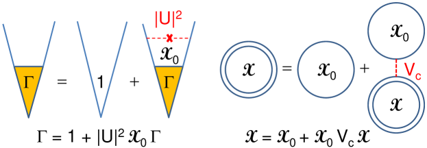
where is the dielectric function and can be calculated within the RPA add-3 as (right panel of Fig. 1)
| (4) |
and the second term corresponds to the defect correction. In Eq. (4), are the intralayer Coulomb matrix elements, given by add-12
| (5) |
where is the host-material dielectric constant, is the wave function of the th subband, and
| (6) |
which plays the role of the inverse of a static screening length. add-12
For the defect-vertex correction add-1 introduced in Eqs. (1) and (4), we find the following self-consistent equation within the LA (left panel of Fig. 1)
| (7) |
where , , and the defect interaction with electrons is calculated as
| (8) |
the sign () corresponds to the case with or ( and ), is the system size, is the trapped charge number of a point defect, , is the correlation length for randomly-distributed point defects, and stands for the one-dimensional distribution function of point defects to be determined later in Sec. III.1. Here, if .
The lowest-order approximate result of Eq. (7) can be obtained simply by replacing with on the right-hand side of this equation. Therefore, the correction to becomes proportional to the total number of point defects or integral of with respect to . In general, the solution of Eq. (7) includes all the higher orders of by going beyond the second-order Born approximation huang .
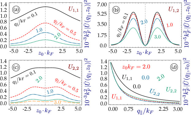
The results calculated from Eq. (8) for are shown in Fig. 2, where the features in with for intrasubband interactions in Figs. 2() and 2() result from the symmetry and anti-symmetry properties of the first two electron wave functions in a quantum well. On the other hand, in Fig. 2() for intersubband interactions displays the overlap of these two electron wave functions with opposite symmetries, leading to two peaks and one node around . From Figs. 2() and 2() we further find that both the peak strength and peak width decrease with increasing , and the reduction of peak strength with can be seen more clearly from Fig. 2(). In addition, a finite value of at leads to a negligible , and furthermore, the widths of the dual peaks in Fig. 2() spread out significantly with .
Based on the calculated in Fig. 2, Eq. (7) can be applied to compute the dynamical defect-vertex correction with respect to unity in the ladder approximation. In order to simulate the physical distribution of defects shown in Fig. 8, we assume a regional form, i.e., , where is a unit-step function and is a scaling number. Similar dependences on both and are seen in Figs. 3() and 3(), respectively, where a very strong intrasubband-scattering resonance associated with a sign switching in ( for ) occurs only within the small-value - region due to the presence of the interaction term in Eq. (7). In this case, the intrasubband-scattering resonance is determined by the peak of
| (9) |
The strength of this intrasubband-scattering resonance decreases rapidly with increasing due to reduced from the suppressed long-range intrasubband scattering as displayed in Fig. 2(). For intersubband excitation with and , on the other hand, the two terms with and are coupled to each other as can be verified by Eq. (7). As a result, the broad intersubband-scattering resonance shows up in Figs. 3() and 3() along with a sign switching in and a peak in . Furthermore, it is very important to notice that the broad intersubband-scattering resonance in Figs. 3() and 3(), due to elastic coupling between and electron states in two subbands, will be different from the sharp intersubabnd-plasmon resonance determined by in Eq. (2).
The calculated in Fig. 3 has been substituted into Eq. (4) to find the intralayer dielectric function modified by defects in the RPA. By using Eq. (3) with this modified dielectric function, the resulting inverse dielectric function has further been input into Eq. (1) to compute related changes in the screened partial polarization functions of a single quantum well. For intrasubband excitations in Figs. 4(), 4() and 4(), the defect-induced change displays a peak shift (sign switching) to a lower and lower value of with increasing . However, reduces significantly for a larger value due to weakened scattering interaction as shown in Fig. 2(). It is also interesting to notice that the depolarization shift of a plasmon peak ( vs. ) in the three insets of (), () and () (with ) also increases with , but it will not show up in for defect effects. This pure plasmon depolarization shift to a higher value is rooted in a many-body screening effect and is slightly reduced by defect scatterings. Similar features in can also be found from Figs. 4() and 4() for intersubband losses, but their magnitudes become much smaller due to very weak intersubband scattering processes. In addition to the shift of this broad intrasubband-plasmon peak by defects, we also expect defect effects on a sharper intersubband-plasmon-loss peak (around ) for a smaller value, as presented in the inset of Fig. 4(), where nearly no shift of the intensive intersubband-plasmon peak is found.
II.2 Effects on Energy Loss of Electron Beams
In Sec II.1, we discussed effects of defects on the intralayer partial polarization function . Here, we extend our study to the kinetic-energy loss of a ballistic electron beam by further taking into account the defect effects on the interlayer total polarization function. A full review on the excitation of collective modes, such as plasmons, in bulk materials, planar surfaces, and nanoparticles was reported, gumbs-1 and the light emission induced by the electrons was proven to be an excellent probe of plasmons, combining subnanometer resolution in the position of the electron beam with nanometer resolution in the emitted wavelength.
Let us assume that a semi-infinite semiconductor occupies the half-space and consider a classical (heavy and slow) point charge moving along a prescribed path in the air space () outside the semiconductor region. In such a case, we find that the external potential associated with this moving charged particle in the quasi-static limit satisfies the instantaneous Poisson’s equation, EELS ; gumbs i.e.
| (10) |
where is the trajectory of the charged particle, and is a position vector. The solution of Eq. (10) inside the region of is found to be
| (11) |
where the Fourier-transformed external potential is calculated as
| (12) |
and its structure factor is
| (13) |
From a physics perspective, the existence of inside the semiconductor will induce a potential outside the semiconductor (i.e., ) due to the charge-density fluctuation, yielding
| (14) |
where is the so-called surface-response function book determined later by matching the boundary condition. Within the semiconductor region (), we write down similar expressions for the external and induced potentials, given by
| (15) |
| (16) |
where is the bare external potential in the electrostatic limit () for a slab of semiconductor material of thickness , , and is the surface-response function for a dielectric slab without doping electrons. book Since the total potential inside the semiconductor () equals the screened external potential, we get in Eq. (16) from nrc
| (17) |
In Eq. (17), the inverse dielectric function can be found from
| (18) |
where the interlayer Coulomb coupling , including the image potentials, is calculated as book
| (19) |
and , .
For a multi-quantum-well system, the density-density-response function in Eq. (18) takes the form EELS
| (20) |
where is the well separation, , and the screened polarization function within the RPA can be obtained from the following self-consistent equations EELS
| (21) |
Here, the summation over excludes the intralayer term with , the integers labels different wells, and is the total polarization function for the th quantum well as discussed in Sec. II.1.
| (22) |
By matching the boundary condition for the total potential, i.e., at the surface , we are able to find the surface response function introduced in Eq. (14) from
| (23) |
where EELS
| (24) |
and the external electrostatic potential in Eqs. (17) and (23) inside a slab of semiconductor () is found to be EELS
| (25) |
The absorbed kinetic energy of an electron beam can be calculated by integrating the Poynting vector over the surface and over time in the air region, which leads to nrc
| (26) |
where is the total potential outside the semiconductor region (), calculated by combining Eqs. (11) and (14) and given by
| (27) |
Substituting this result into Eq. (26), we find
| (28) |
where is the so-called loss function. book
Specifically, for a charged particle moving parallel to the surface, we have and obtain
| (29) |
which leads to the following power absorption for the parallel electron beam
| (30) |
More interesting, if a charged particle moves away from the surface perpendicularly, we can write with an impact parameter () and for the damped particle, and obtain
| (31) |
which yields the energy absorption for the perpendicular electron beam
| (32) |
In this case, the integral over with respect to the loss function includes the damping contributions from both the particle-hole and collective excitation modes of electrons. add-15
Multiple plasmon excitations in graphene materials by a single electron was predicted to give rise to a unique platform for exploring the bosonic quantum nature of these collective modes. gumbs-2 Such a technique not only opens a viable path toward multiple excitation of a single plasmon mode by a single electron, but also reveals electron probes as ideal tools for producing, detecting, and manipulating plasmons in graphene nanostructures.
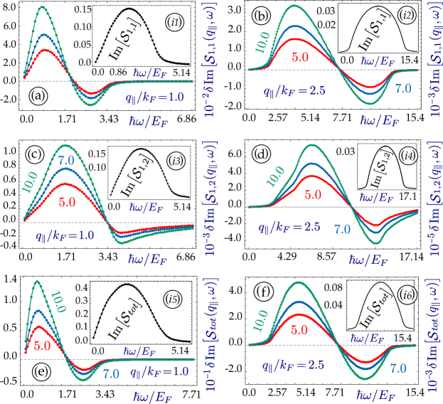
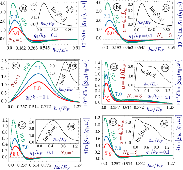
For a single quantum well, the surface response function can be obtained by setting in Eq. (23), and the total loss function is just . Here, the defect induced change directly relates to the imaginary part of the screened partial polarization function presented in Fig. 4. For , we find from Figs. 5(), 5() and 5() that is dominated by for a stronger intrasubband scattering process, which increases with the defect-density scaling number . The sign switching reflects the shift of a loss peak [see insets of Figs. 5(), 5() and 5()] to a lower value of . As is increased to in Figs. 5(), 5() and 5(), the resonant peak of moves to a higher value [see insets () and ()]. However, the similar defect-related features as in Figs. 5(), 5() and 5() are greatly weakened due to a dramatic reduction of scattering interactions as shown in Fig. 2().
For a multi-quantum well system, the interlayer Coulomb coupling in Eq. (21) will modify the intralayer total polarization function , as well as the surface response function in Eq. (23). From the comparison of single- and multi-quantum well systems in Fig. 6, we find the intersubband-plasmon loss is strongly coupled to the intrasubband-plasmon loss by interlayer Coulomb coupling, as shown in the insets of () and (). Here, the weaker peak in the inset () is greatly enhanced by its sitting on the shoulder of a much stronger peak in the inset (), giving rise to a profile for the total peak in the inset (). As , the defect-induced peak shift in to lower can be seen from Fig. 6() but not for in Fig. 6() except for a significant enhancement of the shoulder peak with increasing by interlayer Coulomb coupling. Moreover, by comparing Figs. 6() with 6(), we find both and are dominated by the intralayer Coulomb coupling given by Eq. (5).
II.3 Effects on Loss of Photons
In Sec. II.2, the defect effects on the energy loss of electron beams in a multi-quantum-well system was discussed. As a comparison, the defect effects on the loss of photons (or photon absorption) in the same system will be investigated here. In this case, both the absorption coefficients for intrasubband and intersubband optical transitions of electrons can be calculated from talwar
| (33) |
where is the incident-photon energy, and the dynamical refractive-index function is
| (34) |
For intrasubband transitions with an optical probe field polarized parallel to the quantum-well planes, in Eqs. (33) and (34) is the Lorentz ratio calculated as add-1
| (35) |
where is the radius of a normally-incident Gaussian light beam, is the total number of quantum wells in the system, and the optical-response function add-16 for the th well is found to be
| (36) |
By including the couping due to interlayer Coulomb interactions, the partial polarization function introduced in Eq. (36) with needs to be computed from the following self-consistent equations EELS (taking and afterwards), i.e.,
| (37) |
where , and the interlayer Coulomb matrix elements are still found from Eq. (19). By further taking into account the coupling between different subbands in each quantum well, the screened partial polarization function in Eq. (37) must be calculated from Eq. (1) after finding the inverse dielectric function from Eqs. (3) and (4).
On the other hand, for a spatially-uniform optical probe field polarized perpendicular to the quantum-well planes, the Lorentz ratio in Eqs. (33) and (34) for intersubband transitions becomes add-1
| (38) |
where we have assumed , and is the Fermi wavenumber of electrons in quantum wells. In this case, the optical-response function for the th well in Eq. (38) takes the form add-16
| (39) |
Moreover, the influence of interlayer Coulomb coupling on the intersubband partial polarization function should still be determined from Eq. (37) (setting afterwards).
A periodic stack of graphene layers is expected to have the properties of a one-dimensional photonic crystal with stop bands at certain frequencies. As an incident electromagnetic wave is reflected from these stacked graphene layers, the tuning of the graphene Fermi energy or conductivity renders the possibility of controlling these stop bands, leading to a tunable spectral-selective mirror. gumbs-3 In addition, a transfer-matrix method was applied to explore optical reflection, transmission and absorption in single-, double- and multi-layer graphene structures. gumbs-4 Both the total internal reflection in single-layer graphene, as well as thin-film interference effects in double-layer graphene, are shown for increasing light absorption.
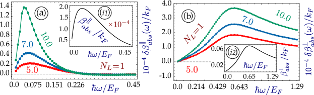
For intrasubband electron transitions induced by an optical field with a polarization parallel to the quantum-well plane, we present in Fig. 7() the defect modification to the absorption coefficient calculated from Eqs. (33) and (35). Here, the low-energy photon absorption peak in the inset () is attributed to the excitation of intrasubband plasmons, and this peak is shifted to an even lower value with increasing . On the other hand, for the intersubband transition of electrons under an optical field polarized perpendicular to the quantum-well plane, we display in Fig. 7() the defect changes in absorption coefficient calculated from Eqs. (33) and (38). In this case, however, a high-energy and broad photon absorption peak in the inset () results from intrasubband-plasmon excitations, and no shift associated with this peak with is found.
III Ultrafast Point-Defect Dynamics
In Sec. II, we only discuss the effects of point defects on losses of electron energy and photons in a multi-quantum-well system. In Sec. III, we explore ultrafast dynamics for the production of Frenkel-pair defects and their follow-up reactions and diffusions in the same system. In this way, the spatial dependence of the one-dimensional distribution function introduced in Eq. (7) for the defect-electron interaction can be extracted. It is known that the Frenkel-pair production will be followed subsequently by diffusion and reactions to reach defect stabilization through diffusion-induced recombination and reactions with residual defects in the system. Here, the diffusion of point defects is driven by forces other than the concentration gradient of defects, e.g., compressive stress near sinks. The reactions, on the other hand, are enabled by the presence of growth-induced dislocation loops at the two interfaces of a quantum well.
III.1 Defect Diffusion-Reaction Equations
Let us start by considering an layered material structure in the direction. Each material layer is characterized by the (bulk) irradiation parameters , , and with layer labels for production and recombination rates, diffusion coefficient and bulk-sink annihilation, respectively. In modeling a mesoscopic-scale sample, the interface-sink strengths with also need to be taken into account.
For a reaction-rate control system, we can write down the diffusion-reaction equations book-gary for the concentrations of point vacancies and interstitial atoms as
| (40) | |||||
| (41) | |||||
where the small thermal-equilibrium concentration of point vacancies has been neglected at low temperatures, the terms on the right-hand side of the equations correspond to diffusion sources and reactions, integer is the layer index, integer indicates the number of interstitials enclosed within a planar dislocation loop bullough , and represent the left and right interface positions of the th layer, and are the concentrations of point vacancies and interstitials, and are the diffusion coefficients, and is the production rate for Frenkel pairs. Here, can be obtained by multiplying the sample cross-sectional area with and . In addition, in Eqs. (40) and (41), we used the facts that in a reaction-rate control system for the vacancy-interstitial recombination rate, is the rate for the interaction between defects and interface dislocation loops, and for the dislocation loop-sink strength, where is the bias factor for recombinations book-gary , is the atomic volume, is the lattice constant, and is the initial number of Frenkel pairs. Furthermore, and are the bias factors for the reactions and the capture radii of vacancy-dislocation loop () and interstitial-dislocation loop (), are the bias factors for vacancies and interstitials, and finally is the growth-strain-induced interface dislocation-loop (enclosing captured interstitial atoms) areal density.
The diffusion coefficients for point vacancies and interstitials can be calculated from book-gary
| (42) |
where are the migration energies for point vacancies and interstitials, is determined by the diffusion mechanism and crystal symmetry, is the Debye frequency and is the sound velocity of the host semiconductor.
The interface dislocation-loop density in Eqs. (40) and (41) can be found from the following reaction equation book-gary (for ), i.e.
| (43) |
where and is the initial density for the smallest interface dislocation loops containing four interstitials, the absorption [] and the emission [] rates are given by book-gary
| (44) |
| (45) |
and is the binding energy for a planar cluster of interstitials.
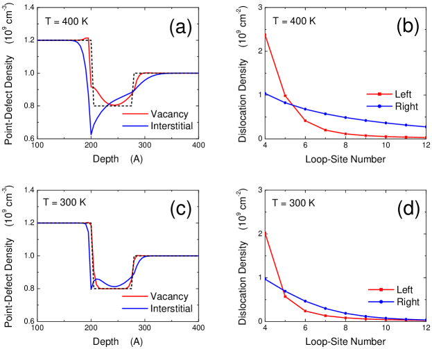
We show in Figs. 8() and 8() the steady-state spatial distributions for concentrations of point vacancies and interstitials in an AlAs/InAs/GaAs single-quantum-well system. We notice from Eqs. (40), (41) and (43) that both and in a steady state eventually become proportional to although is initially proportional to . Here, the comparison of results at K (upper) and K (lower) are presented to demonstrate the diffusion of point vacancies into the well through both interfaces due to thermally-enhanced diffusion coefficients of vacancies. However, the interstitial concentration around the left interface is greatly depleted (deep dip) at K as a result of large absorptions by dislocation loops although they still diffuse into the well through the right interface. In Figs. 8() and 8(), we display results for steady-state distributions of dislocation-loop densities () as functions of loop-site number, corresponding to the left () and right () interfaces at and K. Here, the increases of dislocation-loop densities () at the left interface and the simultaneous swellings of dislocation loops () at the right interface are found due to the enhanced reactions with point interstitials by their increased diffusion coefficients. Moreover, the defect diffusions occur mainly around interfaces between two adjacent layers or across the interfaces, and due to their different diffusion coefficients although these two concentrations are initially identical.
III.2 Defect Production by Proton Radiation
The diffusion-reaction equations presented in Sec. III.1 can be applied to find the spatial dependence of the one-dimensional distribution function of defects. However, the initial conditions of these equations require the production rate and the concentration of proton-produced Frenkel pairs. Therefore, we must study the production dynamics of point defects under proton irradiation with different kinetic energies, which connects the lab-measured defect effects ( number of point defects) to space-measured energy-dependent proton fluxes in a particular earth orbit. For this purpose, an atomic-level molecular-dynamics simulation approach is employed with help from a Tersoff potential fitted by parameters. add10 ; gao-1
For a bulk material, the production rate per unit volume [seccm-3] for the displacement atoms in a crystal lattice can be calculated from book-gary
| (46) |
where [MeV] is the incident proton kinetic energy, [cm-3] is the crystal atom volume density, [cmsec-1] is the incident energy-dependent proton flux, and [cm2] is the energy-dependent displacement cross section.
Physically, the displacement cross section in Eq. (46) describes the probability for the displacement of struck lattice atoms by incident protons, therefore, we can directly write
| (47) |
where [cm] is the differential energy transfer cross section by collision with the lattice, which measures the probability that an incident proton with kinetic energy will transfer a recoil energy [keV] to a struck lattice atom, [no unit] represents the average number of displaced atoms produced by collision with the lattice, and labels the energy threshold, i.e., the energy required to produce a stable Frenkel pair. In addition, is the upper limit for the recoil energy gained by the struck lattice atom, where refers to the mass of lattice atoms and to the mass of incident protons.
The function [unitless] introduced in Eq. (47) is the so-called Lindhard partition function and is written as niel ; niel1 ; niel2
| (48) |
where the Ziegler-Biersack-Littmark (ZBL) reduced-energy is defined as
| (49) |
while the reduced electronic energy-loss factor is
| (50) |
kg is the proton mass, is the ZBL universal screening length, Å is the Bohr radius, is the free-electron mass, and the Lindhard function is calculated as
| (51) |
In the current case, we set (proton), (Ga) or (As) for the nuclear charge number of lattice atoms.
Moreover, the differential energy transfer cross section [cm] can be approximated as niel2
| (52) |
where is the dimensionless collision parameter, is the scaled ZBL reduced energy. The function introduced in Eq. (52) is defined as
| (53) |
where , , , , and are four parameters.
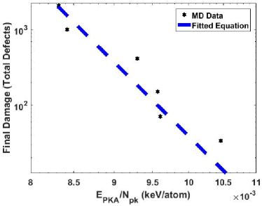
Finally, in Eq. (47) can be computed by using MD simulations. As shown in Fig. 9, the calculated can be fitted reasonably well by a simple power law, i.e., with proper fitting parameters and . Finally, by combining together the results in Eqs. (46)-(52), for a given flux spectrum we get the production rate per unit volume as
| (54) |
which can be evaluated numerically once fitting parameters and are obtained. Here, is related to the more familiar non-ionizing energy loss add-4 by with being a crystal atom weight density. add-4 Furthermore, the concentration for Frenkel-pair defects can be roughly estimated from , where is the effective proton transit time through the sample, and ns, which is proportional to , is the time required to reach a steady state for generation of Frenkel-pair defects after the production has been balanced by the recombination.
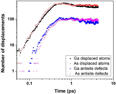
We present in Fig. 10 the numerical results for calculated number of lattice-atom displacements as a function of time after a Ga PKA has been introduced to a GaAs crystal with the recoil energy keV. From Fig. 10, we find that the number of lattice-atom displacements reaches a peak value at about ps. After this peak time, only of the displaced atoms recombine with vacancies, and most anti-site defects are generated during the collisional phase. In addition, a steady state with keV has been reached for ps, where As defects are slightly higher than that of Ga defects due to the smaller formation energy for As defects add-5 .
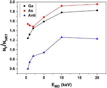
The numerical results for the number of Ga and As displaced atoms and anti-site defects as a function of recoil energy at ps are displayed in Fig. 11, where the NRT result is given by . It is clear from this figure that the number of defects in steady state is found to be much high than that given by the NRT value. Moreover, nonlinear dependence on is limited only for low-energy PKA recoils.
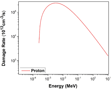
In order to provide initial Frenkel-pair defect concentrations and its production rate, we show in Fig. 12 the numerical result of Eq. (54) for . It is clear from this figure that there exists a peak for as a function of incident proton kinetic energy due to competition between increasing and decreasing at the same time.
IV Summary and Remarks
In conclusion, we have investigated the effects of point defects on the loss of either electron kinetic energy or incident photons in a multi-quantum-well system. The influence of proton-radiation-produced defects is taken into account by applying the vertex correction to a bare polarization function of electrons in quantum wells within the ladder approximation, which goes beyond the usual second-order Born approximation. Both intralayer and interlayer dynamical screenings to the defect-electron interaction have also been considered under the random-phase approximation. Furthermore, the defect effects on the electron-energy loss function, as well as on intrasubband and intersubband optical absorption, have been shown and discussed.
To find the distribution function of point defects in a layered structure for calculations of defect effects, we have applied the diffusion-reaction-equation method, where the reactions of point defects with the growth-induced dislocation loops on interfaces of the multi-layered system have been included, and the increase and decrease of dislocation-loop density and point-defect concentrations were found at the same time due to thermal enhancement of defect diffusion. In addition, the Frenkel-pair defect production rate and the initial concentration of Frenkel pairs were obtained from an atomic-level molecular-dynamics model after fitting the numerical results for Frenkel pairs as a function of energy of a primary knock-on atom.
For the first time, the defect effect, diffusion-reaction and molecular dynamics models presented in this paper can be combined with a space-weather forecast model swf ; cooke which predicts spatial-temporal fluxes and particle velocity distributions. With this combination of theories, the predicted irradiation conditions for particular satellite orbits allow electronic and optoelectronic devices to be specifically designed for operation in space with radiation-hardening considerations ajss (such as self-healing and mitigation). This approach will effectively extend the lifetime of satellite onboard electronic and optoelectronic devices in non-benign orbits and greatly reduce the cost.
Acknowledgements.
This material is based upon work supported by the Air Force Office of Scientific Research (AFOSR). We would also like to thank Dr. Paul D. LeVan and Dr. Sanjay Krishna for helpful discussions.References
- (1) G. S. Was, Fundamentals of Radiation Materials Science: Metals and Alloys (Springer-Verlag, Berlin, Heidelberg, 2007).
- (2) P. Sigmund, Particle Penetration and Radiation Effects (Springer-Verlag, Berlin, Heidelberg, 2006).
- (3) K. Nordlund, J. Peltola, J. Nord, J. Keinonen, and R. S. Averback, J. Appl. Phys. 90, 1710 (2001).
- (4) R. Devanathan, W.J. Weber, and F. Gao, J. Appl. Phys. 90, 2303 (2001).
- (5) M. Posselt, F. Gao, and D. Zwicker, Phys. Rev. B 71, 245202 (2005).
- (6) F. Gao and W.J. Weber, J. Appl. Phys. 94, 4348 (2003).
- (7) F. Gao, H. Xiao, X. Zu, M. Posselt, and W.J. Weber, Phys. Rev. Lett. 103, 027405 (2009).
- (8) Z. Rong, F. Gao, and W.J. Weber, J. Appl. Phys. 102, 103508 (2007).
- (9) L. A. Maksimov and A. I. Ryazanov, Sov. Phys. JETP 52, 1170 (1980).
- (10) S. I. Golubov, A. V. Barashev, and R. E. Stoller, Comprehensive Nuclear Materials, edited by R. Konings, R. Stoller, T. Allen, and S. Yamanaka (Elsevier Ltd., Amsterdam, 2012), ch. 13.
- (11) G. Gumbs and D. H. Huang, Properties of Interacting Low-Dimensional Systems (Wiley-VCH Verlag GmbH & Co. KGaA, Boschstr, Weinheim, 2011).
- (12) D. H. Huang and M. O. Manasreh, Phys. Rev. B 54, 5620 (1996).
- (13) T. Ando, A.B. Fowler and F. Stern, Rev. Mod. Phys. 54, 437 (1982).
- (14) G. Gumbs, D. H. Huang, Y. Yin, H. Qiang, D. Yan, F. H. Pollak, and T. F. Noble, Phys. Rev. B 48, 18328 (1993).
- (15) A. Hallén, D. Fenyö, B. U. R. Sundqvist, R. E. Johnson, and B. G. Sevensson, J. Appl. Phys. 70, 3025 (1991).
- (16) N. V. Doan and G. Martin, Phys. Rev. B 67, 134107 (2003).
- (17) D. H. Huang, F. Gao, D. A. Cardimona, C. P. Morath and V. M. Cowan, Am. J. Space Sci. 3, 3 (2015).
- (18) C. Claeys and E. Simoen, Radiation Effects in Advanced Semiconductor Materials and Devices (Springer, 2002).
- (19) J. E. Hubbs, P. W. Marshall, C. J. Marshall, M. E. Gramer, D. Maestas, J. P. Garcia, G. A. Dole, and A. A. Anderson, IEEE Trans. Nucl. Sci. 54, 2435 (2007).
- (20) M. Moldwin, An Introduction to Space Weather (Cambridge University Press, New York, 2008).
- (21) D. L. Cooke and I. Katz, J. Spacecraft & Rockets, 25, 132 (1988).
- (22) F. Gao, N. J. Chen, E. Hernandez-Rivera, D. H. Huang, and P. D. LeVan, J. Appl. Phys. 121, 095104 (2017).
- (23) N. J. Chen, S. Gray, E. Hernandez-Rivera, D. H. Huang, P. D. LeVan, and F. Gao, J. Materials Research 32, 1555 (2017).
- (24) V. M. Cowan, C. P. Morath, J. E. Hubbs, S. Myers, E. Plis and S. Krishna, Appl. Phys. Lett. 101, 251108 (2012).
- (25) C. P. Morath, V. M. Cowan, L. A. Treider, G. Jenkins and J. E. Hubbs, IEEE Trans. Nucl. Sci. 62, 512 (2015).
- (26) D. H. Huang and S.-X. Zhou, Phys. Rev. B 38, 13061 (1988).
- (27) D. H. Huang and S.-X. Zhou, Phys. Rev. B 38, 13069 (1988).
- (28) D. H. Huang, G. Gumbs and N. J. M. Horing, Phys. Rev. B 49, 11463 (1994).
- (29) D. H. Huang and M. O. Manasreh, Phys. Rev. B 54, 2044 (1996).
- (30) D. H. Huang, P. M. Alsing, T. Apostolova and D. A. Cardimona, Phys. Rev. B 71, 195205 (2005).
- (31) F. J. García de Abajo, Rev. Mod. Phys. 82, 209 (2010).
- (32) G. Gumbs, Phys. Rev. B 39, 5186 (1989).
- (33) G. Gumbs and N.J.M. Horing, Phys. Rev. B 43, 2119 (1991).
- (34) B. N. J. Persson and E. Zaremba, Phys. Rev. B 31, 1863 (1985).
- (35) A. Iurov, G. Gumbs, D. H. Huang and V. Silkin, Phys. Rev. B 93, 035404 (2016).
- (36) F. J. García de Abajo, ACS Nano 7, 11409 (2013).
- (37) G. Gumbs, D. H. Huang, and D. N. Talwar, Phys. Rev. B 53, 15436 (1996).
- (38) D. H. Huang, C. Rhodes, P. M. Alsing, and D. A. Cardimona, J. Appl. Phys. 100, 113711 (2006).
- (39) Yu. V. Bludov, N. M. R. Peres, and M. I. Vasilevskiy, J. Opt. 15, 114004 (2013).
- (40) T. Zhan, X. Shi, Y. Dai, X. Liu, and J. Zi, J. Phys.: Condens. Matt. 25, 215301 (2013).
- (41) R. Bullough, M. R. Hayns, and C. H. Woo, J. Nucl. Mater. 84, 93 (1979).
- (42) J. Tersoff, Phys. Rev. B 37, 6991 (1988).
- (43) F. Gao, and W. J. Weber, Phys. Rev. B 63, 054101 (2000).
- (44) S. R. Messenger, E. A. Burke, M. A. Xapsos, G. P. Summers, R. J. Walters, I. Jun, and T. Jordan, IEEE Trans. Nucl. Sci. 50, 1919 (2003).
- (45) J. F. Ziegler, J. P. Biersack, and U. Littmark, The Stopping and Range of Ions in Solids (vol. I, Pergamon Press, New York, 1985).
- (46) M. Nastasi, J. W. Mayer, and J. K. Hirvonen, Ion-Solid Interactions, Fundamentals and Applications (Cambridge Univ. Press, New York, 2004).