Electrical properties of single crystal Yttrium Iron Garnet ultra-thin films at high temperatures
Abstract
We report a study on the electrical properties of 19 nm thick Yttrium Iron Garnet (YIG) films grown by liquid phase epitaxy. The electrical conductivity and Hall coefficient are measured in the high temperature range [300,400] K using a Van der Pauw four-point probe technique. We find that the electrical resistivity decreases exponentially with increasing temperature following an activated behavior corresponding to a band-gap of eV, indicating that epitaxial YIG ultra-thin films behave as large gap semiconductor, and not as electrical insulator. The resistivity drops to about at K. We also infer the Hall mobility, which is found to be positive (-type) at 5 cm2/(Vsec) and about independent of temperature. We discuss the consequence for non-local transport experiments performed on YIG at room temperature. These electrical properties are responsible for an offset voltage (independent of the in-plane field direction) whose amplitude, odd in current, grows exponentially with current due to Joule heating. These electrical properties also induce a sensitivity to the perpendicular component of the magnetic field through the Hall effect. In our lateral device, a thermoelectric offset voltage is produced by a temperature gradient along the wire direction proportional to the perpendicular component of the magnetic field (Righi-Leduc effects).
The recent discovery that spin orbit effects Valenzuela and Tinkham (2006); Kajiwara et al. (2010); Miron et al. (2011); Rojas-Sánchez et al. (2013) could allow to generate or to detect pure spin currents circulating in an adjacent magnetic layer has triggered a renewed interest for magnon transport in magnetic oxides, and in particular Yttrium Iron garnet, Y3Fe5O12 (YIG) Kajiwara et al. (2010); Wang et al. (2011); Padrón-Hernández et al. (2011); Chumak et al. (2012); Hahn et al. (2013); d’Allivy Kelly et al. (2013); Hamadeh et al. (2014); Collet et al. (2016); Lauer et al. (2016); Du et al. (2017); Wesenberg et al. (2017); Thiery et al. (2017), the material with the lowest known magnetic damping in nature. It confers to YIG the unique ability to propagate the spin information on the largest possible distance. Moreover, as YIG is an electrical insulator, all spurious effects associated with electrical transport properties are absent, which simplifies greatly the interpretation of the measurements.
The latest studies on the magnon transport properties of YIG concentrate on the strong out-of-equilibrium regime where large spin currents are induced in the YIG either by way of spin transfer torque Wesenberg et al. (2017); Thiery et al. (2017) or by temperature gradients Safranski et al. (2017); Lauer et al. (2016). When performed at room temperature, this involves heating the YIG material well above 300 K. One possible concern is the potential increase of its electrical conductivity at high temperature. Indeed, it has been known since the seventies Larsen and Metselaar (1976); Metselaar and Larsen (1978); Lal et al. (1982); Petrov et al. (1986); Sirdeshmukh et al. (1998); Modi and Sharma (2014) that the electrical resistivity of doped YIG could decrease by several orders of magnitude at high temperature due to the presence of impurities. In the case of ultra-thin films defects could come from the growth method or from the 2 interfaces and potentially lead to a spurious charge conduction channel when heated well above 300 K. In order to clarify this point, we propose to investigate the evolution of the electrical properties of single crystal Yttrium Iron Garnet ultra-thin films at high temperatures.
Before describing the experimental procedure, we would like to recall that YIG is a ferrimagnet, which has an uncompensated magnetic moment on the Fe3+ ions, found on octahedral and tetrahedral coordinate sites, both coupled by super-exchange. Studies on Ca and Si doped YIG Larsen and Metselaar (1976) have established that Fe2+ and Fe4+ ions are formed if tetravalent or respectively divalent impurities are added to the YIG, which could then lead to an electrical conduction via the charge transfer mechanism, respectively -type and -type. In that case, the doped YIG behaves as a large gap semiconductor with a charge conductivity following an activation mechanism. At the present stage, different studies disagree about the microscopic mechanism at play for the electronic conduction inside doped YIG, whether it follows a localized hopping model, through a small polaron conduction Sirdeshmukh et al. (1998) or rather a band model, through a large polaron conduction Larsen and Metselaar (1976). It is also known that the value of the magnetic damping coefficient of YIG is very sensitive to the doping level. This is because the charge transfer between the mixed valence iron ions is associated to a potent magnetic relaxation process, known as the valence exchange relaxation Sparks (1969). So far this mechanism activated by impurities, appears in the form of a large enhancement of the magnetic damping, usually around liquid nitrogen temperature, where the fluctuation rate of the charge transfer matches the Larmor frequency. This effect is usually minimized by growing YIG crystals from ultra-pure materials. Quite remarkably YIG can usually be synthesized in large volume in the form of a single crystal with almost no atomic disorder. It has been reported that the resistivity of bulk ultra-pure YIG can be as large as at room temperature Metselaar and Larsen (1978).
But, as explained in the introduction, recent interest on spin transfer effects in YIG have required an effort to develop high quality YIG material in the form of ultra-thin (below 20 nm) films (thickness should be compared here relatively to the YIG unit cell, which is 1.238 nm). This is because spin transfer effect is an interfacial phenomenon and consequently its efficiency increases with decreasing thickness of the magnetic layer. Three growth techniques have so far allowed to produce good quality ultra-thin YIG films: sputtering Fang et al. (2017); Kang et al. (2005); Wang et al. (2013); pulsed laser deposition d’Allivy Kelly et al. (2013); Sun et al. (2012); Onbasli et al. (2014); Hauser et al. (2016); and liquid phase epitaxy (LPE) Thiery et al. (2017); Dubs et al. (2017); Hahn et al. (2013). These films are usually grown on Gadolinium Gallium Garnet, Gd3Ga5O12 (GGG) substrates, which provides the necessary lattice matching to achieve epitaxial growth. For all these three growth processes, the quality of the YIG films deteriorates as the film thickness decreases d’Allivy Kelly et al. (2013); Dubs et al. (2017). This deterioration is an inherent consequence of an increasing surface to volume ratio, which substantially enhances the possibilities for defects and impurities to be introduced into the YIG, through the two surfaces (contamination, intermixion of the species at the surface or unrelaxed strains in the film thickness), which leads to lower spontaneous magnetization and an out-of-plane anisotropy accompanied or not by an increase of the coercive field.
So far, the highest thin film quality (smallest combination of low magnetic damping parameter, low inhomogeneous broadening, and film thickness below 20 nm) have been reported for thin films grown by the LPE technique, an extension of the flux method. Garnets have a non-congruent melting phase and can only be prepared in the form of single crystals once dissolved in a solvent. The solvent used is usually a mixture of different oxides elements, mainly PbO and B2O3, which can eventually enter as impurities in the flux growth. The molten mixture is confined in a platinum crucible (inert with respect to the oxides) placed in an epitaxy furnace above the saturation temperature, defined as the temperature at which the growth rate is zero. Subsequently, the GGG substrate with crystallographic orientation (111) is immersed in the bath. Optimization of the growth process parameters is achieved by studying the dependencies of the depositing conditions on the structural, morphological and magnetic properties. The key to very good growth, is to keep the solution perfectly homogeneous and the growth rate very slow. The main problem is the difficulty of developing a recipe leading to YIG films homogeneous in both thickness and composition. Indeed, for very thin layers, the role of the transition layer is essential (chemical composition) and requires a control of the chemical elements composing it. Indeed, the influence of this transition layer on the different contributions to the line width is important. The YIG films, that we have developed from LPE growth technique, have the following characteristics: perfect epitaxy (difference of matching parameter with the substrate is null); spontaneous magnetization almost equal to that of the bulk ( of our 19 nm YIG films is about 1.7 kG); very low magnetic relaxation (damping coefficient less than or equal than ); no planar anisotropy and very weak coercive field ( Oe); very low roughness (3 Å).
| YIG | (nm) | (G) | (Oe) | |
|---|---|---|---|---|
| 19 | 2.5 |
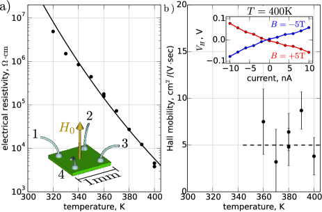
In the following we will concentrate on the electronic properties of LPE grown YIG thin films of thickness nm. The dynamical characteristics of these films are summarized in Table 1. A 11mm2 square slab of YIG is extracted from the batch and connected along the 4 corners using Al wire bonding. To characterize the slab we use the van der Pauw four probes method, which is typically used to measure the sheet resistance of homogeneous semiconductor films. It allows to eliminates measurement errors associated with the exact shape of the sample. The four points are arranged in a clockwise order around the positive field normal shown schematically inside FIG.1a. Because of YIG high impedance, we have used a Keithley 2636B source-measurement unit in order to draw very little current (sub-nA range) inside the film. In our analysis, the GGG substrate will be considered a good insulator (resistivity ) Metselaar and Larsen (1978) and its electrical conductivity will be ignored.
Our measurements are performed at high temperature in the range [300,400] K and for different magnetic fields in the range [0,5] T applied normally to the sample surface. The temperature range explored is still well below the Curie temperature of YIG, which is K. We first extract the sheet resistance , which consists in measuring all possible combinations of the cross-resistance between opposite edges. From the van der Pauw expression, one can extract , whose minimum lays in the couple of G range at the highest temperature. From the sheet resistance, we compute the resistivity . FIG.1 shows the resistivity as a function of temperature. The first remarkable feature is that the resistivity of YIG at 400K drops to about . Plotting the data on a semi-logarithmic scale helps to show that the decay of the resistivity follows an exponential behavior. Fitting a linear slope through the points on the plot, we infer a band-gap energy of about 2 eV, which is about 1 eV lower than the expected band-gap of pure YIG in bulk form.
Next, we characterize the Hall conductance of our sample. For this, we now circulate the electrical current along the diagonals and measure the voltage drop along the opposite contacts . Here is the contact number modulo 4, where the subscript notation is ordered according to the connections to the high/low binding posts of the current source and voltmeter. The insert of FIG.1b shows the voltage drop measured at 400 K in the presence of a normal magnetic field of 5 T. To eliminate the resistivity offset, we have worked out the difference of the voltages for positive and negative magnetic fields. In our measurement geometry, the polarity of the Hall voltage is opposite to the magnetic field direction. It implies that the trajectories of the charge carriers are deflected in the opposite direction to the current in the electromagnet, or in other words that the YIG behaves as a -type conductor. Quantitatively the full variation of the Hall voltage is about 0.12 V at 10 nA when the field is changed by 5 T at 400 K, where the YIG resistivity is cm. This corresponds to a carrier mobility for the holes of about cm2/(Vsec). We have repeated the measurement for other temperatures. The measurement at lower temperature is difficult for 2 reasons. The first one is the limited voltage range of the sourcemeter, which decreases the upper current limit that could be injected in the YIG. Another consequence of the large resistivity, is the associated increase of the time constant for charging effects. This increases substantially the dwell time necessary before taking a measurement. Because of these difficulties, we have limited the measurement range to 40 K below the maximum temperature. It seems that the temperature dependence of the mobility as a function of temperature is very small Bullock and Epstein (1970) indicating that most of the change in the resistivity comes from a variation of the electronic density and not of the scattering time. Such behavior is compatible with what has been found previously in Ca doped YIG (-type) and this observation is used as a signature that charge carriers are provided by large polarons Larsen and Metselaar (1976). Our study does not conclude if the electrical conduction occurs in the bulk or if this is a surface effect. This important question shall be determined in future studies by monitoring the change in the electrical properties as a function of the YIG thickness.
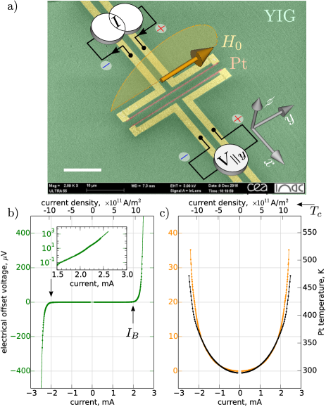
Next, we investigate the implications of these electrical properties for the non-local experiments Cornelissen et al. (2016), where one monitors the transport properties between two parallel metal wires deposited on top of YIG. More precisely, one measures the voltage along one wire (the detector) as a current flows through a second wire (the injector). FIG.2a shows a microscopy image of the electrode pattern on top of the YIG. In these lateral devices, the two parallel wires are made of Pt (see two red lines in FIG.2a along the -direction) and the same devices have also been used to investigate the spin conduction properties of YIG. For the lateral device series used herein, the Pt wires are 7 nm thick, 300 nm wide, and 30 m long. Since different Pt wires (thickness and length) have been deposited between different samples, comparison of the results should be done by juxtaposing data obtained with identical current densities (provided in the upper scale). The total resistance of the Pt wire at room temperature is k, corresponding to a Pt resistivity of 27.3 .cm. Although the analysis below concentrates on a particular lateral device, whose Pt wires are separated by a gap of 0.4 m, these measurements have been also performed on a multitude of other devices patterned on two different LPE YIG film batch of similar thickness. In the following, we shall explicitly clarify the effects, that are generic to the YIG films. In our measurement setup the current is injected in the device only during 10 ms pulses using a 10% duty cycle. This pulse method is very important in order to limit heating of the YIG and substrate. The increase of resistance of the Pt wire is monitored during the pulse. The result is shown in FIG.2c (right axis), where we have plotted as a function of the current , with the coefficient K specific to Pt Landolt and Börnstein (1970). The result is shown in FIG.2c using black dots. For information purposes, we have also marked on the plot the position of the Curie temperature . In the following, we shall assume that the local YIG temperature is identical to that of the Pt (i.e. assuming negligible Kapitza resistance 111A more precise analysis should consider the possibility that the temperature differs between the YIG and the Pt.). One can use this plot to estimate the temperature effects on the electrical properties. At mA, which corresponds to current density of about Am2 circulating in the Pt injector wire, the temperature of the YIG has increased to about 370 K during the pulse. At this temperature, the YIG resistivity drops into the sub- range according to FIG.1a, which corresponds to a sheet resistance of about 50 G. Considering now the lateral aspect ratio of the device, this amounts to an electrical resistance of YIG of the order of the G between the two wires. The leakage current inside the Pt detector wire, whose impedance is about 6 orders of magnitude smaller than the one of YIG, starts thus to reach the sub-nA range, which is comparable to the induced currents produced by inverse spin Hall effects.
To resolve this effect in our lateral device, we propose to measure the non-local voltage with the magnetization set precisely parallel to the Pt wire. This configuration switches off completely any sensitivity to spin conduction. To align the magnetization with the wire, an external in-plane magnetic field of kOe is applied along the -direction as shown in FIG.2. The induced offset voltage is decomposed in two contributions: b) one , which is odd in current (green) and the other c) , which is even in current (orange).
We first concentrate on the odd contribution of the offset shown in green in FIG.2b. For the odd offset it is always observed that, within our convention of biasing the high/low binding posts of the current source and voltmeter in the same direction (cf. and polarities in FIG.2a), the sign of is positive for positive current and negative for negative current. It implies that , which means that the voltage drop is produced by dissipation. One should emphasize that this sign is opposite to the voltage produced by the inverse spin Hall effect (cf. FIG.2e in ref.Thiery et al. (2017)). On the figure scale, we observe that the odd offset increases abruptly above mA (corresponding to a YIG temperature of 370 K). This offset actually follows an exponential growth as shown in the insert using a semi-logarithmic scale. The solid line in FIG.2b is a fit with an exponential increase , where the temperature is extracted from the Pt resistance (cf. black dots in FIG.2c). From the fit, we extract the local band-gap eV, which is the same as that extracted from the resistivity. We then evaluate quantitatively the expected signal from current leakage through the YIG. At mA, when the temperature of the YIG reaches K, the YIG resistivity drops to about . Considering the equivalent circuit, this will produce a difference of potential of 50V on the detector circuit, which is consistent with the observed signal. This confirms that the odd offset voltage in our non-local device is purely produced by the decrease of the YIG electrical resistivity. Note that this offset voltage drops very quickly with decreasing current pulse amplitude. As shown in the insert of FIG.2b, it decreases by an order of magnitude, when mA (corresponding to a YIG temperature of K). At this level, the offset starts to become of the same order of magnitude as the spin signal in these devices. We have thus indicated by an arrow in FIG.2b, mA (i.e. current densities of approximately Am2), the threshold current at which the electrical leakage starts to become important in the spin transport experiments.
We then move to the even contribution of the offset shown in orange in FIG.2c. One observes that this contribution always follows the Joule heating of the Pt wire, so it is linked to the induced thermal gradient. It is ascribed to thermoelectric effects produced by a small temperature difference at the two PtAl contacts of the detector circuit. This difference is produced by small resistance asymmetries along the Pt wire length, which induce one end to heat more than the other end. Considering the Seebeck coefficient of PtAl, of 3.5V/K Landolt and Börnstein (1970), the offset measured at mA, corresponds to a temperature difference of less than 3 ∘C between the top and bottom contact electrodes, while the wire is being heated by almost 70 ∘C. These asymmetries in the temperature difference are expected to vary from one device to the other and this is precisely what is observed: the ratio between the even contribution of the offset and the temperature increase of the Pt wire fluctuates and even changes sign randomly between different lateral devices.
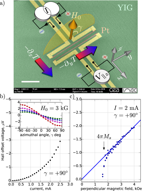
Although the offset voltage is independent of the external magnetic field direction when the latter is rotated in-plane, it is in principle sensitive to the out-of-plane component through the Hall effect. This transverse transport in YIG is attracting a lot of interest and several recent papers address the issue of transverse magnon transport effects in magnetic materials, such as the magnon Hall effect Onose et al. (2010) or the magnon planar Hall effect Liu et al. (2017). The sensitivity to magnons effects can be eliminated from the measurements by keeping the magnetization vector in the -plane containing the interface normal and the length of the Pt stripe and thus this configuration selects only the transverse transport properties carried by the electrical charge. To extract the Hall voltage, we shall only consider the -signal, defined as the difference between the measured voltage for two opposite polarities of the external magnetic field , . This signal would be also sensitive to the spin Seebeck effects if the YIG magnetization had a non-vanishing projection along the -axis Thiery et al. (2017). The insert of FIG.3b shows the angular dependence as a function of the azimuthal angle, , being defined in FIG.3a. On all the devices, we observe that the -dependence of the -signal is: maximum when the field is applied along the -direction; odd in magnetic field; and negative when . Moreover, the -signal increases with both increasing current density and increasing external magnetic field. It is worth to note at this point that the offset voltage produced by the perpendicular magnetic field is about two orders of magnitude smaller than that of the in-plane direction. The observed quadratic dependence with in FIG.3b suggests that this signal should be associated to Joule heating and thus to particle flux induced by thermal gradients. The observed linear dependence with in FIG.3c suggests that this signal should be associated to a normal Hall effect and not to an anomalous Hall effect linked to . Indeed a fit of the high field data leads to a straight line that intercepts the origin, while anomalous Hall effect would have lead to a finite intercept. One also observes in FIG.3c a departure from this linear behavior below the saturation field. This is because, below saturation, a component of the magnetization could point in the -direction, hereby switching on the sensitivity to the spin Seebeck effect, which is a stronger positive signal in these devices.
Next we discuss more in details the potential origin of the -signal. First, as noted in the previous paragraph, the source is the incoming flux of charge carriers produced by a thermal gradient. This gradient is in the -direction, through the potent Joule heating of the injector. There is in principle an electrical voltage produced in the -direction associated with this incoming flux through the electrical Nernst effect. Our device geometry effectively shunts both contacts with a relatively low impedance Pt wire, acting as a voltage divider, which reduces drastically any sensitivity to the Nernst effect. One should mention at this point the recently reported spin Nernst effect Meyer et al. (2017). But this signal should be maximum when the magnetization is parallel to the -direction, while the signal that we discuss here is maximum when the magnetization is parallel to the -direction. We propose here a different scenario to explain our data. Since our measurement of the even offset in FIG.2c seems to indicate that the two thermocouples provided by the PtAl contacts at both ends of the detector Pt wire are sensitive to temperature difference along the -direction, the Hall offset signal measured in FIG.3 can thus be due to a thermal gradient in the -direction (Righi-Leduc effects Madon et al. (2016)). Although a definite quantitative proof would require some additional measurements, in the following we shall check that this explanation is consistent with the data.
Firstly, this explanation is consistent with the and behavior. Secondly, it also has the correct sign. Since the -signal is negative for , this implies that and have the same sign when the field is positive. This is the signature of a -type doping in agreement with FIG.1b. Concerning the amplitude of these thermal gradients, at mA, we evaluate the temperature of the YIG underneath the injector and the detector by measuring the value of the Kittel frequency at these two positions using -BLS spectroscopy. Comparing these values between FIG.4a and FIG.4b of ref.Thiery et al. (2017) allows to estimate the decrease of spontaneous magnetization under the injector (-290 G) and the detector (-110 G). If one uses the fact that YIG magnetization decreases by 4G/∘C in this temperature range, we find that at mA the temperature of the YIG underneath the injector has increased by +73∘C, while the temperature of the YIG underneath the detector has increased by +27∘C. The fact that these values agree with the increase of temperature of the Pt resistance confirms that the Kapitza resistance is probably small. Using the gap of 0.4m between the 2 Pt wires as the area where the thermal gradient along occurs, we find that C/m. Using a value of cm2/(Vsec) for the Hall mobility, this would produce a transverse gradient of ∘C/m in a perpendicular magnetic field of 3 kG. Recalling that the length of the Pt wires is 30m long, this would produce a voltage of 2V, using the thermoelectric coefficient of PtAl. So in the end, the expected signal amplitude is of the same order of magnitude as the Hall offset measured at mA.
In summary, we have shown that high quality YIG thin films grown by LPE behave as a large gap semiconductor at high temperature due to the presence of a small amount of impurities inside the YIG. In our case, we observe that the resistivity drops to about at K. These results are important for non-local transport exploring the spin conductivity, especially in cases where the YIG is subject to a large amount of defects like in amorphous materials, or when improper cooling of the sintered product leads to the additional formation of Ohmic grain boundaries. In non-local transport devices, these electrical properties are responsible for the abrupt emergence of an odd offset voltage at large current densities as well as a temperature gradient along the wire proportional to the perpendicular component of the magnetic field. These results emphasize the importance of reducing drastically the Joule heating by using a pulse method, when investigating spin transport in YIG in the strong out-of-equilibrium regime. For our devices, these electrical properties start to become non-negligible for spin transport studies, when the YIG temperature is heated K, which corresponds in our case to injecting a current density Am2 in the Pt (or mA for these samples). We add that non-local voltage produced by Ohmic losses in the YIG are easily separated from the non-local voltage produced by spin transport. Firstly, the two signals have opposite polarities. Secondly, only the latter varies with the orientation of the magnetization in-plane, as first demonstrated by the Groeningen group Cornelissen et al. (2016).
Acknowledgements.
This research was supported by the priority program SPP1538 Spin Caloric Transport (SpinCaT) of the DFG and by the program Megagrant 14.Z50.31.0025 of the Russian ministry of Education and Science. VVN acknowledges fellowship from the emergence strategic program of UGA, and Russian program of competitive growth of KFU.References
- Valenzuela and Tinkham (2006) S. O. Valenzuela and M. Tinkham, Nature 442, 176 (2006).
- Kajiwara et al. (2010) Y. Kajiwara, K. Harii, S. Takahashi, J. Ohe, K. Uchida, M. Mizuguchi, H. Umezawa, H. Kawai, K. Ando, K. Takanashi, S. Maekawa, and E. Saitoh, Nature 464, 262 (2010).
- Miron et al. (2011) I. M. Miron, K. Garello, G. Gaudin, P.-J. Zermatten, M. V. Costache, S. Auffret, S. Bandiera, B. Rodmacq, A. Schuhl, and P. Gambardella, Nature 476, 189 (2011).
- Rojas-Sánchez et al. (2013) J.-C. Rojas-Sánchez, L. Vila, G. Desfonds, S. Gambarelli, J. P. Attané, J. M. D. Teresa, C. Magén, and A. Fert, Nature Comm. 4, 2944 (2013).
- Wang et al. (2011) Z. Wang, Y. Sun, M. Wu, V. Tiberkevich, and A. Slavin, Phys. Rev. Lett. 107, 146602 (2011).
- Padrón-Hernández et al. (2011) E. Padrón-Hernández, A. Azevedo, and S. M. Rezende, Appl. Phys. Lett. 99, 192511 (2011).
- Chumak et al. (2012) A. V. Chumak, A. A. Serga, M. B. Jungfleisch, R. Neb, D. A. Bozhko, V. S. Tiberkevich, and B. Hillebrands, Appl. Phys. Lett. 100, 082405 (2012).
- Hahn et al. (2013) C. Hahn, G. de Loubens, O. Klein, M. Viret, V. V. Naletov, and J. Ben Youssef, Phys. Rev. B 87, 174417 (2013).
- d’Allivy Kelly et al. (2013) O. d’Allivy Kelly, A. Anane, R. Bernard, J. Ben Youssef, C. Hahn, A. H. Molpeceres, C. Carretero, E. Jacquet, C. Deranlot, P. Bortolotti, R. Lebourgeois, J.-C. Mage, G. de Loubens, O. Klein, V. Cros, and A. Fert, Appl. Phys. Lett. 103, 082408 (2013).
- Hamadeh et al. (2014) A. Hamadeh, O. d’Allivy Kelly, C. Hahn, H. Meley, R. Bernard, A. H. Molpeceres, V. V. Naletov, M. Viret, A. Anane, V. Cros, S. O. Demokritov, J. L. Prieto, M. Muñoz, G. de Loubens, and O. Klein, Phys. Rev. Lett. 113, 197203 (2014).
- Collet et al. (2016) M. Collet, X. de Milly, O. d’Allivy Kelly, V. Naletov, R. Bernard, P. Bortolotti, J. Ben Youssef, V. Demidov, S. Demokritov, J. Prieto, M. Muñoz, V. Cros, A. Anane, G. de Loubens, and O. Klein, Nature Commun. 7, 10377 (2016).
- Lauer et al. (2016) V. Lauer, D. A. Bozhko, T. Brächer, P. Pirro, V. I. Vasyuchka, A. A. Serga, M. B. Jungfleisch, M. Agrawal, Y. V. Kobljanskyj, G. A. Melkov, C. Dubs, B. Hillebrands, and A. V. Chumak, Appl. Phys. Lett. 108, 012402 (2016).
- Du et al. (2017) C. Du, T. van der Sar, T. X. Zhou, P. Upadhyaya, F. Casola, H. Zhang, M. C. Onbasli, C. A. Ross, R. L. Walsworth, Y. Tserkovnyak, and et al., Science 357, 195–198 (2017).
- Wesenberg et al. (2017) D. Wesenberg, T. Liu, D. Balzar, M. Wu, and B. L. Zink, Nat Phys advance online publication, (2017).
- Thiery et al. (2017) N. Thiery, A. Draveny, V. V. Naletov, L. Vila, J.-P. Attané, G. de Loubens, M. Viret, N. Beaulieu, J. Ben Youssef, V. E. Demidov, S. O. Demokritov, A. N. Slain, V. S. Tiberkevich, A. Anane, P. Bortolotti, V. Cros, and O. Klein, ArXiv e-prints (2017), arXiv:1702.05226 [cond-mat.mtrl-sci] .
- Safranski et al. (2017) C. Safranski, I. Barsukov, H. K. Lee, T. Schneider, A. A. Jara, A. Smith, H. Chang, K. Lenz, J. Lindner, Y. Tserkovnyak, and et al., Nature Communications 8 (2017), 10.1038/s41467-017-00184-5.
- Lauer et al. (2016) V. Lauer, M. Schneider, T. Meyer, C. Dubs, P. Pirro, T. Brächer, F. Heussner, B. Lägel, V. I. Vasyuchka, A. A. Serga, B. Hillebrands, and A. V. Chumak, ArXiv e-prints (2016), arXiv:1612.07305 [cond-mat.mes-hall] .
- Larsen and Metselaar (1976) P. K. Larsen and R. Metselaar, Phys. Rev. B 14, 2520 (1976).
- Metselaar and Larsen (1978) R. Metselaar and P. K. Larsen, Proceedings of the International School of Physics Enrico Fermi 70, 417 (1978), phys. Magn.
- Lal et al. (1982) H. B. Lal, B. K. Verma, and V. Ram Yadav, Journal of Materials Science 17, 3317 (1982).
- Petrov et al. (1986) A. Petrov, G. Denisov, and V. Zhukovskii, Inorg. Mater. (Engl. Transl.); (United States) 22:4 (1986).
- Sirdeshmukh et al. (1998) L. Sirdeshmukh, K. Krishna Kumar, S. Bal Laxman, A. Rama Krishna, and G. Sathaiah, Bulletin of Materials Science 21, 219–226 (1998).
- Modi and Sharma (2014) K. Modi and P. Sharma, Radiation Effects and Defects in Solids 169, 723 (2014), http://dx.doi.org/10.1080/10420150.2014.918130 .
- Sparks (1969) M. Sparks, Physical Review Letters 22, 1111 (1969).
- Fang et al. (2017) Z. Fang, A. Mitra, A. L. Westerman, M. Ali, C. Ciccarelli, O. Cespedes, B. J. Hickey, and A. J. Ferguson, Applied Physics Letters 110, 092403 (2017), http://dx.doi.org/10.1063/1.4977490 .
- Kang et al. (2005) Y.-M. Kang, S.-H. Wee, S.-I. Baik, S.-G. Min, S.-C. Yu, S.-H. Moon, Y.-W. Kim, and S.-I. Yoo, Journal of Applied Physics 97, 10A319 (2005), http://dx.doi.org/10.1063/1.1855460 .
- Wang et al. (2013) H. L. Wang, C. H. Du, Y. Pu, R. Adur, P. C. Hammel, and F. Y. Yang, Phys. Rev. B 88, 100406 (2013).
- Sun et al. (2012) Y. Sun, Y.-Y. Song, H. Chang, M. Kabatek, M. Jantz, W. Schneider, M. Wu, H. Schultheiss, and A. Hoffmann, Appl. Phys. Lett. 101, 152405 (2012).
- Onbasli et al. (2014) M. C. Onbasli, A. Kehlberger, D. H. Kim, G. Jakob, M. Kläui, A. V. Chumak, B. Hillebrands, and C. A. Ross, APL Mater. 2, 106102 (2014).
- Hauser et al. (2016) C. Hauser, T. Richter, N. Homonnay, C. Eisenschmidt, M. Qaid, H. Deniz, D. Hesse, M. Sawicki, S. G. Ebbinghaus, and G. Schmidt, Scientific Reports 6 (2016), 10.1038/srep20827.
- Dubs et al. (2017) C. Dubs, O. Surzhenko, R. Linke, A. Danilewsky, U. Brückner, and J. Dellith, Journal of Physics D: Applied Physics 50, 204005 (2017).
- Bullock and Epstein (1970) D. C. Bullock and D. J. Epstein, Applied Physics Letters 17, 199 (1970), http://dx.doi.org/10.1063/1.1653364 .
- Cornelissen et al. (2016) L. J. Cornelissen, K. J. H. Peters, G. E. W. Bauer, R. A. Duine, and B. J. van Wees, Phys. Rev. B 94, 014412 (2016).
- Landolt and Börnstein (1970) H. Landolt and R. Börnstein, Group III, Condensed Matter, Numerical data and functional relationship in Science and technology (Springer, Berlin, 1970).
- Note (1) A more precise analysis should consider the possibility that the temperature differs between the YIG and the Pt.
- Onose et al. (2010) Y. Onose, T. Ideue, H. Katsura, Y. Shiomi, N. Nagaosa, and Y. Tokura, Science 329, 297 (2010).
- Liu et al. (2017) J. Liu, L. J. Cornelissen, J. Shan, T. Kuschel, and B. J. van Wees, Phys. Rev. B 95, 140402 (2017).
- Meyer et al. (2017) S. Meyer, Y.-T. Chen, S. Wimmer, M. Althammer, T. Wimmer, R. Schlitz, S. Geprägs, H. Huebl, D. Ködderitzsch, H. Ebert, and et al., Nature Materials (2017), 10.1038/nmat4964.
- Madon et al. (2016) B. Madon, D. C. Pham, J.-E. Wegrowe, D. Lacour, M. Hehn, V. Polewczyk, A. Anane, and V. Cros, Phys. Rev. B 94, 144423 (2016).