Depletion-mode Quantum Dots in Intrinsic Silicon
Abstract
We report the fabrication and electrical characterization of depletion-mode quantum dots in a two-dimensional hole gas (2DHG) in intrinsic silicon. We use fixed charge in a SiO2/Al2O3 dielectric stack to induce a 2DHG at the Si/SiO2 interface. Fabrication of the gate structures is accomplished with a single layer metallization process. Transport spectroscopy reveals regular Coulomb oscillations with charging energies of meV and meV for the few- and many-hole regimes, respectively. This depletion-mode design avoids complex multilayer architectures requiring precision alignment, and allows to adopt directly best practices already developed for depletion dots in other material systems. We also demonstrate a method to deactivate fixed charge in the SiO2/Al2O3 dielectric stack using deep ultraviolet light, which may become an important procedure to avoid unwanted 2DHG build-up in Si MOS quantum bits.
In order to perform sufficient operations in a quantum computerDiVincenzo (1995), the quantum bits are required to be long-lived. Group IV semiconductors not only hold promise for very long spin coherence times Tyryshkin et al. (2011); Steger et al. (2012); Veldhorst et al. (2014); Muhonen et al. (2014), but also may take advantage from the scalability provided by semiconductor industry. These benefits have attracted much attention Liu et al. (2008); Zwanenburg et al. (2009); Lim et al. (2009); Simmons et al. (2009); Higginbotham et al. (2014); Borselli et al. (2015) to quantum dots (QDs) in group IV material systems as a framework for a solid-state scalable spin-based quantum computerLoss and DiVincenzo (1998). Recently hole transport in QDs became a subject of particular interest, both experimentalLi et al. (2013); Ares et al. (2013); Spruijtenburg et al. (2013); Li et al. (2015); Voisin et al. (2016); Watzinger et al. (2016); Brauns et al. (2016) and theoreticalSalfi et al. (2016); Hung et al. (2017); Marcellina et al. (2017), since the hyperfine interaction is strongly suppressed, while the spin-orbit coupling enables all-electrical spin manipulationNowack et al. (2007) boosting scalability of hole-based qubits. However, enabled electrical spin control makes them vulnerable to charge noise that leads to dephasing and decoherence of the spin states. Elimination of electrically active defects at the location of the QDs is essential to extend the hole spin coherence time. In Si planar QDs, nanometer-size Coulomb islands are electrostatically defined in a gated MOSFET-type structure at the Si/SiO2 interface. The disorder and defects at this interface can be detrimental to the robustness and reliability of hole spin qubits.
Y
A low-temperature (400 ∘C) hydrogen treatment is traditionally used to deactivate defects at the Si/SiO2 interface. One way to implement it is based on hydrogen diffusion during atomic layer deposition (ALD) of Al2O3 thin films Dingemans et al. (2010). We have successfully used this approach recentlySpruijtenburg et al. (2016) to improve the quality of silicon QDs. This method can lead to building up of a negative fixed charge in Al2O3Hoex et al. (2008), strong enough to induce 2DHG at the Si/SiO2 interface. Here we demonstrate a method to neutralize it and give a hint on the mechanism of this phenomenon. Besides, here we utilize to create depletion-mode QDs in intrinsic silicon.
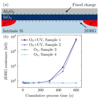
To show the effect of negative buildup, we use intrinsic Si ( kcm) with predefined ohmic contacts to highly doped p++ silicon areas and 7 nm of thermally grown SiO2 as a substrate. After deposition of 5 nm of Al2O3 by thermal ALD (TMA/H2O, at =250 ∘C) on the substrate, we anneal it in an argon atmosphere (100 Pa, 30 minutes, =400 ∘C). Fig. 1(a) shows a schematic cross-section of the fabricated substrate. builds up in Al2O3 during annealing. Although there is no consensus on its origin, one possible explanation Simon et al. (2015) is that initial growth regime of a few first ALD cycles being non-stoichiometric provides an excess of oxygen atoms and deep charge traps at the SiO2/Al2O3 interface. Electrons fill these traps during annealing, providing a net number of fixed charges per unit area in the rangeSimon et al. (2015); Hoex et al. (2008) of cm-2. This is enough to induce the two-dimensional hole gas (2DHG) at the Si/SiO2 interface in our devices and short ohmic contacts at temperatures down to a few mK.
Besides using to create depletion-mode QDs, we also present a method to neutralize it and eliminate the corresponding 2DHG using deep ultraviolet light (UV). We expose annealed samples in a UV ozone generator (wavelength =254 nm) and measure the 2-point resistance of 2DHG between ohmic contacts ex situ at =4.2 K. Fig. 1(b) shows after 9 iterative steps of exposure up to a total cumulative process time of 600 s. After exposure to UV light and O3 two different samples (“”,“” symbols in Fig. 1(b)) demonstrate the same behavior. After approximately 10 minutes of cumulative exposure to UV light and O3, the restores back to the resistance common for intrinsic Si at this temperature. In contrast, two control samples only exposed to O3 (“Y”,“ Y ” symbols in Fig. 1(b)) demonstrate a slight decrease in . A possible explanation of the observed neutralization is that high-energy UV radiation promotes diffusion of oxygenGupta et al. (2015) in Al2O3, which improves stoichiometry of the film, eliminating charge traps and the in it, as well as the induced 2DHG. The results in Fig. 1 show that post-anneal UV exposure is an essential treatment of the enhancement-mode QDs in intrinsic Si, as it allows to avoid short circuits via 2DHG in hole- and ambipolar-QDsSpruijtenburg et al. (2016); Brauns et al. (2017).
At the same time, we propose below to take advantage of the induced 2DHG. We see that the negative present in Al2O3 after annealing induces a 2DHG without any applied gate voltage. This 2DHG, combined with only a single layer of gate electrodes, is the ingredient necessary to create depletion-mode type QDs, similar to devices created in GaAs/AlGaAsCiorga et al. (2000) or Si/SiGe heterostructuresSimmons et al. (2007); Zajac et al. (2016). The following paragraphs describe a proof-of-principle of the creation of such devices in intrinsic Si, and feature two gate designs that can be further optimized to realize single-hole occupation.
A depletion-mode quantum dot relies on the presence of a conducting state without applying voltages to electrodes. The already present 2DHG is locally depleted by positive voltages on the gate electrodes to form the tunnel barriers required for a QD Ciorga et al. (2000). Here we deposit metallic gates on the substrate shown in Fig. 1(a) using electron-beam lithography, e-beam evaporation, and lift-off techniques. An extra layer of 5 nm Al2O3 is deposited on the devices using ALD to protect gates during the annealing stepBrauns et al. (2017); Spruijtenburg et al. (2017).
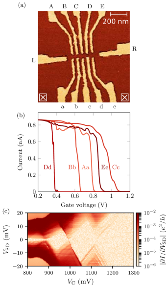
First, we test the capability of the gate electrodes to locally deplete the 2DHG and pinch off the channel. Fig. 2(a) shows the device “ABC” that consists of 10 electrodes coming in from the top and bottom. The electrodes at the far-left (L) and far-right (R) are present in the design for extra tunability. Each vertical pair of the electrodes, designated the same upper and lower case letter, forms a gate. Fig. 2(b) shows current-voltage characteristics of individual gates of the device “ABC”. We can see that conduction through the channel can be turned off completely by applying sufficient voltages on gate. This voltage depletes the 2DHG not only underneath a pair of top and bottom electrodes but also in between them. By tuning an applied voltage we can thus form a tunnel barrier between that pair.
Now using a couple of these tunnel barriers we will form a QD between the two adjacent gates Bb and Cc. The expectation is that, due to the gate geometry, the gaps between B and C as well as b and c are fully depleted except the very center of the structure where an island is formed. At the same time the gaps between the top and bottom electrodes remain sufficiently conducting to act as two tunnel barriers to the formed island. Fig. 2(c) shows the transport spectroscopy of a formed QD. For optimal stability, only the voltage on the electrode C is varied in this measurement. The charging energy of the last visible transition is measured to be 15 meV and is an indication of reaching the single-hole regime, although only a charge sensing experiment can verify single-charge occupation Elzerman et al. (2003); Yang et al. (2011); Yamaoka et al. (2017). This value is comparable to the charging energy of previously obtained results for the last electron in Si Spruijtenburg et al. (2016); Lim et al. (2009); Yang et al. (2013); Lim et al. (2011). The results in Fig. 2 demonstrate that we can form QDs using this approach; the gate design needs further optimizationMalkoc, Stano, and Loss (2016) to improve control of a future spin qubit.
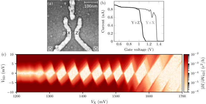
To advance results on Fig. 2, we adapt a proven gate designCiorga et al. (2000) to create the device “XYZ”, shown in Fig. 3(a). To measure current-voltage characteristics of the left and right tunnel barriers we ground one of the bottom gates Z or X and sweep voltage together on the two other gates i.e. X and Y or Z and Y, respectively. Fig. 3(c) shows transport spectroscopy of a QD formed between the gates. Well-defined non-distorted Coulomb diamonds with charging energies of meV demonstrate the formation of a many-hole QD. This corresponds to an electrostatically defined Coulomb island with a size of 6070 nm based on a parallel plate capacitor model, which is close to the lithographical dimensions of the QD (75 nm). These results show that we can form a robust hole-QD using a straightforward process and simple design. Further reduction of the lithographical dimensions of this design, which is already optimized for spin-qubit performanceMalkoc, Stano, and Loss (2016), may allow reaching the few-hole regime.
To summarize, we have demonstrated that we can eliminate a 2DHG induced by fixed charge in Al2O3 by a deep-UV light treatment. This phenomenon potentially has a great impact on the MOS electron-QD community as many groups are starting to use ALD and might unintentionally induce a 2DHG in their samples with no possibility to detect it. Another important application for this technology is fine tuning of the bandgap bending that can improve coupling of nuclear spins to a microwave resonatorPla et al. (2016). Finally, hybrid-mode devices, where ALD-oxide will replace source/drain accumulation gates of the enhancement-mode devices to induce a 2DHG, simplifying fabrication and increasing the yield, can utilize the same phenomenon.
We have also shown transport characteristics of a single-layer depletion-mode hole-QD. Transport measurements indicate that we can fabricate QDs in the many-hole regime as well as QDs showing signs of the few-hole regime, where the last visible charge-transition has a charging energy meV.
Initially depletion-mode QDs were made in group IV semiconductors by doping, incompatible with long coherence times, or by use of epitaxial heterostructures. The design and device, as presented here, make for a very simple system to create depletion-mode QDs in undoped Si without the need for accumulation gates. The well-defined Coulomb diamonds when a single quantum dot is formed are promising, and optimization can push this design even further. This optimization should take care to absorb the lessons learned in previous designsCiorga et al. (2000), and are an easy path to tunable arrays of QDsZajac et al. (2016) reaching single-hole occupation. Our fabrication method reliably passivates electrically active defects by hydrogen annealing, reducing charge noise, the primary source of qubit decoherenceBermeister, Keith, and Culcer (2014). An additional advantage of a single-layer depletion-mode device is that it avoids damage from any electron-beam lithographyKim, Tyryshkin, and Lyon (2017) in the areas where the dots are actively formed. The open nature of the design means that future experiments could more easily couple external sources of light into the structure, for example, to optically address individual ions in siliconYin et al. (2013); Morse et al. (2017) and transfer quantum states between distant nodes of a quantum internetKimble (2008). Conversely, by using positive fixed charge in another gate dielectric stack, e.g. SiO2/HfO2, one could create electron-based depletion-mode QDsSimon et al. (2015). Given these features, the depletion-mode design has its place alongside the enhancement-mode designLim et al. (2009); Liu et al. (2008), and could prove extremely useful in experiments in intrinsic Si.
Acknowledgements.
We thank Matthias Brauns and Joost Ridderbos for fruitful discussions. We acknowledge technical support by A.A.I. Aarnink and J.W. Mertens. This work is part of the research program “Atomic physics in the solid state” with project number 14167, which is (partly) financed by the Netherlands Organisation for Scientific Research (NWO).References
- DiVincenzo (1995) D. P. DiVincenzo, Science 270, 255 (1995).
- Tyryshkin et al. (2011) A. M. Tyryshkin, S. Tojo, J. J. L. Morton, H. Riemann, N. V. Abrosimov, P. Becker, H.-J. Pohl, T. Schenkel, M. L. W. Thewalt, K. M. Itoh, and S. A. Lyon, Nature Materials 11, 143 (2011).
- Steger et al. (2012) M. Steger, K. Saeedi, M. L. W. Thewalt, J. J. L. Morton, H. Riemann, N. V. Abrosimov, P. Becker, and H.-J. Pohl, Science 336, 1280 (2012).
- Veldhorst et al. (2014) M. Veldhorst, J. C. C. Hwang, C. H. Yang, A. W. Leenstra, B. de Ronde, J. P. Dehollain, J. T. Muhonen, F. E. Hudson, K. M. Itoh, A. Morello, and A. S. Dzurak, Nature Nanotechnology 9, 981 (2014).
- Muhonen et al. (2014) J. T. Muhonen, J. P. Dehollain, A. Laucht, F. E. Hudson, R. Kalra, T. Sekiguchi, K. M. Itoh, D. N. Jamieson, J. C. McCallum, A. S. Dzurak, and A. Morello, Nature Nanotechnology 9, 986 (2014).
- Liu et al. (2008) H. W. Liu, T. Fujisawa, Y. Ono, H. Inokawa, A. Fujiwara, K. Takashina, and Y. Hirayama, Physical Review B 77, 073310 (2008).
- Zwanenburg et al. (2009) F. A. Zwanenburg, C. E. W. M. van Rijmenam, Y. Fang, C. M. Lieber, and L. P. Kouwenhoven, Nano Letters 9, 1071 (2009).
- Lim et al. (2009) W. H. Lim, F. A. Zwanenburg, H. Huebl, M. Möttönen, K. W. Chan, A. Morello, and A. S. Dzurak, Applied Physics Letters 95, 242102 (2009).
- Simmons et al. (2009) C. B. Simmons, M. Thalakulam, B. M. Rosemeyer, B. J. Van Bael, E. K. Sackmann, D. E. Savage, M. G. Lagally, R. Joynt, M. Friesen, S. N. Coppersmith, and M. A. Eriksson, Nano Letters 9, 3234 (2009).
- Higginbotham et al. (2014) A. P. Higginbotham, F. Kuemmeth, M. P. Hanson, A. C. Gossard, and C. M. Marcus, Physical Review Letters 112 (2014), 10.1103/PhysRevLett.112.026801.
- Borselli et al. (2015) M. G. Borselli, K. Eng, R. S. Ross, T. M. Hazard, K. S. Holabird, B. Huang, A. A. Kiselev, P. W. Deelman, L. D. Warren, I Milosavljevic, A. E. Schmitz, M. Sokolich, M. F. Gyure, and A. T. Hunter, Nanotechnology 26, 375202 (2015).
- Loss and DiVincenzo (1998) D. Loss and D. P. DiVincenzo, Physical Review A 57, 120 (1998).
- Li et al. (2013) R. Li, F. E. Hudson, A. S. Dzurak, and A. R. Hamilton, Applied Physics Letters 103, 163508 (2013).
- Ares et al. (2013) N. Ares, V. N. Golovach, G. Katsaros, M. Stoffel, F. Fournel, L. I. Glazman, O. G. Schmidt, and S. De Franceschi, Physical Review Letters 110, 046602 (2013).
- Spruijtenburg et al. (2013) P. C. Spruijtenburg, J. Ridderbos, F. Mueller, A. W. Leenstra, M. Brauns, A. A. I. Aarnink, W. G. van der Wiel, and F. A. Zwanenburg, Applied Physics Letters 102, 192105 (2013).
- Li et al. (2015) R. Li, F. E. Hudson, A. S. Dzurak, and A. R. Hamilton, Nano Letters 15, 7314 (2015).
- Voisin et al. (2016) B. Voisin, R. Maurand, S. Barraud, M. Vinet, X. Jehl, M. Sanquer, J. Renard, and S. De Franceschi, Nano Letters 16, 88 (2016).
- Watzinger et al. (2016) H. Watzinger, C. Kloeffel, L. Vukušić, M. D. Rossell, V. Sessi, J. Kukučka, R. Kirchschlager, E. Lausecker, A. Truhlar, M. Glaser, A. Rastelli, A. Fuhrer, D. Loss, and G. Katsaros, Nano Letters 16, 6879 (2016).
- Brauns et al. (2016) M. Brauns, J. Ridderbos, A. Li, W. G. van der Wiel, E. P. A. M. Bakkers, and F. A. Zwanenburg, Applied Physics Letters 109, 143113 (2016).
- Salfi et al. (2016) J. Salfi, M. Tong, S. Rogge, and D. Culcer, Nanotechnology 27, 244001 (2016).
- Hung et al. (2017) J.-T. Hung, E. Marcellina, B. Wang, A. R. Hamilton, and D. Culcer, Physical Review B 95, 195316 (2017).
- Marcellina et al. (2017) E. Marcellina, A. R. Hamilton, R. Winkler, and D. Culcer, Physical Review B 95 (2017), 10.1103/PhysRevB.95.075305.
- Nowack et al. (2007) K. C. Nowack, F. H. L. Koppens, Y. V. Nazarov, and L. M. K. Vandersypen, Science 318, 1430 (2007).
- Dingemans et al. (2010) G. Dingemans, W. Beyer, M. C. M. van de Sanden, and W. M. M. Kessels, Applied Physics Letters 97, 152106 (2010).
- Spruijtenburg et al. (2016) P. C. Spruijtenburg, S. V. Amitonov, F. Mueller, W. G. van der Wiel, and F. A. Zwanenburg, Scientific Reports 6, 38127 (2016).
- Hoex et al. (2008) B. Hoex, J. J. H. Gielis, M. C. M. v. d. Sanden, and W. M. M. Kessels, Journal of Applied Physics 104, 113703 (2008).
- Simon et al. (2015) D. K. Simon, P. M. Jordan, T. Mikolajick, and I. Dirnstorfer, ACS Applied Materials & Interfaces 7, 28215 (2015).
- Gupta et al. (2015) S. Gupta, S. Hannah, C. Watson, P. Šutta, R. Pedersen, N. Gadegaard, and H. Gleskova, Organic Electronics 21, 132 (2015).
- Brauns et al. (2017) M. Brauns, S. V. Amitonov, P.-C. Spruijtenburg, and F. A. Zwanenburg, arXiv:1709.07699 [cond-mat] (2017), arXiv: 1709.07699.
- Ciorga et al. (2000) M. Ciorga, A. S. Sachrajda, P. Hawrylak, C. Gould, P. Zawadzki, S. Jullian, Y. Feng, and Z. Wasilewski, Physical Review B 61, R16315 (2000).
- Simmons et al. (2007) C. B. Simmons, M. Thalakulam, N. Shaji, L. J. Klein, H. Qin, R. H. Blick, D. E. Savage, M. G. Lagally, S. N. Coppersmith, and M. A. Eriksson, Applied Physics Letters 91, 213103 (2007).
- Zajac et al. (2016) D. Zajac, T. Hazard, X. Mi, E. Nielsen, and J. Petta, Physical Review Applied 6, 054013 (2016).
- Spruijtenburg et al. (2017) P. C. Spruijtenburg, S. V. Amitonov, W. G. van der Wiel, and F. A. Zwanenburg, arXiv:1709.08866 [cond-mat] (2017), arXiv: 1709.08866.
- Elzerman et al. (2003) J. Elzerman, R. Hanson, J. Greidanus, L. Willems van Beveren, S. De Franceschi, L. Vandersypen, S. Tarucha, and L. Kouwenhoven, Physical Review B 67 (2003), 10.1103/PhysRevB.67.161308.
- Yang et al. (2011) C. H. Yang, W. H. Lim, F. A. Zwanenburg, and A. S. Dzurak, AIP Advances 1, 042111 (2011).
- Yamaoka et al. (2017) Y. Yamaoka, K. Iwasaki, S. Oda, and T. Kodera, Japanese Journal of Applied Physics 56, 04CK07 (2017).
- Yang et al. (2013) C. H. Yang, A. Rossi, R. Ruskov, N. S. Lai, F. A. Mohiyaddin, S. Lee, C. Tahan, G. Klimeck, A. Morello, and A. S. Dzurak, Nature Communications 4 (2013), 10.1038/ncomms3069.
- Lim et al. (2011) W. H. Lim, C. H. Yang, F. A. Zwanenburg, and A. S. Dzurak, Nanotechnology 22, 335704 (2011).
- Malkoc, Stano, and Loss (2016) O. Malkoc, P. Stano, and D. Loss, Physical Review B 93 (2016), 10.1103/PhysRevB.93.235413.
- Pla et al. (2016) J. J. Pla, A. Bienfait, G. Pica, J. Mansir, F. A. Mohiyaddin, A. Morello, T. Schenkel, B. W. Lovett, J. J. L. Morton, and P. Bertet, arXiv preprint arXiv:1608.07346 (2016).
- Bermeister, Keith, and Culcer (2014) A. Bermeister, D. Keith, and D. Culcer, Applied Physics Letters 105, 192102 (2014).
- Kim, Tyryshkin, and Lyon (2017) J.-S. Kim, A. M. Tyryshkin, and S. A. Lyon, Applied Physics Letters 110, 123505 (2017).
- Yin et al. (2013) C. Yin, M. Rancic, G. G. de Boo, N. Stavrias, J. C. McCallum, M. J. Sellars, and S. Rogge, Nature 497, 91 (2013).
- Morse et al. (2017) K. J. Morse, R. J. S. Abraham, A. DeAbreu, C. Bowness, T. S. Richards, H. Riemann, N. V. Abrosimov, P. Becker, H.-J. Pohl, M. L. W. Thewalt, and S. Simmons, Science Advances 3, e1700930 (2017).
- Kimble (2008) H. J. Kimble, Nature 453, 1023 (2008).