Stacking change in MoS2 bilayers induced by interstitial Mo impurities
Abstract
We use a theoretical approach to reveal the electronic and structural properties of molybdenum impurities between MoS2 bilayers. We find that interstitial Mo impurities are able to reverse the well-known stability order of the pristine bilayer, because the most stable form of stacking changes from AA’(undoped) into AB (doped). The occurrence of Mo impurities in different positions shows their split electronic levels in the energy gap, following octahedral and tetrahedral crystal fields. The energy stability is related to the accommodation of Mo impurities compacted in hollow sites between layers. Other less stable configurations for Mo dopants have larger interlayer distances and band gaps than those for the most stable stacking. Our findings suggest possible applications such as exciton trapping in layers around impurities, and the control of bilayer stacking by Mo impurities in the growth process.
Today
I Introduction
The recent isolation of new 2D materials, such as hexagonal boron nitride (h-BN) Novoselov et al. (2005), black phosphorus Castellanos-Gomez et al. (2014), and particularly transition metal dichalcogenides (TMDCs) Yang et al. (1991) have attracted considerable attention thanks to their interesting physical, chemical, electronic, optical, and mechanical properties Splendiani et al. (2010); Chhowalla et al. (2013); Wang et al. (2012); Kośmider et al. (2013); Radisavljevic et al. (2011); Lopez-Sanchez et al. (2013); Zeng et al. (2012); Castellanos-Gomez et al. (2012). Among TMDCs, MoS2 is being used as prototype in several different applications, such as photovoltaic cells, photocatalysts, electronic nanodevices, and energy storage and conversion materials Zhiming M. Wang (2014). In structural terms, a layer of MoS2 has Mo centers coordinated with six sulfur ligands in a trigonal prismatic arrangement Liu et al. (2015); Roldán et al. (2014), following a hexagonal lattice of alternating Mo and S atoms, as seen from above. TMDCs nanostructures can then be produced by stacking several MoS2 layers through weak van der Waals interactions. It is noteworthy that the number of layers and their stacking arrangement largely modify the electronic properties of the MoS2 semiconductor Ataca et al. (2011); López-Suárez et al. (2016); Yuan et al. (2016); He et al. (2014); Yan et al. (2016a). For instance, the MoS2 monolayer shows a direct band gap, compared with the indirect band gap of MoS2 bulk Mahatha et al. (2012); Zhao et al. (2013); Kośmider and Fernández-Rossier (2013); Padilha et al. (2014). The stacking in the MoS2 bilayer alters the band gap, which can then be engineered not only by strain Dong et al. (2014); Sharma et al. (2014), but also by sliding Levita et al. (2014) and twisting the MoS2 layers Liu et al. (2014). Thus, the control of the MoS2 bilayer stacking is relevant when considering different applications in future devices.

The electronic and magnetic properties of MoS2 monolayers and bilayers are also tuned by defects, such as vacancies and adatoms Chang et al. (2014); Huang et al. (2013); Wang et al. (2015). Most of the adatom impurities considered within MoS2 layers are in groups IA and VIIA, or transition metal atoms. The adatoms in the interlayer space have interesting effects, such as n- or p-type doping, induced magnetic moments Wang et al. (2014); He et al. (2010); Lu and Leburton (2014), and structural phase transitions Pandey et al. (2016). Although some early photoelectron spectroscopy experiments appeared to show Mo atoms embedded between MoS2 layers Fives et al. (1992), current experiments using low-temperature STM show Mo impurities between bilayers Wan et al. (2013). However, the effects of intrinsic Mo impurity atoms on the electronic and structural properties of MoS2 bilayers with different stackings are still largely unexplored.
We present a theoretical study of the structural and electronic properties of the MoS2 bilayer considering Mo atoms as intrinsic impurities, placed at different positions within the interlayer region in a diluted regime. Using density functional with van der Waals calculations from first principles, we relax the structures and study their electronic properties. We find that the intrinsic Mo impurities in the interlayer region produce some interesting behaviors, namely (i) a change in the stability order with respect to the pristine bilayer, energetically favoring the AB stacking over the AA’, (ii) impurity states in the band gap region, and (iii) an increase in the distance between layers. The structural and electronic modifications induced by the impurities could be employed as electron and exciton-like traps He et al. (2013); Castellanos-Gomez et al. (2013), and the change in stacking produced by the Mo impurities could also be useful to fine-tune the stacking during the growing process Liu et al. (2014); Yan et al. (2016b).
II Model and Computational Details
A Mo doped MoS2 bilayer is described using density functional of van der Waals (vdW-DF) calculations with the SIESTA method Soler et al. (2002). To describe the core electrons, we consider norm-conserving relativistic ab-initio pseudopotentials in the Troullier Martins form Troullier and Martins (1991), including nonlinear core corrections for inner d-electrons Louie et al. (1982). The exchange and correlation energy are calculated by the non-local vdW-DF, using the parametrization proposed by Dion et al Dion et al. (2004), taking into account the exchange energy modification included by Cooper (C09) Cooper (2010). To include impurities, the structures of the MoS2 bilayers are extended to a MoS2 supercell, using periodic boundary conditions. A k-grid of Monkhorst-Pack is used to sample the Brillouin zone. A vacuum region in the z-direction, of at least 20 Å avoids interactions with periodic images. The structures were relaxed until the force in each atom was less than eV/Å.
We first consider the most stable configurations of the pristine MoS2 bilayer, namely the AA’ and the AB configurations. In AA’ stacking, the hexagons in each layer are superposed in such a way that the molybdenum atoms of the bottom layer are located just below the sulfur atoms in the top layer, and vice-versa. For AB stacking the hexagons in each layer are shifted with the sulfur atoms of the bottom layer beneath the hollow sites of top layer, and the molybdenum atoms in the top layer over the molybdenum atoms in the bottom layer He et al. (2014), as shown schematically in Fig. 1. In our calculations we found an energy difference between these stackings of E - EAB = meV per atom, in good agreement with previous DFT calculations He et al. (2014); Yan et al. (2016a); Yang et al. (2014).
We then include Mo atoms as intrinsic impurities within the interlayer region for both bilayer stackings at different inequivalent positions, as shown in Fig. 1. The Mo impurity is labeled as Moimp. The initial absorption sites for Mo within the MoS2 bilayer are assumed to follow Mo sites in MoS2 monolayers Komsa and Krasheninnikov (2015); Hong et al. (2017). For AA’ stacking, we have (i) a hollow site (H) in the center of the two hexagonal rings formed by the Mo and sulfur atoms belonging to the MoS2 bilayer, (ii) a top site (T) just above a sulfur atom of the bottom layer, and (iii) a bridge site (B) between two sulfur atoms of the MoS2 bilayer. In the AB stacking we also included (iv) the top site (T’) on the S atom.

The MoS2 bilayer structures with the impurity in the interlayer region are fully relaxed, to allow the optimized lattice parameters and atomic coordinates to be obtained. The binding energy can then be calculated using:
where is the total energy of the MoS2 bilayer with the impurity, is the energy of the corresponding final pristine MoS2 bilayer (either AA’ or AB), and is the energy for the isolated Moimp atom.
III Results and Discussion
III.1 Energy and Geometry
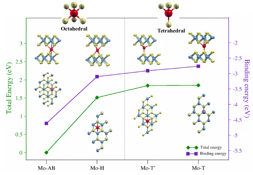
Figure 2 shows the total and binding energies for the different stackings and impurity positions. The binding energies are negative, which indicates that the Mo impurity atoms are indeed adsorbed in the interlayer region of the MoS2 bilayer. The binding and total energies exhibit the same trend in terms of stability. The results in increasing order of stability shows that in the presence of the interlayer Moimp, the Mo-AB bilayer configuration is the most energetically favorable. This configuration has AB stacking with the Moimp superposed with two Mo atoms as seen from above. Note that the Mo-AB configuration is reached from the input that has the Moimp placed at the bridge (B) position in the AA’ stacking.
The next most favorable configuration is Mo-H, with the Moimp in the hollow position, in which the bilayer structure maintains the AA’ stacking. The Mo-H case is less stable than Mo-AB by about eV. On the right hand side, the configurations labeled Mo-T’(or T) for AB (or AA’) stackings are energetically close, and the least stable.
We classify the relaxed configurations according to how the Moimp is related structurally to its neighboring sulfur atoms Kertesz and Hoffmann (1984); Benavente et al. (2002). The Mo-AB and Mo-H configurations form octahedral sites around the Moimp. These configurations have a coordination number of six, corresponding to the six neighboring sulfur atoms. The Mo-T and Mo-T’ configurations for the Moimp form a tetrahedral structure with a coordination number of four, therefore, the sulfur atoms in the top and bottom layers form a tetrahedral site for the Moimp. These octahedral and tetrahedral environments are shown schematically at the top of Fig. 2. It is noteworthy that regardless of the final stacking, octahedral configurations are the most stable.
III.2 Electronic Properties
Results showing the band structures and the local density of states (LDOS) projected in space, for some of the considered configurations, are presented in Fig. 3. We focus on the impurity in-gap states near the Fermi energy introduced by the Moimp atom, indicated by the areas enclosed by orange rectangles. The band structures of the most stable structures show three distinctive in-gap states, joined in two groups, labeled as regions 1 and 2 with degeneracies of one and two, respectively. Although the Moimp in these two configurations presents an octahedral sulfur environment, the in-gap bands present slightly different dispersive behavior. In region 1, the band for the Mo-AB case is more dispersive than the corresponding band for the Mo-H configuration, which is almost flat. The states in region 1 mainly have d orbital character, as shown in the LDOS of panels (d) and (e). Note that in region 1, the surrounding region of the impurity for the Mo-AB case has some hybridization with bilayer orbitals, which is not observed for the Mo-H case. In region 2 of the Mo-AB case, there are two energy bands which are mainly non-bonding Moimp d orbitals with the neighboring sulfur atoms, as shown in the LDOS in panels (d) and (e). By comparing the Mo-AB and Mo-H configurations, the stability order can be associated with the widening of the bands in regions 1 and 2 and to the displacement of the bands in region 2 to lower energies in the Mo-AB configuration.
The band structures in the Mo-AB and Mo-H configurations are spin-compensated and related to the impurity in an octahedral sulfur environment. We now focus on the Mo-T and Mo-T’ cases. These two configurations have similar energy band structures and are found to have close energies. Both systems exhibit spin polarized behavior with a total magnetic moment of 2 , which is determined by a similar Moimp tetrahedral environment. In particular for the Mo-T configuration, the spin up and spin down components of the spatial resolved LDOS are shown in Fig. 3 panel (f). The state in region 1 has a d orbital character; however, it is above the Fermi level. The LDOS of the lower impurity states, the up states in region 3 and the spin down component in region 2 are nearly equal, depleting the LDOS in the Moimp-S bond direction as in the Mo-AB case. However, the states responsible for the spin polarization in the T and T’ configurations are the spin up d-orbitals in region 2, which are along the Moimp-S bonds. We also find that the LDOS is localized not only on the Moimp, but also on one of the MoS2 layers. This layer asymmetry indicates that doping by electrons or holes could spatially differentiate between the two layers in the MoS2 bilayer, a finding that could be of use in optoelectronic applications Hong et al. (2014); Kośmider and Fernández-Rossier (2013).
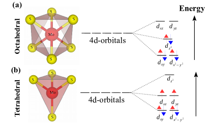
The electronic structure for the impurity level states is best understood using crystal field theory. We analyze the ligand field splitting for the Moimp d-orbitals produced by the interactions with the sulfur ligands for the octahedral and tetrahedral sites. The bonding and non-bonding interactions of d-orbitals for octahedral and tetrahedral sites are in agreement with the energy level scheme shown in Fig. 4. We consider the z-axis perpendicular to the layers and the x and y axes in the in-plane layer. In the octahedral environment for the Mo-AB and Mo-H configurations, the sulfur ligands overlap less with the in-plane dxy and d orbitals, these orbitals are therefore non-bonding and have the lowest energy. The d orbital remains non-bonding at an intermediate energy, interacting less with the sulfur atoms. We next find that the dxz and dyz orbitals are more strongly directed and interact with the sulfur atoms along Moimp-S bonds, lying at higher energies. In the case of tetrahedral environment fo Mo-T’ and Mo-T, shown in Fig. 4(b), the dxy and d orbitals behave similarly to the octahedral structure; however, the dxz and dyz orbitals exchange roles with the d orbital. Thus, the d orbital in the tetrahedral environment interacts more with the sulfur ligands increasing its energy, as shown for region 1 of Fig. 3(c) and (f) in the Mo-T case. The level filling help to explain why the tetrahedral cases have spin polarization, and a total magnetization of 2 , as shown by the arrow counting.
We now consider the gap changes in the bulk bands, shown in gray in Fig. 3, and induced by the Moimp. It is well known that band gaps calculated using GGA infra-estimate the values produced in experiments, so we discuss differences in magnitude gaps. The layer-gap is indicated by the energy difference between the HOMO-LUMO bulk bands at the -point 111Note that the two-gap scenario of the original unit cell is reduced to a direct gap at the -point due to k-space folding.. The energy gaps of the pristine MoS2 layers are correlated with the interlayers distances. We check that the gap and distances for the AB pristine stacking are eV smaller and Å shorter than the values for the AA’ pristine case. The layer-gaps and the interlayer separation including Moimp show larger values in comparison with the pristine cases. Among the Mo doped systems, the most stable Mo-AB case has the smaller layer-gap and the shortest interlayer separation. The layer-gap is eV above the AB-pristine, and the interlayer separation is Å larger than that of AB-pristine. The layer-gap values for the Mo-H and the T and T’ increase from the Mo-AB case by eV and by eV respectively. These gap differences are somewhat correlated with the difference between layer-layer distances, 0.5 Å, between the Mo-AB and Mo-H cases, a value that increases up to Å for the T(T’) configurations. The increase in the layer-band-gap with interlayer distance is explained by a weaker interlayer coupling.
The interlayer distances in the proximity of the impurity are between and Å larger than those far from it, which indicates the role of local strain. Furthermore, experiments prove than the band gap of bilayer TMDCs can be controlled by strain Castellanos-Gomez et al. (2013); San-Jose et al. (2016); Feng et al. (2012). We propose that the electronic and structural modifications around the impurity could be used in a similar way to electronic confinement for embedded quantum dots. Current experimental techniques employing cross-sectional scanning transmission electron microscope analysis in encapsulated TMDC materials can provide evidence of impurity species being trapped in the interstitial region Rooney et al. (2017). This effect thus has potential applications for optoelectronic devices as exciton traps around Mo-doped bilayers. A number of different experimental techniques can be used to corroborate our theoretical predictions, for instance angle-resolved photoemission spectroscopy and cross-sectional scanning transmission electron microscope analysis Brauer et al. (1999); Rooney et al. (2017).
III.3 Stacking change
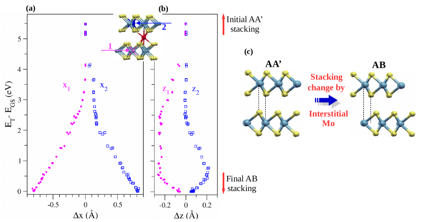
Another possible implication of our results is that transition metal ions could be used to engineer the stacking between TMDC bilayers and to tune their electronic properties. In the Mo-AB and Mo-H configurations, the Moimp is located within sulfur ligands forming octahedral sites. In these two configurations, the Moimp presents structural differences in the relative position respect to the nearest Mo atoms, belonging to the top and bottom MoS2 layers. The Moimp bonding produces a stacking change in Mo-AB related to the total energy decrease. The interlayer Mo-Mo distance around the impurity is smaller around 0.1 Å than the interlayer distance away from the impurity. The shorter distance promotes the hybridization of the impurity states with the layer states increasing the dispersion of the in-gap impurity states.
Figure 5 (a-b) shows the total energy change versus the relative displacement in the x and z directions, for two distant Mo atoms during the relaxation steps, starting with the AA’ stacking. We find that the total energy drops until it reaches the reference ground state energy. The displacements in the z-direction show that the layers are breathing towards the ground-state AB stacking. The energy at the maximum turning point is eV, a value that reflects the barrier to be overcome by shifting the layers. In Fig. 5(c), we schematize the stacking change from AA’ to AB mediated by the presence of a Moimp atom, the stability gain produced by the Moimp favors AB stacking. DFT calculations controlling the sliding of pristine bilayers yield a similar energetic profile, but in the reverse direction to the Mo-doped bilayers Peng et al. (2014).
IV Final Remarks
We studied the structural and electronic properties of a MoS2 bilayer with intrinsic Mo impurities within the interlayer region. We find that the most stable configuration is Mo-AB, with an energy gain above the van der Waals interaction because the Mo impurity levels strongly hybridize with the nearest atoms. Note that pristine bilayers have AA’ stacking as the ground state. A change in the stacking stability order from AA’ to AB is observed to be induced by impurities, with the corresponding variation in energy gap. Thus, it is possible to engineer the stacking between TMDC bilayers during the growth process, enabling their electronic properties to be fine-tuned. The states and deformations induced by impurities could also be used for electronic confinement applications in optoelectronic devices, based on exciton/electron trapping.
Acknowledgments
This work was part financed by a Fondecyt grant 1140388 and Anillo Bicentenario de Ciencia y Tecnología, Conicyt grant Act-1204. J.W. González and A. Ayuela acknowledge the financial support of the Spanish Ministry of Economy and Competitiveness MINECO projects FIS2013-48286-C02-01-P and FIS2016-76617-P, the Basque Government under the ELKARTEK project(SUPER), and the University of the Basque Country grant No. IT-756-13. N. Cortés acknowledge support from the Conicyt grant, No 21160844 and the hospitality of CFM-MPC and DIPC. The authors are indebted to Prof. B. Harmon, L. Chico and T. Alonso-Lanza for their helpful discussions, we also acknowledge the technical support of the DIPC computer center.
References
- Novoselov et al. (2005) K. Novoselov, D. Jiang, F. Schedin, T. Booth, V. Khotkevich, S. Morozov, and A. Geim, Proceedings of the National Academy of Sciences of the United States of America 102, 10451 (2005).
- Castellanos-Gomez et al. (2014) A. Castellanos-Gomez, L. Vicarelli, E. Prada, J. O. Island, K. Narasimha-Acharya, S. I. Blanter, D. J. Groenendijk, M. Buscema, G. A. Steele, J. Alvarez, et al., 2D Materials 1, 025001 (2014).
- Yang et al. (1991) D. Yang, S. J. Sandoval, W. Divigalpitiya, J. Irwin, and R. Frindt, Physical Review B 43, 12053 (1991).
- Splendiani et al. (2010) A. Splendiani, L. Sun, Y. Zhang, T. Li, J. Kim, C.-Y. Chim, G. Galli, and F. Wang, Nano Letters 10, 1271 (2010).
- Chhowalla et al. (2013) M. Chhowalla, H. S. Shin, G. Eda, L.-J. Li, K. P. Loh, and H. Zhang, Nature Chemistry 5, 263 (2013).
- Wang et al. (2012) Q. H. Wang, K. Kalantar-Zadeh, A. Kis, J. N. Coleman, and M. S. Strano, Nature Nanotechnology 7, 699 (2012).
- Kośmider et al. (2013) K. Kośmider, J. W. González, and J. Fernández-Rossier, Physical Review B 88, 245436 (2013).
- Radisavljevic et al. (2011) B. Radisavljevic, A. Radenovic, J. Brivio, i. V. Giacometti, and A. Kis, Nature Nanotechnology 6, 147 (2011).
- Lopez-Sanchez et al. (2013) O. Lopez-Sanchez, D. Lembke, M. Kayci, A. Radenovic, and A. Kis, Nature nanotechnology 8, 497 (2013).
- Zeng et al. (2012) H. Zeng, J. Dai, W. Yao, D. Xiao, and X. Cui, Nature nanotechnology 7, 490 (2012).
- Castellanos-Gomez et al. (2012) A. Castellanos-Gomez, M. Poot, G. A. Steele, H. S. J. van der Zant, N. Agraït, and G. Rubio-Bollinger, Advanced Materials 24, 772 (2012).
- Zhiming M. Wang (2014) E. Zhiming M. Wang, MoS2 Materials, Physics, and Devices, vol. 1 of 21 (Springer International Publishing, Springer International Publishing Switzerland, 2014), 1st ed.
- Liu et al. (2015) G.-B. Liu, D. Xiao, Y. Yao, X. Xu, and W. Yao, Chemical Society Reviews 44, 2643 (2015).
- Roldán et al. (2014) R. Roldán, J. A. Silva-Guillén, M. P. López-Sancho, F. Guinea, E. Cappelluti, and P. Ordejón, Annalen der Physik 526, 347 (2014).
- Ataca et al. (2011) C. Ataca, M. Topsakal, E. Akturk, and S. Ciraci, The Journal of Physical Chemistry C 115, 16354 (2011).
- López-Suárez et al. (2016) M. López-Suárez, I. Neri, and R. Rurali, Journal of Applied Physics 119, 165105 (2016).
- Yuan et al. (2016) H. Yuan, Z. Liu, G. Xu, B. Zhou, S. Wu, D. Dumcenco, K. Yan, Y. Zhang, S.-K. Mo, P. Dudin, et al., Nano Letters 16, 4738 (2016).
- He et al. (2014) J. He, K. Hummer, and C. Franchini, Physical Review B 89, 075409 (2014).
- Yan et al. (2016a) A. Yan, W. Chen, C. Ophus, J. Ciston, Y. Lin, K. Persson, and A. Zettl, Physical Review B 93, 041420 (2016a).
- Mahatha et al. (2012) S. Mahatha, K. Patel, and K. S. Menon, Journal of Physics: Condensed Matter 24, 475504 (2012).
- Zhao et al. (2013) W. Zhao, R. M. Ribeiro, M. Toh, A. Carvalho, C. Kloc, A. Castro Neto, and G. Eda, Nano Letters 13, 5627 (2013).
- Kośmider and Fernández-Rossier (2013) K. Kośmider and J. Fernández-Rossier, Physical Review B 87, 075451 (2013).
- Padilha et al. (2014) J. Padilha, H. Peelaers, A. Janotti, and C. Van de Walle, Physical Review B 90, 205420 (2014).
- Dong et al. (2014) L. Dong, A. M. Dongare, R. R. Namburu, T. P. O’Regan, and M. Dubey, Applied Physics Letters 104, 053107 (2014).
- Sharma et al. (2014) M. Sharma, A. Kumar, P. Ahluwalia, and R. Pandey, Journal of Applied Physics 116, 063711 (2014).
- Levita et al. (2014) G. Levita, A. Cavaleiro, E. Molinari, T. Polcar, and M. Righi, The Journal of Physical Chemistry C 118, 13809 (2014).
- Liu et al. (2014) K. Liu, L. Zhang, T. Cao, C. Jin, D. Qiu, Q. Zhou, A. Zettl, P. Yang, S. G. Louie, and F. Wang, Nature Communications 5, 4966 (2014).
- Chang et al. (2014) J. Chang, S. Larentis, E. Tutuc, L. F. Register, and S. K. Banerjee, Applied Physics Letters 104, 141603 (2014).
- Huang et al. (2013) Z. Huang, G. Hao, C. He, H. Yang, L. Xue, X. Qi, X. Peng, and J. Zhong, Journal of Applied Physics 114, 083706 (2013).
- Wang et al. (2015) X.-Q. Wang, W.-G. Chen, Z.-L. Zhu, and Y. Jia, Acta Metallurgica Sinica (English Letters) 28, 793 (2015).
- Wang et al. (2014) Y. Wang, B. Wang, R. Huang, B. Gao, F. Kong, and Q. Zhang, Physica E: Low-dimensional Systems and Nanostructures 63, 276 (2014).
- He et al. (2010) J. He, K. Wu, R. Sa, Q. Li, Y. Wei, et al., Applied Physics Letters 96, 082504 (2010).
- Lu and Leburton (2014) S.-C. Lu and J.-P. Leburton, Nanoscale Research Letters 9, 1 (2014).
- Pandey et al. (2016) M. Pandey, P. Bothra, and S. K. Pati, The Journal of Physical Chemistry C 120, 3776 (2016).
- Fives et al. (1992) K. Fives, I. McGovern, R. McGrath, R. Cimino, G. Hughes, A. McKinley, and G. Thornton, Journal of Physics: Condensed Matter 4, 5639 (1992).
- Wan et al. (2013) W. Wan, H. Li, H. Huang, S. L. Wong, L. Lv, Y. Gao, and A. T. S. Wee, ACS nano 8, 970 (2013).
- He et al. (2013) K. He, C. Poole, K. F. Mak, and J. Shan, Nano letters 13, 2931 (2013).
- Castellanos-Gomez et al. (2013) A. Castellanos-Gomez, R. Roldán, E. Cappelluti, M. Buscema, F. Guinea, H. S. van der Zant, and G. A. Steele, Nano letters 13, 5361 (2013).
- Yan et al. (2016b) A. Yan, W. Chen, C. Ophus, J. Ciston, Y. Lin, K. Persson, and A. Zettl, Physical Review B 93, 041420 (2016b).
- Soler et al. (2002) J. M. Soler, E. Artacho, J. D. Gale, A. García, J. Junquera, P. Ordejón, and D. Sánchez-Portal, Journal of Physics: Condensed Matter 14, 2745 (2002).
- Troullier and Martins (1991) N. Troullier and J. L. Martins, Physical Review B 43, 1993 (1991).
- Louie et al. (1982) S. G. Louie, S. Froyen, and M. L. Cohen, Physical Review B 26, 1738 (1982).
- Dion et al. (2004) M. Dion, H. Rydberg, E. Schröder, D. C. Langreth, and B. I. Lundqvist, Physical Review Letters 92, 246401 (2004).
- Cooper (2010) V. R. Cooper, Physical Review B 81, 161104 (2010).
- Yang et al. (2014) S. Yang, J. Kang, Q. Yue, and K. Yao, The Journal of Physical Chemistry C 118, 9203 (2014).
- Komsa and Krasheninnikov (2015) H.-P. Komsa and A. V. Krasheninnikov, Physical Review B 91, 125304 (2015).
- Hong et al. (2017) J. Hong, Y. Pan, Z. Hu, D. L, C. Jin, W. Ji, J. Yuan, and Z. Zhang, Nano Letters 17, 3383 (2017).
- Kokalj (1999) A. Kokalj, Journal of Molecular Graphics and Modelling 17, 176 (1999).
- Kertesz and Hoffmann (1984) M. Kertesz and R. Hoffmann, Journal of the American Chemical Society 106, 3453 (1984).
- Benavente et al. (2002) E. Benavente, M. Santa Ana, F. Mendizábal, and G. González, Coordination Chemistry Reviews 224, 87 (2002).
- Hong et al. (2014) X. Hong, J. Kim, S.-F. Shi, Y. Zhang, C. Jin, Y. Sun, S. Tongay, J. Wu, Y. Zhang, and F. Wang, Nature Nanotechnology 9, 682 (2014).
- Momma and Izumi (2011) K. Momma and F. Izumi, Journal of Applied Crystallography 44, 1272 (2011).
- San-Jose et al. (2016) P. San-Jose, V. Parente, F. Guinea, R. Roldán, and E. Prada, Physical Review X 6, 031046 (2016).
- Feng et al. (2012) J. Feng, X. Qian, C.-W. Huang, and J. Li, Nature Photonics 6, 866 (2012).
- Rooney et al. (2017) A. P. Rooney, A. Kozikov, A. N. Rudenko, E. Prestat, M. J. Hamer, F. Withers, Y. Cao, K. S. Novoselov, M. I. Katsnelson, R. V. Gorbachev, et al., Nano Letters (2017).
- Brauer et al. (1999) H. Brauer, H. Starnberg, L. Holleboom, H. Hughes, and V. Strocov, Journal of Physics: Condensed Matter 11, 8957 (1999).
- Peng et al. (2014) T. Peng, G. Huai-Hong, Y. Teng, and Z. Zhi-Dong, Chinese Physics B 23, 106801 (2014).