Unified mechanism of the surface Fermi level pinning in III-As nanowires
Abstract
Fermi level pinning at the oxidized (110) surfaces of III-As nanowires (GaAs, InAs, InGaAs, AlGaAs) is studied. Using scanning gradient Kelvin probe microscopy, we show that the Fermi level at oxidized cleavage surfaces of ternary AlxGa1-xAs (0x0.45) and GaxIn1-xAs (0x1) alloys is pinned at the same position of 4.80.1 eV with regard to the vacuum level. The finding implies a unified mechanism of the Fermi level pinning for such surfaces. Further investigation, performed by Raman scattering and photoluminescence spectroscopy, shows that photooxidation of the AlxGa1-xAs and GaxIn1-xAs nanowires leads to the accumulation of an excess arsenic on their crystal surfaces which is accompanied by a strong decrease of the band-edge photoluminescence intensity. We conclude that the surface excess arsenic in crystalline or amorphous forms is responsible for the Fermi level pinning at oxidized (110) surfaces of III-As nanowires.
- PACS numbers
-
73.20.At.
pacs:
73.20.AtI Introduction
Compound III-As semiconductors (where III atoms are Ga, In, Al) and their ternary alloys, owing to a direct band structure and high carrier mobility, are prospective materials for high electron mobility transistors (HEMT) Mimura et al. (1980), as well as for a large number of optoelectronic devicesFaist et al. (1998); Huffaker et al. (1998). In the last decade, following the general trend to reduce the device sizes down to the nanometer scale, III-As nanowires (NWs) began to be employed for device engineering Bryllert et al. (2006); Saxena et al. (2013); Colombo et al. (2009). In addition to the advantageous essential properties of III-As materials, these nanostructures have their own beneficial features which could be used in nano- and optoelectronics. In particular, the III-As nanowires can be grown on silicon substrates, which facilitates their compatibility with silicon-based device structures Gudiksen et al. (2002); Mårtensson et al. (2004). Also, these nanowires possess an increased light absorption and can be employed, therefore, in the fabrication of solar cells with increased efficiency Krogstrup et al. (2013). However, conventional oxidized surfaces of III-As compounds have a high density of surface states that is related, generally, to surface defects Cowley and Sze (1965). These states are responsible for the surface Fermi level pinning, formation of the near- surface depletion layer, and surface recombination. Owing to the high surface/volume ratio, these surface-induced, negative effects, for III-As nanowires are anticipated to be drastically enhanced. For example, the Fermi level mid-gap pinning that occurs in low-doped GaAs and AlGaAs NWs can totally switch off the conductivity along the nanowire, as well as the photoluminescence Chang et al. (2012). Fixation of the Fermi level in the conduction band known for InAs surfaces facilitates formation of the ohmic contact in n-type nanowires, but gives rise to inversion of the channel conductivity in p-type nanowires Li et al. (2007). It is clear that a comprehensive understanding of the pining induced phenomena is of fundamental importance and also necessary for the design of device structures based on III-As nanowires. Conventionally, III-As nanowire surfaces are formed by (110) facets. Active surfaces of semiconductor lasers have the same orientation. Fermi level pinning does not occur at clean, cleavage (110) faces of III-As bulk semiconductors, which corresponds to the so-called flat-band condition Mönch (1986). However, even a submonolayer deposition of O, Ga, In, Au, Al, and other elements leads to fixation of the surface Fermi level at a position that differs from its position in a bulk crystal. The surface pinning positions are usually measured relative to the tops of valence or conduction bands. In such coordinates, the pinning positions for III-As semiconductors are independent of the nature of the adsorbed atoms Spicer et al. (1979). As a consequence, the surface states responsible for the pinning are now assigned to intrinsic surface defects. The pinning positions for (110) GaAs are 0.75 eV and 0.55 eV above the valence band for n- and p-type materials, respectively Spicer et al. (1980). For the (110) InAs surface, the Fermi level is fixed at 0.13 eV above the bottom of the conduction band for n- and p-type materials Baier et al. (1986). For AlxGa1-xAs ternary alloys, the Fermi level pinning has been studied much less. Note that despite the long period of investigations, the nature of the surface states responsible for the Fermi level pinning in III-arsenides is still a controversial issue. We study the Fermi level pinning at oxidized surfaces of the III-As nanowires. We determine pinning positions on the cleavage surfaces of the III-As heterostructures and study the behavior of the photoluminescence for III-As nanowires under photooxidation. Based on the obtained results, a unified mechanism for the surface Fermi level pinning in the III-As structures and nanowires is proposed.
II Results and discussion
Experimentally, the pinning positions are determined by scanning gradient Kelvin probe microscopy Dunaevskiy et al. (2011). At each scanning point, this technique measures the surface potential, which is the difference between the work functions of a microscope probe and of a semiconductor surface. The latter value presents the energy gap between the vacuum level and the surface Fermi level. In the case of the cleavage faces of III-As heterostructures, such measurements provide a determination of the pinning position for each heterolayer Usunami et al. (1998). To verify the validity of such measurements, we measured the surface potential values on the cleavage face of a p-i-n GaAs structure. The measurements were performed on naturally oxidized surfaces under atmospheric conditions. Figure 1(a) shows the measured profile of the surface potential value along the cleaved n+ (51018 cm-3)-n (11015)-p+ (51018) layers of the structure. From Fig. 1(a), one can conclude that the energy gap between pinning positions for the p+ and n+ layers was approximately 0.2 eV, which was in agreement with reference Spicer et al. (1980). For the weakly doped intermediate layer, the pinning position occurred approximately in the middle between those found for the p+ layer and the n+ substrate. To study the Fermi level pinning at the (110) surface of ternary AlxGa1-xAs, we used the cleavage face of a laser-diode heterostructure AlxGa1-xAs Vinokurov et al. (2005). The heterostructure was grown on n+ GaAs substrate and consisted of the following layers: +-emitter Al0.4Ga0.6As/ p-waveguide Al0.3Ga0.7As/ p-emitter Al0.4Ga0.6As/, and contact p+-GaAs layer. The profile of the surface potential measured across the heterostructure cleavage face is shown in Fig. 1(b). As was observed in Fig. 1(a), the difference between the pinning positions for p+ and n+ GaAs layers was 0.2 eV. As seen from the Fig. 1(b), the pinning positions for the heavily doped n+ Al0.4Ga0.6As layer and for the heavily doped n+ GaAs substrate were very close. For weakly doped p-AlxGa1-xAs layers, the Fermi level was pinned approximately in the middle between the positions for the n+ and p+ layers.

Approximately 20 heterostructures of AlxGa1-xAs, in which the Al concentration x varied in the range of 0.1-0.4, were studied. For all x values, the gap between the pinning positions for doped n+ and p+ layers did not exceed 0.25 eV, while for the weakly doped layers, the pinning positions occurred near the center of this gap. The pinning positions determined with regard to the vacuum level are plotted in Fig. 2(a). As can be seen, for the (110) surface of AlxGa1-xAs (0x0.45), the Fermi level was fixed near 4.80.1 eV and near 4.90.1 eV for the n-and p-type materials, respectively.
To plot the analogous dependence for oxidized surfaces of n-GaxIn1-xAs (0x1), we analyzed the data published in Refs. Spicer et al. (1980); Baier et al. (1986); Mullin and Wieder (1983). In Fig. 2(b), the blue dots mark the known surface pinning positions for n-InAs (Ref. Baier et al. (1986)), n-Ga0.47In0.53As (Ref. Mullin and Wieder (1983)), and n-GaAs (Ref. Spicer et al. (1980)). All these points occurred again at the same distance of 4.80.1 eV from the vacuum level. A similar result was obtained by Weider who observed that the pinning positions for the components of the GaxIn1-xAs metal - insulator-semiconductor (MIS) structures for all x were also equidistant from the vacuum level Wieder (2003). Thus, the obtained results unambiguously demonstrated that at the oxidized (110) surface of III-As compounds, the Fermi levels were fixed at the same energy position calculated from the vacuum level. One can also observe from Fig. 2(b) that for x0.2, the positions of the Fermi level coincided with the bottom of the conduction band, which corresponded to the so-called flat band condition. This was in agreement with the recent studies on n-GaxIn1-xAs nanowiresSpeckbacher et al. (2016).
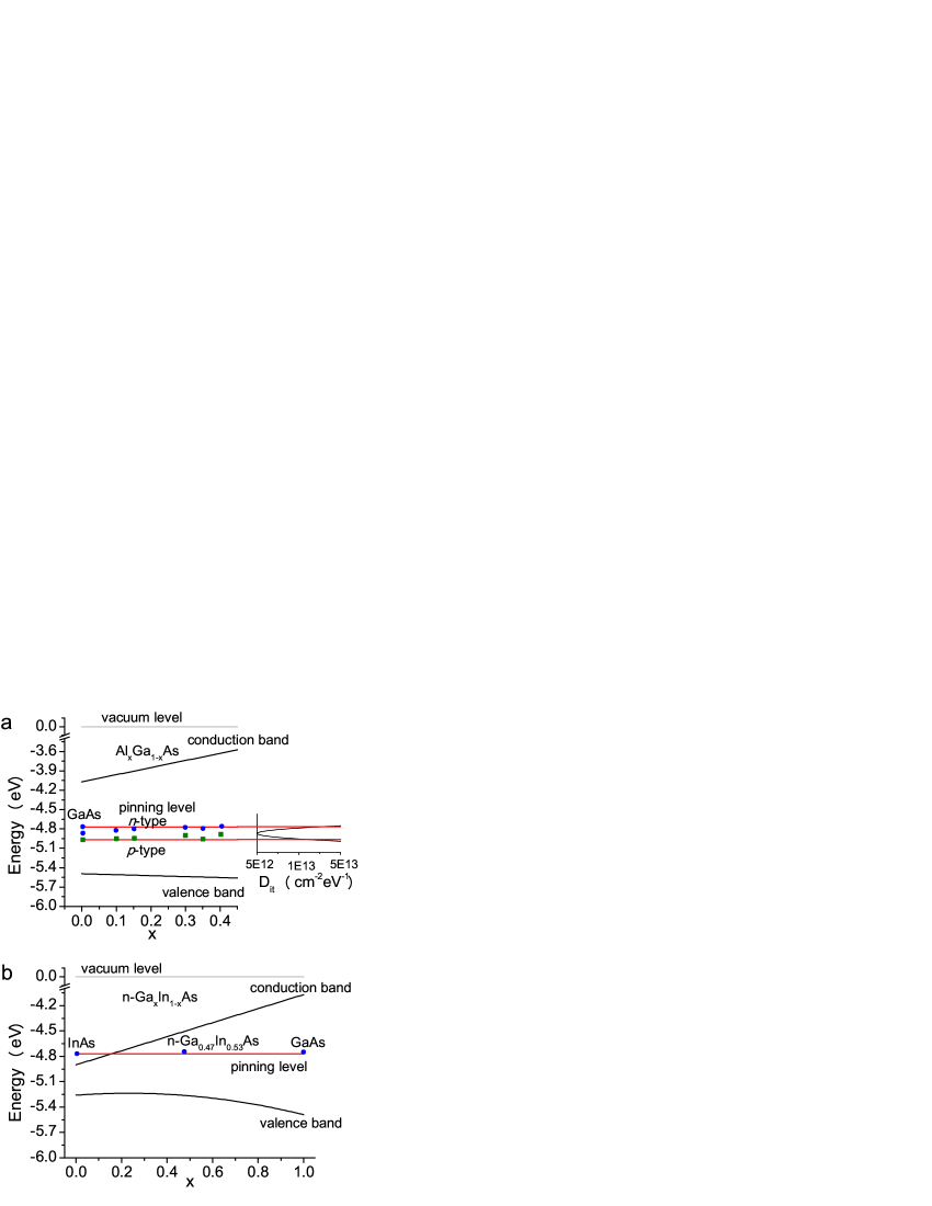
Assuming that the distribution of the surface states density had a ”U” shape shapeHasegawa et al. (2010), we concluded that the minimum of this distribution was at a distance of 4.9 eV from the vacuum level (see Fig. 2(a)), and the width of the distribution did not exceed 0.25 eV. The density of the surface states on the oxidized surface of III-As semiconductors in the distribution minimum has been reported to exceed 1012 cm-2eV-1 (ref. Hasegawa et al. (2010)). Therefore, for low doped p- and n- materials, the Fermi level should be fixed in the vicinity of the distribution minimum. With an increase of the doping level, the surface states at the distribution minimum began to be filled and the Fermi level moved along the distribution curve. As a result, the Fermi level moved upward or downward in the n- and p-type materials, respectively.
The higher the doping level, the larger was the shift of the Fermi level pinning position from the distribution minimum. However, owing to the sharp increase of the surface state density at a distance of 0.1 eV from the distribution minimum, a further increase of the doping level did not shift the pinning position. It should also be noted that the value of the surface states density at the distribution minimum for an oxidized surface can vary from 1012 up to 1013 cm-2eV-1 which can shift the “U” curve in Fig. 2(a) as a whole to the lower or higher state density side of the plot. The presented data unambiguously indicates the existence of a unified mechanism of the Fermi level pinning at oxidized surfaces of III-As semiconductor structures. Indeed, the positions of the surface Fermi level relative to the vacuum level were the same for all investigated III-As compounds and their ternary alloys. We suppose that the Fermi level pinning is caused by atoms of excess arsenic emerging at the III-As semiconductor surfaces under oxidation. Bearing this idea in mind, we studied the photooxidation of GaAs, GaxIn1-xAs, and AlxGa1-xAs nanowires in which, as has already been mentioned, the pinning-induced effects were strongly enhanced. It is known that in air ambient, an intense optical irradiation accelerates the surface oxidation of GaAs and InAs nanowires Yazji et al. (2011); Tanta et al. (2016). A photooxidation-induced decrease of the band-gap photoluminescence (PL) intensity for GaAs nanowires is observed Yazji et al. (2011). We have recently shown that photooxidation leads to the formation of a double layer c-As/ GaOx at the GaAs nanowire surface and it is the c-As layer that contacts the crystal lattice of the nanowire Alekseev et al. (2017).
The photooxidation of III-As NWs was studied using a combination of Raman scattering and photoluminescence (PL) spectroscopy. The former technique was to control chemical composition of the NW surfaces. The experiments were carried out at room temperature (300 K) using Horiba Jobin Yvon T64000 and LabRAM HR spectrometers equipped with a Linkam THMS600 temperature-controlled microscope stage. The measurements were performed with continuous-wave (cw) excitation using the 532 nm laser line of a Nd: YAG laser. We used a Mitutoyo 100× NIR (NA=0.90) long working-distance objective lens to focus the incident beam into a spot of 1 1 m diameter, which was sufficient to measure the PL signal from a separate nanowire transferred to a Si/ SiO2 substrate.
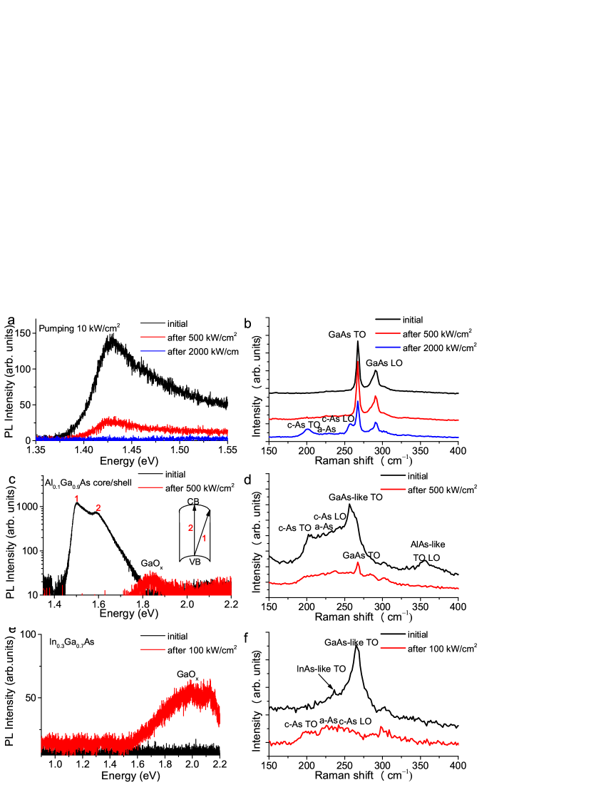
The studied GaAs, Ga0.7In0.3As, and Al0.1Ga0.9As nanowires were grown on Si substrates by the molecular beam epitaxy (MBE) technique using the vapor-liquid solid growth procedure. Gold droplets were used as catalyst. The AlxGa1-xAs nanowires had the core/shell structure Al0.1Ga0.9As/Al0.2Ga0.8AsDubrovskii et al. (2016), in which the first component was the core and the second component was the shell. Scanning electron microscopy images of the NWs are presented in Fig. S1 in the Supplemental material. The experimental procedure was as follows. First, photoluminescence and Raman scattering spectra were measured for the as-received nanowires. Then, the nanowires were exposed to successive one-minute laser irradiations with a power density of 100, 500, and 2000 kW/cm2. After each laser-light exposure, the Raman scattering and PL spectra were measured at a low pumping density of 10 kW/cm2. Figure 3(a) and 3(b) show the spectra obtained for a GaAs nanowire. It can be seen that after 500 kW/cm2beam irradiation, the intensity of the initial PL spectrum (black curve in Fig. 3(a)) decreased by approximately a factor of 10. After the third irradiation (2000 kW/cm2), the band-edge PL was hardly detected. In parallel, the intensive laser irradiation resulted in the appearance and growth of the additional lines in the Raman scattering spectra in the spectral region of 200-260 cm-1 assigned to TO and LO phonons in amorphous and crystalline arsenic Yazji et al. (2011) (see Fig. 3(b)). These results clearly provide evidence that the surface excess arsenic in the crystalline or amorphous forms is the origin of the surface states responsible for surface nonradiative recombination and for the surface Fermi level pinning. These observations agree with the already known results observed on the photooxidation of GaAs nanowires Yazji et al. (2011); Alekseev et al. (2017).
Figure 3(c) and 3(d) show the optical spectra obtained for a Al0.1Ga0.9As/Al0.2Ga0.8As core/shell nanowire. The initial PL spectrum in Fig. 3(c) revealed a doublet whose components at 1.5 and 1.6 eV were assigned to the band-edge PL of the nanowire core (1.6 eV) and to the core-shell transitions (1.5 eV). The initial Raman scattering spectrum, excluding the lines of GaAs-like and AlAs-like TO phonons Jusserand and Sapriel (1981), also exhibited the lines corresponding to the phonons in c- and a-arsenic (see Fig. 3(d)). This arsenic appeared owing to the greater thickness of the natural oxide layer in AlGaAs than that in GaAs Ankudinov et al. (1999). However, the PL intensity of AlGaAs nanowires significantly exceeded the PL of GaAs nanowires, apparently because the NW shell with a higher aluminum content served as a passivation coating for the NW core. Since the NW shell was not fully oxidized, the oxide did not reach the core/shell interface. After irradiation of the nanowire by a beam with the power density of 500 kW/cm2, the band-edge PL was not detected, which indicated that the PL intensity decreased by at least 3 orders of magnitude. At the same time, a weak PL appeared near 1.8 eV, which was apparently related to the formation of the GaOx layerAlekseev et al. (2017). The observed elimination of the band-edge PL intensity arose from the entire oxidation of the core / shell interface. In the Raman scattering spectrum, a weak line associated with a GaAs-like TO phonon remained. It should be noted that after laser irradiation, the broad arsenic-related spectral pedestal remained as well.
Owing to a small diameter and low doping level, the Ga0.7In0.3As nanowire was completely depleted by charge carriers. Therefore, at the pumping density of 10 kW/cm2, the band-edge PL in the nanowire was not observed (Fig. 3(e)). The increase of the pump density resulted in observation of the PL Alekseev et al. (2015), but in ambient conditions, it also produced a complete oxidation of the nanowire. In the initial Raman spectrum shown in Fig. 3(f), InAs-like and GaAs-like TO phonons were visible Hertenberger et al. (2012). After laser irradiation with a power density of 100 kW/cm2, these lines disappeared and, instead, the lines corresponding to crystalline and amorphous arsenic appeared. The weak PL peak observed in Fig. 3(e) in the region 1.7-2.2 eV could be explained by the formation of GaOx /Ga2O3 oxides.
Thus, under photooxidation, the intensity of the band-edge photoluminescence in III-As nanowires decreased with the simultaneous growth of the arsenic layer only on the crystal nanowire surface (see Fig. S2 in the Supplemental material). In addition, for all III-As compounds, fixation of the Fermi level at the oxidized (110) surfaces occurred at the same energy interval from the vacuum level. We propose that the surface arsenic was responsible for the Fermi level pinning in III-As semiconductors. Indeed, it was shown in Ref. Chiang and Spicer (1989) that deposition of As on the clean (110) surface led to pinning of the Fermi level. Annealing of the oxidized surface provided a sublimation of As and led to the unpinning of the Fermi level. Unlike the surface As, the Ga-oxide components of the oxide layers in III-As compounds did not produce the Fermi level pinning. In Ref. Passlack et al. (1997), the Ga2O3 layer was deposited on the GaAs surface and, as a result, the density of mid-gap surface states decreased down to 1010 cm-2eV-1 for the sharp interface between GaAs and Ga2O3.
We now discuss why the surface arsenic created the surface-gap states in III-As. To explain the Fermi level pinning in such compounds, the approaches of the intrinsic defects or of effective work function are conventionally used. In the former approach, initially suggested by Spicer, the electronic states of surface gallium and arsenic vacancies were considered to produce pinning of the surface Fermi level Spicer et al. (1980). Later, more detailed calculations indicated that the mid-gap levels could belong to As-antisite defects whose existence at the oxidized GaAs surface was also confirmed experimentally Stesmans et al. (2013). Very recent studies of the GaAs/oxide interface using density functional theory (DFT) indicated that the mid-gap Fermi level pinning could be caused by more complicated defect complexes, which included an As vacancy (VAs) and two As antisites (AsGa)Colleoni et al. (2015). The latter defect also emerged in the form of a VGa-AsGa complex. As a criticism of the native defects approach, a photo-washing experiment is usually cited. In this experiment, the PL intensity of GaAs samples immersed in water was measured Wilmsen et al. (1988). The PL intensity was observed to increase by an order of magnitude after dissolution of surface arsenic. Moreover, a decrease of the surface states density down to 1011 cm-2eV-1 and the unpinning of the surface Fermi level were demonstrated Offsey et al. (1986). It is unlikely that an aqueous solution could remove surface native defects. Also, the removal of the surface arsenic layer from GaAs by plasma etching was found to produce a decrease of the surface states density Callegari et al. (1989).
The effective work function approach, which was presented by Woodal and Freeouf, assumed that surface chemical reactions induced by oxidation or deposition of metals on the III-As surfaces led to the formation of the surface arsenic layer Woodall and Freeouf (1981). If the effective work function eff is assigned to this As layer, the level pinning position and Schottky barrier height for the n-type materials can be determined as bn = eff-, where is the electron affinity for the III-As semiconductor. There are not too much data on the work function of arsenic. It is known that eff =4.66 eV and 5.1 eV for an amorphous Taft and Apker (1949) and crystalline As layer Middleton and Van Valkenburg (2002), respectively. The theoretically predicted value of eff has been reported as 4.9 eV Michaelson (1977). In our case, the pinning positions in Figure 2(a,b) is in a good agreement with the work function value on the level of 4.8-4.9 eV. However, it is difficult to explain the shift of the Fermi level pinning position by 0.2 eV observed in GaAs when passing from p+ to n+ materials (Fig. 1(a)) using the effective work function approach.
However, the approach using surface native defects remains as partially applicable. Computations in the framework of numerical models indicated that arsenic defect complexes, such as As-As dimer/dangling bond, are good candidates for amphoteric mid-gap defect levels. Such models also describe the abrupt interfaces of GaAs/Al2O3 quite well Robertson et al. (2015). Apparently, the real structure of the natural oxide layer in III-As compounds is quite complex. In particular, surface arsenic can be of a few monolayers of thickness, as has been shown experimentally Alekseev et al. (2017). To properly explain the Fermi level pinning in III-As compounds and their ternary alloys, the models taking into account surface multi-particle and even cluster arsenic complexes are required.
III Conclusions
In conclusion, the oxidation or deposition of metal on (110) surfaces of III-As semiconductor nanowires provides the formation of surface excess arsenic. The formed arsenic creates surface states which pin the Fermi level at the same distances from the vacuum level of 4.80.1 eV and of 4.90.1 eV for n-type and p-type materials, respectively. These findings are vitally important for modelling and designing electronic and optoelectronic devices based on III-As nanowires. Based on these data, we can predict that the pinning position in ternary GaAsxSb1-x NWs for (0.01x0.5) is situated in the valence band, and explains the formation of an ohmic contact to GaAs0.5Sb0.5Li et al. (2017).
Acknowledgements.
The reported study was funded by RFBR according to the Research Project 16-32-60147 mol-a-dk. M.S.D. acknowledge for financial support the Government of Russian Federation (Grant 074-U01). The nanowire samples were grown under the support of Russian Science Foundation (Project No 14-12-00393). The authors thank S.O. Slipchenko for providing bulk heterostructures samples.References
- Mimura et al. (1980) T. Mimura, S. Hiyamizu, T. Fujii, and K. Nanbu, Japanese journal of applied physics 19, L225 (1980).
- Faist et al. (1998) J. Faist, A. Tredicucci, F. Capasso, C. Sirtori, D. L. Sivco, J. N. Baillargeon, A. L. Hutchinson, and A. Y. Cho, IEEE Journal of Quantum Electronics 34, 336 (1998).
- Huffaker et al. (1998) D. Huffaker, G. Park, Z. Zou, O. Shchekin, and D. Deppe, Applied Physics Letters 73, 2564 (1998).
- Bryllert et al. (2006) T. Bryllert, L.-E. Wernersson, L. Froberg, and L. Samuelson, IEEE Electron Device Letters 27, 323 (2006).
- Saxena et al. (2013) D. Saxena, S. Mokkapati, P. Parkinson, N. Jiang, Q. Gao, H. H. Tan, and C. Jagadish, Nature Photonics 7, 963 (2013).
- Colombo et al. (2009) C. Colombo, M. Hei, M. Grätzel, and A. Fontcuberta i Morral, Applied Physics Letters 94, 173108 (2009).
- Gudiksen et al. (2002) M. S. Gudiksen, L. J. Lauhon, J. Wang, D. C. Smith, and C. M. Lieber, Nature 415, 617 (2002).
- Mårtensson et al. (2004) T. Mårtensson, C. P. T. Svensson, B. A. Wacaser, M. W. Larsson, W. Seifert, K. Deppert, A. Gustafsson, L. R. Wallenberg, and L. Samuelson, Nano Letters 4, 1987 (2004).
- Krogstrup et al. (2013) P. Krogstrup, H. I. Jørgensen, M. Heiss, O. Demichel, J. V. Holm, M. Aagesen, J. Nygard, and A. F. i Morral, Nature Photonics 7, 306 (2013).
- Cowley and Sze (1965) A. Cowley and S. Sze, Journal of Applied Physics 36, 3212 (1965).
- Chang et al. (2012) C.-C. Chang, C.-Y. Chi, M. Yao, N. Huang, C.-C. Chen, J. Theiss, A. W. Bushmaker, S. LaLumondiere, T.-W. Yeh, M. L. Povinelli, et al., Nano letters 12, 4484 (2012).
- Li et al. (2007) H.-Y. Li, O. Wunnicke, M. Borgström, W. Immink, M. Van Weert, M. Verheijen, and E. Bakkers, Nano letters 7, 1144 (2007).
- Mönch (1986) W. Mönch, Journal of Vacuum Science & Technology B: Microelectronics Processing and Phenomena 4, 1085 (1986).
- Spicer et al. (1979) W. Spicer, P. Chye, P. Skeath, C. Y. Su, and I. Lindau, Journal of Vacuum Science and Technology 16, 1422 (1979).
- Spicer et al. (1980) W. Spicer, I. Lindau, P. Skeath, C. Su, and P. Chye, Physical Review Letters 44, 420 (1980).
- Baier et al. (1986) H.-U. Baier, L. Koenders, and W. Mönch, Solid state communications 58, 327 (1986).
- Dunaevskiy et al. (2011) M. Dunaevskiy, P. Alekseev, P. Girard, E. Lahderanta, A. Lashkul, and A. Titkov, Journal of Applied Physics 110, 084304 (2011).
- Usunami et al. (1998) T. Usunami, M. Arakawa, S. Kishimoto, T. Mizutani, T. Kagawa, and H. Iwamura, Japanese journal of applied physics 37, 1522 (1998).
- Vinokurov et al. (2005) D. Vinokurov, S. Zorina, V. Kapitonov, A. Murashova, D. Nikolaev, A. Stankevich, M. Khomylev, V. Shamakhov, A. Y. Leshko, A. Lyutetskii, et al., Semiconductors 39, 370 (2005).
- Mullin and Wieder (1983) D. P. Mullin and H. Wieder, Journal of Vacuum Science & Technology B: Microelectronics Processing and Phenomena 1, 782 (1983).
- Wieder (2003) H. Wieder, Journal of Vacuum Science & Technology B: Microelectronics and Nanometer Structures Processing, Measurement, and Phenomena 21, 1915 (2003).
- Speckbacher et al. (2016) M. Speckbacher, J. Treu, T. J. Whittles, W. M. Linhart, X. Xu, K. Saller, V. R. Dhanak, G. Abstreiter, J. J. Finley, T. D. Veal, et al., Nano letters 16, 5135 (2016).
- Hasegawa et al. (2010) H. Hasegawa, M. Akazawa, A. Domanowska, and B. Adamowicz, Applied surface science 256, 5698 (2010).
- Yazji et al. (2011) S. Yazji, I. Zardo, M. Soini, P. Postorino, A. F. i Morral, and G. Abstreiter, Nanotechnology 22, 325701 (2011).
- Tanta et al. (2016) R. Tanta, T. Kanne, F. Amaduzzi, Z. Liao, M. H. Madsen, E. Alarcón-Lladó, P. Krogstrup, E. Johnson, A. Morral, T. Vosch, et al., Nanotechnology 27, 305704 (2016).
- Alekseev et al. (2017) P. Alekseev, M. Dunaevskiy, D. Kirilenko, A. Smirnov, V. Y. Davydov, and V. Berkovits, Journal of Applied Physics 121, 074302 (2017).
- Dubrovskii et al. (2016) V. Dubrovskii, I. Shtrom, R. Reznik, Y. B. Samsonenko, A. Khrebtov, I. Soshnikov, S. Rouvimov, N. Akopian, T. Kasama, and G. Cirlin, Crystal Growth & Design 16, 7251 (2016).
- Jusserand and Sapriel (1981) B. Jusserand and J. Sapriel, Physical Review B 24, 7194 (1981).
- Ankudinov et al. (1999) A. Ankudinov, V. Evtikhiev, V. Tokranov, V. Ulin, and A. Titkov, Semiconductors 33, 555 (1999).
- Alekseev et al. (2015) P. A. Alekseev, M. S. Dunaevskiy, V. P. Ulin, T. V. Lvova, D. O. Filatov, A. V. Nezhdanov, A. I. Mashin, and V. L. Berkovits, Nano letters 15, 63 (2015).
- Hertenberger et al. (2012) S. Hertenberger, S. Funk, K. Vizbaras, A. Yadav, D. Rudolph, J. Becker, S. Bolte, M. Döblinger, M. Bichler, G. Scarpa, et al., Applied Physics Letters 101, 043116 (2012).
- Chiang and Spicer (1989) T. Chiang and W. Spicer, Journal of Vacuum Science & Technology A: Vacuum, Surfaces, and Films 7, 724 (1989).
- Passlack et al. (1997) M. Passlack, M. Hong, J. Mannaerts, R. Opila, S. Chu, N. Moriya, F. Ren, and J. Kwo, IEEE Transactions on Electron Devices 44, 214 (1997).
- Stesmans et al. (2013) A. Stesmans, S. Nguyen, and V. Afanas’ ev, Applied Physics Letters 103, 162111 (2013).
- Colleoni et al. (2015) D. Colleoni, G. Miceli, and A. Pasquarello, Physical Review B 92, 125304 (2015).
- Wilmsen et al. (1988) C. Wilmsen, P. Kirchner, J. Baker, D. McInturff, G. Pettit, and J. Woodall, Journal of Vacuum Science & Technology B: Microelectronics Processing and Phenomena 6, 1180 (1988).
- Offsey et al. (1986) S. Offsey, J. Woodall, A. Warren, P. Kirchner, T. Chappell, and G. Pettit, Applied physics letters 48, 475 (1986).
- Callegari et al. (1989) A. Callegari, P. Hoh, D. Buchanan, and D. Lacey, Applied Physics Letters 54, 332 (1989).
- Woodall and Freeouf (1981) J. Woodall and J. Freeouf, Journal of Vacuum Science and Technology 19, 794 (1981).
- Taft and Apker (1949) E. Taft and L. Apker, Physical Review 75, 1181 (1949).
- Middleton and Van Valkenburg (2002) W. Middleton and M. E. Van Valkenburg, Reference Data for Engineers: Radio, Electronics, Computer, and Communications (Butterworth-Heinemann, 2002) pp. 4–1.
- Michaelson (1977) H. B. Michaelson, Journal of applied physics 48, 4729 (1977).
- Robertson et al. (2015) J. Robertson, Y. Guo, and L. Lin, Journal of Applied Physics 117, 112806 (2015).
- Li et al. (2017) L. Li, D. Pan, Y. Xue, X. Wang, M. Lin, D. Su, Q. Zhang, X. Yu, H. So, D. Wei, et al., Nano letters 17, 622 (2017).