Elevated temperature dependence of the anisotropic visible-to-ultraviolet dielectric function of monoclinic -Ga2O3
Abstract
We report on the temperature dependence of the dielectric tensor elements of -type conductive -Ga2O3 from 22∘C-500∘C in the spectral range of 1.5 eV–6.4 eV. We present the temperature dependence of the excitonic and band-to-band transition energies and their eigenpolarization vector orientations. We utilize a Bose-Einstein analysis of the temperature dependence of the observed transition energies and reveal electron coupling with average phonon temperature in excellent agreement with the average over all longitudinal phonon plasmon coupled modes reported previously [M. Schubert et al., Phys. Rev. B 93, 125209 (2016)]. We also report a linear temperature dependence of the wavelength independent Cauchy expansion coefficient for the anisotropic below-band-gap monoclinic indices of refraction.
pacs:
61.50.Ah;63.20.-e;63.20.D-;63.20.dk;Recently, the ultra-wide band gap semiconductor with monoclinic crystal symmetry, -Ga2O3, has become the subject of much research due to its potential for applications in transparent electronics and high-energy photonics but also due to its potential to replace GaN and SiC in next generation power electronics. The monoclinic -phase of gallium oxide has the widest range of thermodynamic stability among the five polytypes ().Roy et al. (1952); Tippins (1965) Knowledge about fundamental properties of semiconductors with monoclinic symmetry is not exhaustive. -Ga2O3 is attracting attention because of high electrical breakdown field of 8 MV/cm and room-temperature electron mobility of 300 cm2/Vs.Higashiwaki et al. (2012, 2013); Green et al. (2016); Wong et al. (2016) Schottky devices with reverse breakdown voltage in excess of 1 kV were reported.Yang et al. (2017); Konishi et al. (2017) -Ga2O3 has an ultra-wide room-temperature band-gap of 5.04 eV,Mock et al. (2017) which has been the topic of expanding computational and experimental work.Wager (2003); Sturm et al. (2015, 2016); Mock et al. (2017); Furthmüller and Bechstedt (2016) Ultra-violet solar-blind photo detectors have been reported.Kokubun et al. (2007); Oshima et al. (2008); Suzuki et al. (2011) Transparent devices with -Ga2O3 may operate at elevated temperatures, and the temperature dependence of the properties of this emerging semiconductor are of interest. Recent combined investigations with generalized spectroscopic ellipsometry (GSE) and density functional theory into the optical properties of this monoclinic semiconductor were made to explore the room temperature dielectric tensor element spectra, and to identify electronic and excitonic properties in single crystalline -Ga2O3.Mock et al. (2017) Excitonic contributions were found to have distinct binding energies for different band pairs, unlike zincblende or wurtzite structure semiconductors, as a consequence of the highly anisotropic monoclinic lattice system. Also recently, the complete infrared active phonon mode properties were revealed by DFT and GSE investigations.Schubert et al. (2016) In particular, the coupling behavior of longitudinal optical (LO) modes with plasmon modes in -type doped -Ga2O3 was described and found to differ fundamentally from that of traditional semiconductor materials such as Si and GaAs. Longitudinal plasmon-phonon (LPP) modes were found to differ in their polarization directions from each other, and a strong dependence on the eigendielectric polarization directions on the charge carrier density was predicted. In a very recent paper, Sturm et al. report on the evolution of the dielectric function tensor in the visible-to-ultra-violet spectral regions from room temperature towards low temperatures. The dependence of the exciton and band-to band transition was analyzed using the Bose-Einstein model.Sturm et al. (2017) In this work we investigate the effect of elevated temperature onto the dielectric function of -type doped -Ga2O3 and derive therefrom excitonic and band-to-band transition energies using an eigendielectric polarization model approach.Mock et al. (2017) In the eigendielectric polarization approach, critical point structures which contribute to the anisotropic dielectric function tensor of -Ga2O3 are represented by direction dependent (dyadic) polarizability functions.Schubert (2016) The direction dependence originates from the polarization selection rules of the interband matrix elements.Mock et al. (2017) For monoclinic symmetry materials, an interesting question is whether and under what circumstance not only exciton and band-to-band transitions shift but whether their polarization selection rules change.
Two single side polished crystallographic surfaces, (010) and (01), cut from a single crystal of Ga2O3 grown by Tamura Corp., Japan by edge-defined film fed growth processAida et al. (2008); Sasaki et al. (2013); Shimamura and Villora (2013) were investigated. Mueller matrix spectroscopic ellipsometry data were collected in the spectral range of 194–1660 nm using a dual-rotating compensator ellipsometer (RC2, J. A. Woollam Co., Inc.). Samples were placed inside a nitrogen purged heating cell (Heat Cell, J. A. Woollam Co., Inc.) and aligned at an angle of incidence of 70∘. Data was acquired in-situ while the sample chuck was heated from room temperature to 575∘C at a constant rate of 6 ∘C/s. Temperature dependent Mueller matrix data was collected from 3 azimuthal orientations per sample, by manually rotating each sample clockwise by sample normal in steps of approximately 45∘. We note that window effects on the Mueller matrix elements were accounted for by utilizing a reference bulk Si wafer. All model calculations reported in this work were performed using WVASE32TM (J. A. Woollam Co., Inc.)
We choose a coordinate system as described in Ref. Mock et al., 2017 with parallel to a, parallel to c⋆, and parallel to b yielding the dielectric tensor:
| (1) |
Note that c⋆ is defined perpendicular to the a–b plane for convenience, while c shares the monoclinic angle =103.7∘ with a.Geller (1960) A wavelength-by-wavelength approach is utilized at each temperature simultaneously fit to 6 independent data sets (2 samples with 3 orientations each) to obtain the dielectric tensor elements , , , and . We note that surface roughness was accounted for as described in Ref. Mock et al., 2017. Oscillators are then projected into each direction as well as into the shear plane. From the parameters of these oscillator functions, amplitude, broadening, excitonic energy, transition energies, and their eigendielectric polarization orientation are determined. Details pertaining to this model approach can be found in Ref. Mock et al., 2017
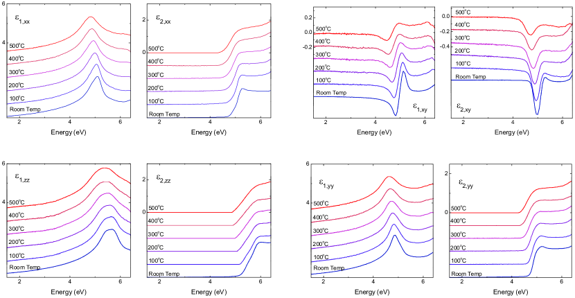
Figure 1 depicts the real and imaginary parts of the dielectric function obtained at temperatures 22∘C, 100∘C, 200∘C, 300∘C, 400∘C, and 500∘C and determined by a wavelength-by-wavelength approach. We observe a distinct broadening accompanied with a pronounced red-shift of the critical point features. To begin with, the below-band-gap squares of the indices of refraction are analyzed, determining for each non-vanishing tensor element. A Cauchy polynomial expansion was used retaining the first three coefficients in the wavelength expansion, augmented by a linear dependence on temperature for the wavelength independent Cauchy coefficient to analyze the wavelength-by-wavelength determined dielectric tensor elements:
| (2) |
where T0 is room temperature. Figure 2 presents the the best-match model parameter result for the wavelength independent portion of Eq. 2, obtained for each temperature investigated (black, boxes), and as a function of temperature (dashed lines). Table 1 lists all below-band-gap model parameters, and compares values reported at room temperature previously (Sturm et al., Ref. Sturm et al., 2015), where we note reasonable agreement except in the shear element .
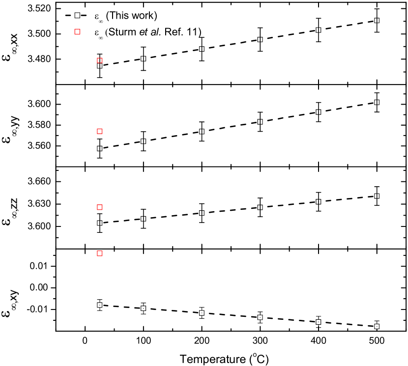
| 3.4(7) | 3.5(6) | 3.6(0) | -0.00(8) | |
| () | (8) | (9) | (8) | -2.(0) |
| () | (5) | (6) | (6) | 0.(4) |
| () | (6) | (4) | -(2) | -(1) |
| 3.7(5)a | 3.2(1)a | 3.7(1)a | -0.0(8)a | |
| 3.479b | 3.574b | 3.626b | 0.016b |
An eigendielectric displacement vector approach as developed by us previouslySchubert et al. (2016) has been utilized to describe electronic transitions and excitonic effects of -Ga2O3 at room temperatureMock et al. (2017). We use this same approach here at elevated temperatures and present model dielectric function parameters in Tab. 2. We find that amplitudes do not change significantly in the temperature range investigated and are therefore not included in the table. We observe that energy parameters decrease with increasing temperature while broadening parameters increase. We note that due to increasing broadening and with the first two transitions polarized along the b-axis so close together, sensitivity to the excitonic binding energy parameter was limited and thus we held it to a constant value of 0.18 eV for CP as determined previously for room temperature.
| CP | CP | CP | CP | CP | CP | |||||||||
|---|---|---|---|---|---|---|---|---|---|---|---|---|---|---|
| Temperature | (deg) | (eV) | (eV) | (eV) | (eV) | (deg) | (eV) | (eV) | (eV) | (eV) | (eV) | (eV) | (eV) | (eV) |
| RoomTemp | 115.1(1) | 4.9(2) | 0.4(0) | 5.0(4) | 0.0(2) | 25.2(1) | 5.1(7) | 0.4(3) | 5.4(0) | 0.0(9) | 5.4(6) | 0.5(4) | 5.6(4) | .01(1) |
| 100∘C | 112.(5) | 4.8(7) | 0.46(6) | 5.0(1) | 0.03(2) | 25.(2) | 5.1(4) | 0.45(0) | 5.3(1) | 0.08(1) | 5.41(7) | 0.5(3) | 5.59(6) | 1.(4) |
| 200∘C | 111.(7) | 4.8(3) | 0.5(2) | 4.9(6) | 0.0(6) | 20.(3) | 5.0(8) | 0.53(8) | 5.2(9) | 0.0(9) | 5.34(9) | 0.6(1) | 5.52(9) | 1.(6)) |
| 300∘C | 111.(7) | 4.7(6) | 0.5(9) | 4.9(2) | 0.0(7) | 20.(1) | 5.0(2) | 0.5(9) | 5.2(2) | 0.1(3) | 5.3(0) | 0.6(8) | 5.4(8) | 2.(0) |
| 400∘C | 110.(4) | 4.6(9) | 0.6(2) | 4.8(5) | 0.0(8) | 19.(8) | 4.9(3) | 0.6(9) | 5.0(9) | 0.(5) | 5.2(8) | 0.8(1) | 5.4(6) | 3.(2) |
| 500∘C | 109.(6) | 4.6(2) | 0.6(7) | 4.7(9) | 0.0(9) | 18.(0) | 4.8(6) | 0.8(0) | 5.1(3) | 0.(7) | 5.2(5) | 0.8(9) | 5.4(3) | 3.1(9) |
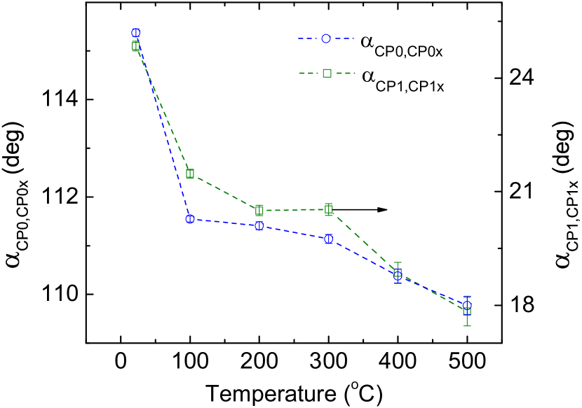
The evolution of the eigendielectric displacement vector direction with temperature is presented in Fig. 3. We observe that in the case of the first two transitions within the a-c plane (CP0 and CP1) along with their excitonic contributions, both of their corresponding eigendielectric displacement vectors orientation angles () decrease. Therefore, we observe that with increasing temperature the direction of the transition corresponding to CP0 (and CP0x) shift closer to the c axis which is at approximately 103.73∘. In much the same way, the direction of the transition corresponding to CP1 (and CP1x) shifts closer to the a axis.
| CP | (eV) | (unitless) | (eV) | (Ref. Sturm et al., 2017)111Parameter average values determined for a-c plane and b axis separately by Sturm et al. | (Ref. Sturm et al., 2017)a |
|---|---|---|---|---|---|
| CP | 4.949222Values approximated from Ref. Sturm et al., 2017 for zero temperature energies. | 9.(5) | 0.0(8) | 10.5 | 0.050 |
| CP | 5.069b | 8.(0) | 0.08(0) | 10.5 | 0.050 |
| CP | 5.18b | 1(3) | 0.1(1) | 10.5 | 0.050 |
| CP | 5.41b | (8) | 0.0(7) | 10.5 | 0.050 |
| CP | 5.52b | 5.(2) | 0.0(3) | 5.5 | 0.025 |
| CP | 5.7b | (5) | 0.0(2) | 5.5 | 0.025 |
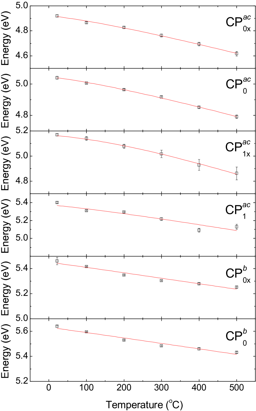
Temperature dependent energy parameters for critical points are shown in Fig. 4. The Bose-Einstein model as described by Viña et al. (Ref. Vina et al., 1984) can be used to describe temperature dependence effects to render the shifts in energy parameters according to
| (3) |
where is the phonon interaction strength and P is the phonon frequency as determined by temperature dependent energy shifts. Recently, Sturm et al. (Ref. Sturm et al., 2017) applied this technique for low temperature generalized ellipsometry analysis of single crystalline -Ga2O3. We also apply this model and extend it to our high temperature measurements.
The resulting lineshapes are shown as red solid lines in Fig. 4 and resulting parameters are given in Tab. 3. We note that in the temperature range investigated, there is limited sensitivity to the parameter , therefore, we have fixed this parameter to a value estimated from results published by Sturm et al. (Ref. Sturm et al., 2017). We find an average isotropic phonon frequency to be approximately 0.65 eV (524.26 cm-1) from all energy parameters for the transitions investigated. The arithmetic average of all (symmetry independent) LPP phonons found by Schubert et al. was found to be 507.5 cm-1 which is in excellent agreement with the value found in the present study.
In summary, we present the dielectric function tensor elements of -Ga2O3 from room temperature up to 500∘C. Further, we provide a description of the linear temperature dependence of the wavelength independent Cauchy coefficient to obtain the temperature effects on the anisotropic below-band-gap monoclinic indices of refraction. Additionally, we determine shifts in eigendielectric vector displacement approach energy parameters due to changes in temperature and model these effects by utilizing a Bose-Einstein lineshape to determine average phonon frequencies. Further, we find a change in the eigendielectric polarization orientation direction with temperature which leads to the possibility that the eigenpolarization directions of the direct band-to-band transitions may be controllable by strain on the crystal lattice or by changes in internal electric fields. This approach could be utilized for design of devices operating at elevated temperatures.
We thank K. Goto and A. Kuramata and the Tamura Corp. for providing the samples studied in this investigation. This work was supported by the National Science Foundation (NSF) through the Center for Nanohybrid Functional Materials (EPS-1004094), the Nebraska Materials Research Science and Engineering Center (DMR-1420645), the Swedish Research Council (VR2013-5580), and the Swedish Foundation for Strategic Research (SSF, FFL12-0181 and RIF14-055). Partial financial support from NSF (CMMI 1337856, EAR 1521428), and J. A. Woollam Foundation is also acknowledged.
References
- Roy et al. (1952) R. Roy, V. G. Hill, and E. F. Osborn, Journal of the American Chemical Society 74, 719 (1952), eprint http://dx.doi.org/10.1021/ja01123a039, URL http://dx.doi.org/10.1021/ja01123a039.
- Tippins (1965) H. H. Tippins, Phys. Rev. 140, A316 (1965), URL http://link.aps.org/doi/10.1103/PhysRev.140.A316.
- Higashiwaki et al. (2012) M. Higashiwaki, K. Sasaki, A. Kuramata, T. Masui, and S. Yamakoshi, Applied Physics Letters 100, 013504 (2012).
- Higashiwaki et al. (2013) M. Higashiwaki, K. Sasaki, T. Kamimura, M. Hoi Wong, D. Krishnamurthy, A. Kuramata, T. Masui, and S. Yamakoshi, Applied Physics Letters 103, 123511 (2013).
- Green et al. (2016) A. J. Green, K. D. Chabak, E. R. Heller, R. C. Fitch, M. Baldini, A. Fiedler, K. Irmscher, G. Wagner, Z. Galazka, S. E. Tetlak, et al., IEEE Electron Device Letters 37, 902 (2016).
- Wong et al. (2016) M. H. Wong, K. Sasaki, A. Kuramata, S. Yamakoshi, and M. Higashiwaki, IEEE Electron Device Letters 37, 212 (2016).
- Yang et al. (2017) J. Yang, S. Ahn, F. Ren, S. Pearton, S. Jang, J. Kim, and A. Kuramata, Applied Physics Letters 110, 192101 (2017).
- Konishi et al. (2017) K. Konishi, K. Goto, H. Murakami, Y. Kumagai, A. Kuramata, S. Yamakoshi, and M. Higashiwaki, Applied Physics Letters 110, 103506 (2017).
- Mock et al. (2017) A. Mock, R. Korlacki, C. Briley, V. Darakchieva, B. Monemar, Y. Kumagai, K. Goto, M. Higashiwaki, and M. Schubert, arXiv preprint arXiv:1704.06711 (In submission Phys Rev. B) (2017).
- Wager (2003) J. F. Wager, Science 300, 1245 (2003), ISSN 0036-8075, eprint http://science.sciencemag.org/content/300/5623/1245.full.pdf, URL http://science.sciencemag.org/content/300/5623/1245.
- Sturm et al. (2015) C. Sturm, J. Furthmüller, F. Bechstedt, R. Schmidt-Grund, and M. Grundmann, APL Materials 3, 106106 (2015).
- Sturm et al. (2016) C. Sturm, R. Schmidt-Grund, C. Kranert, J. Furthmüller, F. Bechstedt, and M. Grundmann, Phys. Rev. B 94, 035148 (2016).
- Furthmüller and Bechstedt (2016) J. Furthmüller and F. Bechstedt, Phys. Rev. B 93, 115204 (2016), URL http://link.aps.org/doi/10.1103/PhysRevB.93.115204.
- Kokubun et al. (2007) Y. Kokubun, K. Miura, F. Endo, and S. Nakagomi, Applied physics letters 90, 031912 (2007).
- Oshima et al. (2008) T. Oshima, T. Okuno, N. Arai, N. Suzuki, S. Ohira, and S. Fujita, Applied physics express 1, 011202 (2008).
- Suzuki et al. (2011) R. Suzuki, S. Nakagomi, and Y. Kokubun, Applied Physics Letters 98, 131114 (2011).
- Schubert et al. (2016) M. Schubert, R. Korlacki, S. Knight, T. Hofmann, S. Schöche, V. Darakchieva, E. Janzén, B. Monemar, D. Gogova, Q.-T. Thieu, et al., Phys. Rev. B 93, 125209 (2016).
- Sturm et al. (2017) C. Sturm, R. Schmidt-Grund, V. Zviagin, and M. Grundmann, Applied Physics Letters 111, 082102 (2017).
- Schubert (2016) M. Schubert, Phys. Rev. Lett. 117, 215502 (2016).
- Aida et al. (2008) H. Aida, K. Nishiguchi, H. Takeda, N. Aota, K. Sunakawa, and Y. Yaguchi, Japanese Journal of Applied Physics 47, 8506 (2008), URL http://stacks.iop.org/1347-4065/47/i=11R/a=8506.
- Sasaki et al. (2013) K. Sasaki, M. Higashiwaki, A. Kuramata, T. Masui, and S. Yamakoshi, Journal of Crystal Growth 378, 591 (2013), ISSN 0022-0248, the 17th International Conference on Molecular Beam Epitaxy, URL http://www.sciencedirect.com/science/article/pii/S0022024813001280.
- Shimamura and Villora (2013) K. Shimamura and E. Villora, Acta Physica Polonica, A 124, 265 (2013).
- Geller (1960) S. Geller, The Journal of Chemical Physics 33, 676 (1960), URL http://scitation.aip.org/content/aip/journal/jcp/33/3/10.1063/1.1731237.
- Vina et al. (1984) L. Vina, S. Logothetidis, and M. Cardona, Physical Review B 30, 1979 (1984).