Robust Optimal Design of Quantum Electronic Devices
Abstract
We consider the optimal design of a sequence of quantum barriers in order to manufacture an electronic device at the nanoscale such that the dependence of its transmission coefficient on the bias voltage is linear. The technique presented here is easily adaptable to other response characteristics. The transmission coefficient is computed using the Wentzel-Kramers-Brillouin (WKB) method, so we can explicitly compute the gradient of the objective function. In contrast with earlier treatments, manufacturing uncertainties are incorporated in the model through random variables and the optimal design problem is formulated in a probabilistic setting. As a measure of robustness, a weighted sum of the expectation and the variance of a least-squares performance metric is considered. Several simulations illustrate the proposed approach.
Keywords: Robust Optimal Design, Nanoelectronics, Stochastic Collocation Methods, WKB Approximation.
1 Introduction
Nanoelectronic devices operate with extremely low intensity currents. Under these circumstances, it
is desirable to have at our disposal mechanisms to produce and control electronic currents with a
high precision. Electronic beams are relatively easy to produce, but their filtering to obtain
nanocurrents with specified properties is much more difficult. A widely used approach consists in
directing the beam on a sequence of quantum barriers with an externally adjustable bias voltage
applied throughout the device. One expects to be able to control the response of the device in the
form of a current whose intensity depends, say, linearly on the applied bias. This setting naturally
leads to an optimal design problem: What must be the width and height of the layers composing the
barriers, supposed fixed in number, in order to achieve this linear response? (Of course, the problem
is quite general, admitting a more complex relation between the external voltage and the current, but
here we deal with the linear case just for simplicity).
There should be no need to stress the importance of the solution to this problem from a practical
point of view, but it must be noticed right from the start that a closed-form, analytic solution is
impossible to obtain in most cases.
The use of numerical computations at some stage is unavoidable, and this
leads to the question of which method to use in order to obtain a good approximation to the solution.
In [9] the non–constant potential energy profile is approximated by piecewise constant potentials. Then, the propagation matrix method [5, 8] is applied to compute the transmission coefficient and, finally, the gradient of a least–squares–type objective function (which is required by the numerical solution method) is computed using the adjoint method. It is important to point out that different discretization processes, which are used to approximate objective functions and/or its gradients, may lead to very different results. Moreover,
it has been observed in some optimization problems [7] that first approximating a cost functional, and then computing the gradient of the approximated one, in general differs from approximating the gradient of the exact cost functional. That is, the schemes ‘first discretize, then optimize’ and ‘first optimize, then discretize’, do not commute in general. Also, as it will be showed later on in this paper, optimizing for the same cost functional via its exact gradient gives different solutions than using an approximate one.
Another issue, which cannot be obviated in a realistic mathematical model, is the presence of uncertainties. There are several sources of uncertainty in the problem under consideration, one of the most important regarding the influence on the computed optimal design being the manufacturing uncertainties. Due to the smallness of the currents involved, and the narrow width of the quantum barriers needed, methods such as MBE (Molecular Beam Epitaxy) or CVD (Chemical Vapor Deposition) are used to growth thin layers (in many cases, monolayers) of some material to build the barriers, two of the preferred ones being and (see [2, 6], for example). These methods allow the growth even of monolayers, but the difficulties inherent to the manufacturing process at a semi–commercial scale lead almost inevitably to inaccuracies that ultimately lead to a potential configuration that may be different from the numerically computed, optimal one [11]. For these reasons, the problem of computing an optimal quantum profile which, in addition, is robust against those uncertainties is an important one. If there is some statistical information about the uncertainties, then the machinery of probability theory gives a framework in which to we can accomodate uncertainties (by using random variables and/or random fields), and model objective functions (by means of expectation and variance operators, among others choices). In [14], this approach has been used for the case in which the cost functional only includes the averaging of a least–squares performance metric, and by using the standard Monte–Carlo method for its numerical resolution.
The present work addresses the problem of the optimal design of a quantum potential profile (modeling a nanoelectronic device) in order to obtain a transmission coefficient linearly depending on an externally applied bias voltage, in the presence of manufacturing uncertainties. The transmission coefficient is explicitly computed by using the WKB method. As a consequence, an explicit formula for the gradient of the cost functional is obtained. A weighted sum of expectation and variance of a random least–squares performance metric is considered as a measure of robustness. The inclusion of the second order statistical moment in the cost functional amounts to a reduction the dispersion of the random transmission coefficient and hence an increase in the robustness of the optimal design. Since the resulting integrand in the cost functional is smooth with respect to a random parameter, a sparse grid stochastic collocation method is used for the numerical approximation of the involved integrals in the random domain. This method preserves the parallelizable character of Monte–Carlo sampling. However, in contrast to Monte–Carlo (which is computationally very expensive, of order , with the number of random sampling points), the stochastic collocation method shows an exponential convergence with respect to the number of sampling points. Several simulations illustrate the proposed approach, which shows itself to be an improvement in accuracy over previous ones of about a .
2 Setting of the Optimal Design Problems
Considered is a nanoscale semiconductor electronic device composed of layers occupying positions . The local potential energy at the th layer is denoted by , . For , the potential energy is denoted by and for it is . It is assumed that a single electron propagating from is incident at and that a voltage bias is applied across the device. A linear approximation of the underlying Poisson’s equation [9, 13] leads to the following expression for the resulting potential energy profile
| (1) |
where is the vector of local layer potentials in the device, and
is the characteristic function of the interval , .
The transmission coefficient of the device is defined as the ratio of current density transmitted from the device at and the incident one at . As explained in detail in [9], may be expressed as
| (2) |
where and , for values of the energy . The cases and may be treated in a similar way. Here is the effective mass of the electron, denotes the electron charge, is Planck’s constant, is the electron energy, and finally solves the following boundary-value problem for the Schrödinger equation
| (3) |
Here denotes the unit imaginary number and the amplitude of the transmitted wave at .
2.1 Deterministic Optimal Design
The (deterministic) optimal design problem considered in this paper is formulated as the following nonlinear data-fitting problem: Given a desired transmission coefficient , which is defined for , and lower, , and upper, , bounds for the local layer potentials, with ,
| (4) |
where is given by (2) with and , .
2.2 Optimal Design Under Manufacturing Uncertainties
As indicated in the introduction, it is very convenient to analyse the robustness of optimal designs with respect to manufacturing uncertainties. These may be modelled by adding a vector of random variables
| (5) |
to the vector of local layer potentials. Here represents a random event and thus is a small unknown error in manufacturing the local potential . Hence, the cost functional considered in problem (4) becomes a random variable given by
| (6) |
In order to obtain a design of the potential energy profile less sensitive with respect to fabrication unknown fluctuations, the new cost functional is considered:
| (7) |
with a weighting parameter. Here and Var denote the expectation and variance operators, respectively. Then, the robust optimization problem is formulated as
| (8) |
where is given by (7).
3 Solving the Optimal Design problems
The numerical resolution of the optimal design problems stated in the preceding section requires the computation of the transmission coefficient (2) and, therefore, the resolution of the boundary-value problem (3). This problem may be numerically approximated by standard numerical methods such as finite differences or finite elements. Another approach is proposed in [9] where, after approximating the potential , as given by (1), by piecewise constant potentials, problem (3) is transformed into a two–dimensional linear non–autonomous difference equation. Here we propose a different approach based on the so–called WKB method [10]. From the point of view of optimization, WKB method is very appealing since, within its range of validity, it provides an explicit form for the solution to (3). From this, explicit expressions for the gradients of the cost functionals considered in problems (4) and (8) are derived. In addition, having an explicit expression for allows us to prove its smoothness with respect to and . From this, both existence of solutions to (4) and (8), as well as designing a computationally very efficient numerical resolution method, will be derived in this section.
We begin by explicitly computing the transmission coefficient (2) and then describe the numerical resolution methods for problems (4) and (8).
3.1 Explicit Computation of Transmission Coefficient
3.1.1 Case of a single potential barrier
For the sake of clarity, consider first the case of a single potential barrier as illustrated in Figure 1.

The WKB method proposes a solution of the Schrödinger equation in the form
| (9) |
with , if for all , and for all .
In the context of quantum electronic devices, solutions to (3) admit a smooth representative in their classes (of regularity class ). Hence, continuity of and its first derivative at the interface point leads to
| (10) |
where
| (11) |
By writing each matrix in (3.1.1) as the product of two matrices as follows
| (12) |
and solving (12) for and ,
| (13) |
Proceeding in the same way at the point , one obtains
| (14) |
where
and
Substituting (14) into (13), we get
| (15) |
Denoting by the product of matrices from to the transmission coefficient (2) takes the form , where is the first entry of . More precisely, the following explicit formula for that transmission coefficient, in the case for all , is obtained:
| (16) |
where is given by (11) and
| (17) |
The case for all is completely analogous. Denoting by
| (18) |
the transmission coefficient is given by
| (19) |
where
| (20) |
3.1.2 Range of validity for WKB method
The condition for the validity of WKB method and therefore for formulas (16) and (19) is that the change in the potential energy over the decay length be smaller than the magnitude of the kinetic energy (see, for instance, [13, p. 483]). For the case , this condition can be expressed as
| (21) |
and for ,
| (22) |
In particular, (21) and (22) constraint the values of and for which the WKB methods applies. Assume that : Since , for all . Hence, by introducing the function
| (23) |
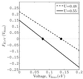
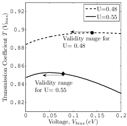
condition (21) is satisfied whenever . Figure 2 displays the functions and its associated transmission coefficient , as given by (16), for and .
 |
 |
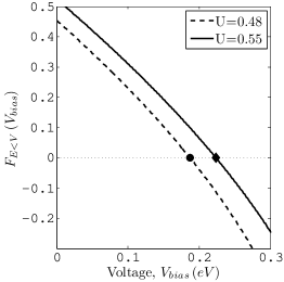
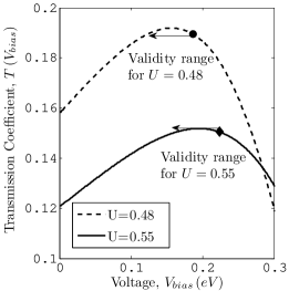
Analogously in the case , by considering the function
| (24) |
condition (22) holds for . Figure 3 plots the functions and the transmission coefficient given in (19 ) for two values of , namely and with the energy of an electron .
 |
 |
3.1.3 Case of multiple potential barriers
Consider now the configuration described at the beginning of Subsection 2.1, which is composed of potential barriers with energy given by (1). Let us denote by
| (25) |
the potential energy of the th barrier and by
| (26) |
The linear relationship between the coefficients of the electron wave function at and the ones at is expressed as
| (27) |
where the form of the transfer matrices depend on the relationship between and . For the cases in which WKB method may be applied, has been computed in the preceding section. For the spatial regions for which WKB method does not apply, appropriate connection formulae must be used. For instance, as in [8, 14], the linear potential is approximated by piece-wise contant potential for which explicit expressions of are well-known [5].
Finally, as in the case of a single potential barrier, the transmission coefficient is obtained from (27).
3.2 Numerical Resolution Method
Before describing the numerical methods proposed in this paper for solving (4) and (8), let us briefly consider the question concerning the existence of solution for such problems.
From the explicit expressions (16) and (19), and taking into the computations in Subsection 3.1.3, it is clear that the functionals and , which have been considered in problems (4) and (8), respectively, are smooth (of regularity class ). In addition, the set of admissible designs is a compact set of . As a consequence, the following existence result holds.
The nonlinear mathematical programming problem (4) is standard and may be solved by several methods, typically by a gradient-based method. In this paper, a subspace trust region method, which is based on the interior-reflective Newton method, as proposed in [3, 4], is used. This algorithm is implemented in the MatLab constrained optimization routine fmincon.
More challenging is the robust optimal design problem (8). The brute–force sampling Monte Carlo is the most commonly method used to solve this kind of problems. However, for smooth (with respect to the random parameter) functions, sparse grid, stochastic collocation methods are able to keep the same accuracy as Monte Carlo and, in addition, are computationally much more efficient [1]. In our case, again from (16) and (19) it is not hard to show that , as defined in (6), is analytic with respect to the random variable . For this reason, we propose an adaptive, isotropic, sparse grid, stochastic collocation method to approximate both, the cost functional and its gradient. Then, the robust optimal design problem (8) can be solved as in the deterministic case.
In order to explain the method for approximating integrals in the random domain used in this paper, let us first introduce some notation. By we denote a complete probability space. is the set of outcomes, is the -algebra of events and is a probability measure. , , are the images spaces of the sample space through the real-valued random variables considered in (5), and is the product space. Assuming that the distribution measure of is absolutely continuous with respect to the Lebesgue measure, there exists a joint probability density function for . Hence, is mapped to , where is the -algebra of Borel sets on , and is the Lebesgue measure. Finally, the expectation and variance of take the form
| (28) |
| (29) |
Following [1, 12], the isotropic sparse grid of sampling quadrature nodes is defined as follows. Starting from an integer (called the level), the index set
is considered, with . The level determines the number of collocation points in the th stochastic direction, which for the case of Smolyak rule is given by
Smolyak quadrature rule applied to a generic function gives
| (30) |
where , with , is a quadrature rule in which the coordinates of the nodes are the same as those for the 1D quadrature formula and its associated weights are the difference between those for the and levels.
It remains to analyze the question on how to properly choose the quadrature level . For this:
-
(1)
A positive, large enough, integer , and a tolerance level are fixed.
-
(2)
The first and second order statistical moments of , as given by (28) and the first term in the right-hand side of (29), are approximated by using (30), with level . These two approximations, which are denoted by and , respectively, play the role of enriched or reference values for the exact values of the first two statistical moments of , which, obviously, cannot be explicitly computed.
-
(3)
Finally, the level is linearly increased from to until the stopping criterion
(31) is satisfied. Here and denote, respectively, approximations, by using (30) with level , of the first two statistical moments of . If (31) is not satisfied for the tolerance and the initial , then the reference level is increased.
For more details on this adaptive algorithm, including its convergence, we refer the reader to [1] and the references therein.
4 Numerical Simulations
In this section, numerical results for problems (4) and (8) are presented and discussed. In all experiments, a four layers device is considered of the same thickness (nm), so that the total length is nm. The desired linear transmission coefficient is
| (32) |
Quadratic and square root transmission coefficients may be treated analogously. The design is based on equally spaced bias voltages. Hence, , . The electron mass is , with Kg (which is appropriate for an electron in the conduction band of ), its energy is eV, and its charge C. Planck’s constant is . The lower and upper bounds for the design variable are taken as eV and eV, respectively.
The goal of this section is twofold: On the one hand, it is aimed at analyzing the differences that may occur when using exact gradients or numerical gradients in the optimization algorithm. On the other hand, we want to analyze the influence of manufacturing uncertainties on the computed designs. We deal with these issues in the following subsections.
4.1 Exact versus numerical gradient
In this experiment, the deterministic problem (4) is solved, by using the MatLab routine fmincon, in the cases where: (a) The exact gradient is provided, as computed from the explicit expression for the cost functional in Section 3, and (b) the gradient is numerically computed by using finite differences. In both cases, the algorithm is initiated with eV, , and the stopping criterion, provided by the MatLab routine fmincon, is fixed to .
First column in Table 1 displays results for the values of the cost functional after convergence of the algorithm. The optimal energy potentials are showed in the remaining columns. Inspection of Table 1 reveals (as expected) that performance increases by using the exact gradient. Precisely, the value of the objective function obtained by using the optimal design as computed with the exact gradient improves in about the corresponding one obtained via the numerical gradient.
| Gradient | |||||
|---|---|---|---|---|---|
| Exact | |||||
| Numerical |
4.2 Deterministic design versus design under uncertainty
Manufacturing uncertainties are modelled by random variables uniformly distributed in , i.e., for all . As an illustration, the cases and are considered. As in the preceding example, the algorithm is initiated with eV, , and the stopping criterion is fixed to .
Case 1: , which represents of error in manufacturing each one of the potentials .
The algorithm described in Subsection 3.2 has been implemented by using the Sparse Grids Matlab kit 15.8 (see http://csqi.epfl.ch and [1]). The stopping criterion (31), with , is satisfied for and , which corresponds to collocation nodes in the random domain Figure 4 displays the rates of convergence of the isotropic sparse grid algorithm.

Table 2 shows the results, after convergence of the algorithm, for the expectation and the standard deviation of the cost functional given by (6). As expected, the optimal design in mean () provides a solution which reduces the impact of manufacturing errors in comparison with the deterministic approach (see first and second rows in the first column of Table 2). It is also observed that increasing the value of the weighing parameter reduces the dispersion of the computed designs. These results are more significant when the level of uncertainty increases, as pointed out in Table 3.
| Design | ||||||
|---|---|---|---|---|---|---|
| Deterministic | ||||||
Case 2: , which corresponds to of noise. The same procedure as in the preceding case has been applied. in this case, (31) is satisfied, with , for and , which corresponds to collocation nodes.
| Design | ||||||
|---|---|---|---|---|---|---|
| Deterministic | ||||||
The same qualitative results as in the preceding case are observed in Table 3. However, since in this case the level of manufacturing uncertainties is higher, the differences of corresponding solutions are much more significant than in the preceding case. Indeed, for of noise, the reduction in the mean value of for the mean optimal value (), in comparison with the deterministic optimal design, is of the order of . For the case of of noise, this reduction is of the order of . The decreasing if the standard deviation of the computed designs is also much more significant in the current case than in the case of of manufacturing noise.
5 Conclusions
We have addressed the problem of determining optimal designs of nanoelectronic devices whose physical behavior is governed by the time–independent Schrödinger equation. Two situations are considered: A deterministic version of the problem, and the more realistic case where manufacturing uncertainties are accounted for. In both cases, the corresponding optimal design problems are formulated as the minimization of a least–squares performance metric. In the stochastic case, the variance of the random metric is incorporated in the cost functional as a measure of robustness. An explicit expression for that metric is computed using a semi–classical approximation. Having at our disposal an analytic expression for the cost functional has the following advantages:
-
(a)
At the theoretical level, it is easily deduced that the cost functional is smooth (of regularity class ) with respect to the design variables. As a consequence, the existence of solutions for both optimization problems is proved.
-
(b)
In the deterministic case, an explicit expression for the gradient of the cost functional is obtained. Numerical simulations in Subsection 4.1 show the relevance of this issue, at least in the specific problem considered in this work, when gradient–based minimization algorithms are used as the numerical resolution method.
-
(c)
In the stochastic optimization problem, it is also deduced that integrands, which appear in the considered cost functional, are analytic with respect to the random vector parameter. Thus, stochastic collocation methods (which possess an exponential rate convergence with respect to the number of sampling points and are, computationally, much more efficient than the classical brute-force Monte-Carlo method) are preferred.
The results obtained show an improvement of the accuracy in the linear response characteristic of about over previous, brute–force, approaches. Moreover, the robustness of the design is manifest even under weight values of in the variance (physically, as seen in in Table 2, this would amount to pass from a design using Germanium, with a band gap of 0.7eV, to one using Silicon, whose band gap is 1.1eV, so that extreme case is still physically feasible).
As noticed along the paper, the semi–classical approach used in this work has the drawback that constraints the values of the applied bias voltage and those of the local energy potentials. Accordingly, the whole range of possible energies and potential profiles may be covered by using the approach proposed in this work in combination with appropriate connection formulas, for instance, the ones presented in [9].
Acknowledgements. OM was supported by grant number from CONACyT (Consejo Nacional de Ciencia y Tecnología, Mexico), under program Movilidad en el extranjero (291062). FP was supported by projects DPI2016-77538-R from Ministerio de Economía y Competitividad (Spain) and 19274/PI/14 from Fundación Séneca (Agencia de Ciencia y Tecnología de la Región de Murcia (Spain)). JAV was supported by a CONACyT project CB-179115.
References
- [1] J. Bäck, F. Nobile, L. Tamellini and R. Tempone: Stochastic spectral Galerkin and collocation methods for PDEs with random coefficients: a numerical comparison. In ‘Spectral and High Order Methods for Partial Differential Equations’. Lecture Notes in Computational Science and Engineering. Vol 76, 43–66. Springer, 2011.
- [2] C. Bergeron et al.: Chemical vapor deposition of monolayer directly on ultrathin for low-power electronics, Appl. Phys. Lett. 110 (2017) 053101.
- [3] T. F. Coleman, Y. Li: On the convergence of reflective Newton methods for large-scale nonlinear minimization subject to bounds, Mathematical Programming 67 (2) (1994) 189–224.
- [4] T. F. Coleman, Y. Li: An interior, thrust region approach for nonlinear minimization subject to bounds, SIAM J. Optimization 6 (1996) 418–445.
- [5] R. Gilmore: Elementary Quantum Mechanics in One Dimension, The Johns Hopkins University Press, 2004.
- [6] C. Gong et al.: Metal Contacts on Physical Vapor Deposited Monolayer , ACS Nano 7 (12) (2013) 11350–11357.
- [7] W. W. Hager, Runge-Kutta methods in optimal control and the transformed adjoint system, Numer. Math., 87, 247-282 (2000).
- [8] A. F. J. Levi, Applied Quantum Mechanics, Cambridge University Press, Cambridge, UK, 2006.
- [9] A. F. J. Levi and I. G. Rosen, A novel formulation of the adjoint method in the optimal design of quantum electronic devices, SIAM J. Control Optim. 43(5), 3191-3223 (2010).
- [10] V. P. Maslov and M. V. Fedoriuk, Semi-Classical Approximation in Quantum Mechanics, D. Reidel Publishing Company, 1981.
- [11] P. Schmidt, S. Haas and A. F. J. Levi, Synthesis of electron transmission in nanoscale semiconductor devices, Applied Physics Letters 88, 013502 (2006).
- [12] S. Smolyak, Quadrature and interpolation formulas for tensor products of certain classes of functions, Doklady Akademii Nauk SSSR, 4, 240-243 (1963).
- [13] S. Wang, Fundamentals of Semiconductor Theory and Device Physics, Prentice-Hall, Englewood Cliffs, N.J., 1989.
- [14] J. Zhang and R. Kosut, Robust design of quantum potential profile for electron transmission in semiconductor nanodevices, Proceedings of the European Control Conference, Kos, Greece, 2007.