Charge doping and large lattice expansion in oxygen-deficient heteroepitaxial \ceWO3
Abstract
Tungsten trioxide is a versatile material with widespread applications ranging from electrochromic and optoelectronic devices to water splitting and catalysis of chemical reactions. For technological applications, thin films of \ceWO3 are particularly appealing, taking advantage from high surface-to-volume ratio and tunable physical properties. However, the growth of stoichiometric, crystalline thin films is challenging because the deposition conditions are very sensitive to the formation of oxygen vacancies. In this work, we show how background oxygen pressure during pulsed laser deposition can be used to tune the structural and electronic properties of \ceWO3 thin films. By performing X-ray diffraction and low-temperature transport measurements, we find changes in \ceWO3 lattice volume up to , concomitantly with an insulator-to-metal transition as a function of increased level of electron doping. We use advanced ab initio calculations to describe in detail the properties of the oxygen vacancy defect states, and their evolution in terms of excess charge concentration. Our results depict an intriguing scenario where structural, electronic, optical, and transport properties of \ceWO3 single-crystal thin films can all be purposely tuned by a suited control of oxygen vacancies formation during growth.
IIntroduction
The tungsten oxide \ceWO3 holds a special place in the family of complex oxides, since its perovskite \ceABO3 crystal structure has an empty \ceA-site. This characteristic determines an open crystalline structure, which is prone to host interstitial species which act as dopants for the otherwise insulating material Granqvist (2000); Hirai et al. (2011); Haldolaarachchige et al. (2014); Soma et al. (2016); Hamdi et al. (2016). For these reasons \ceWO3 finds wide use in electrochromic, optoelectronic and gas sensing applications Deb (2008); Long et al. (2015); Cong et al. (2016). Most works so far focused on thick films, amorphous layers and nanorods LeGore et al. (1997); Tägtström and Jansson (1999). Only recently the growth of crystalline thin films has been demonstrated by means of several techniques such as sputtering, molecular beam epitaxy and pulsed laser deposition Du et al. (2014); Leng et al. (2015); Kalhori et al. (2016); Herklotz et al. (2017). Because \ceWO3 structure and electronic properties are very sensitive to oxygen stoichiometry Sahle and Nygren (1983); He et al. (2013); Meng et al. (2015); Altendorf et al. (2016), a precise control of oxygen partial pressure during the growth process is crucial to obtain high quality thin films.
In this work, we study the effects of oxygen pressure during pulsed laser deposition of \ceWO3 thin films, and show how it modifies the material structural and electronic properties. X-ray diffraction measurements reveal that heteroepitaxial \ceWO3 thin films are in a tetragonal phase, where the out-of-plane lattice parameter can be gradually tuned up to , changing from measured in the most stoichiometric compound to in the most oxygen deficient case. By performing transport measurement, we find a semiconducting trend characterised by an activated transport regime, with an energy gap that vanishes for increased level of oxygen vacancies. These findings are corroborated by ab initio calculations, showing that oxygen vacancies form in-gap states, effectively donating electron carriers and increasing \ceWO3 lattice volume. Our results show how to obtain \ceWO3 thin films with high crystal quality and controlled electronic properties.


IIFilm growth
To study the effect of background oxygen pressure () on \ceWO3 thin films grown by pulsed laser deposition (PLD), we prepare a series of samples deposited on top of \ceTiO2-terminated \ceSrTiO3 (001) substrates. We use a laser fluence of , a repetition rate of , a target-to-sample distance of and a fixed deposition duration of 1000 laser pulses. The growth temperature is , while is varied in the range . The plasma plume appears more diffused at lower and more intense at higher (Fig. S1). This is because the oxygen pressure in the PLD chamber strongly influences the plume dynamics, enhancing scattering of the ablated species and thermalisation with the background gas. As a consequence, their oxidation state and kinetic energy can be modified, so that the stoichiometry of the deposited material strongly depends upon Wicklein et al. (2012); Groenendijk et al. (2016). We monitor the growth in situ by reflection high-energy electron diffraction (RHEED) and observe clear intensity oscillations (Fig. 1a) when is between . The RHEED pattern evolves from three well defined diffraction points, typical for \ceSrTiO3 single crystals Haeni et al. (2000), to a series of stripes that indicate bidimensional film growth. As shown in the photograph of Fig. 1b, the sample colour is also affected by the oxygen pressure, and it gradually changes from transparent to dark grey with lowering . All the deposited \ceWO3 films have a step-and-terrace surface morphology with single unit cell steps (Figs. 1c and 1d). This structure mimics the underlying \ceSrTiO3 substrate, indicating uniform growth (Fig. S2). The samples have very low surface roughness (Fig. 1e) ranging from , which is comparable to what we measure in a pristine substrate (). Interestingly, the roughness is minimal at , pressure for which the RHEED oscillations during growth are more accentuated. This characterisation indicates that for all in the explored range the films grow with a smooth surface morphology.
IIIExperimental characterisation
III.1X-ray diffraction
To evaluate the crystal quality of our \ceWO3 thin films, we perform X-ray diffraction measurements. Figure 2a shows – scans around the sharp (001) and (002) peaks of the \ceSrTiO3 substrate. The \ceWO3 film grown at presents peaks at and , surrounded by neat finite size oscillations that demonstrate a high crystalline quality. No additional diffraction peaks are observed, indicating that the thin films are in a single crystal phase. For lower , the peaks and finite size oscillations gradually shift to lower angles. At the finite size oscillations become less defined, concurrently with a broadening of the diffraction peaks. Such signal degradation is usually determined by a decreased crystal quality, similarly to what has previously been observed for highly doped \ceWO3 He et al. (2016); Wang et al. (2016). We evaluate the presence of defects in \ceWO3 by measuring rocking curves around the film (001) peak. In Fig. 2b we find for all samples a sharp peak with full width at half maximum between and , very close to the value found for the underlying \ceSrTiO3 substrate (). The sharp rocking curves indicate that the \ceWO3 films have low mosaicity and present single crystal quality. Performing reciprocal space maps (Fig. S3) we find that the in-plane lattice of all films is coherently strained to the substrate one (). By using Bragg’s law, we extract in Fig. 2c the out of plane -axis parameter from the position of \ceWO3 diffraction peaks. At we obtain . Samples grown at lower present a larger -axis parameter (Fig. 2c). Because all films are epitaxially locked in-plane to the substrate lattice, this points to an increased \ceWO3 unit cell volume, a trend compatible with a higher concentration of oxygen vacancies, as previously reported for oxygen deficient thin films grown by PLD McIntosh et al. (2006); Choi et al. (2008); Hauser et al. (2015); Lorenz et al. (2016); Enriquez et al. (2017). For the c-axis becomes bigger than , signalling a transition from tensile to compressive strain. We note that, concomitantly with this crossover, the finite size oscillations disappear, suggesting that films grown at have a lower crystal quality.
By simulating the finite size fringes of the XRD data with a kinematic scattering model, we extract in Fig. 2d the number of unit cells forming the thin films. We find a constant for , and lower values at higher oxygen pressures. Considering that all films were deposited with the same total number of laser pulses, we associate the decreased with enhanced scattering of the plasma plume at higher pressures, which reduces the amount of material deposited on the substrate. For , the absence of finite size oscillations makes impossible to determine the number of unit cells by – measurements. We thus perform X-ray reflectivity measurements (raw data in Fig. S4) from which we extract the thin film thickness and interface roughness indicated by the crosses in Figs. 2e and 2f. The total film thickness shows an increasing trend with lower pressure, which is a combined effect of the -axis expansion and decreased plume scattering. In Fig. 2e we also evaluate the film thickness from the – measurements as (circles) and find good agreement with the reflectivity data. Concerning the interface roughness in Fig. 2f, we find a minimum at , consistent with the minimum value obtained from the topography data of Fig. 1e. These measurements show that \ceWO3 -axis parameter can be changed up to by tuning the oxygen pressure during growth, while preserving the in-plane match with the substrate lattice and a flat surface. It is then interesting to study how the film electronic properties are affected by , which we investigate by low-temperature transport measurements.
III.2Electrical transport

To investigate the effect of oxygen vacancies on \ceWO3 electronic properties, we measure resistivity versus temperature curves on samples grown in different oxygen pressure conditions. The measurements are performed in a van der Pauw configuration, and electrical contact to \ceWO3 is obtained with ultrasonic bonded Al wires. All the samples show a semiconducting behaviour (Fig. 3a), with the resistivity monotonously increasing upon lowering temperature. The resistivity is calculated using the film thickness measured by X-ray reflectivity. Lower results in flatter curves with lower room-temperature resistivity, as highlighted in Fig. 3b where we report for the different samples. The data shows a sigmoid trend, with a variation of more than 5 orders of magnitude in the studied range. Such trend is comparable to the one observed for the -axis parameter in Fig. 2c, suggesting the existence of a direct correlation between the lattice expansion and the electronic doping. We describe the transport data using an Arrhenius-type behaviour
| (1) |
where is the activation energy for charge transport. The experimental curves are fit from room temperature down to (dashed lines in Fig. 3a), showing good agreement (fits on a larger temperature range are discussed in Fig. S5). We extract at the highest , which is about one order of magnitude smaller than the optical band of found in bulk \ceWO3 Bullett (1983); Sahle and Nygren (1983). This suggests that the observed activated transport arises from localized states lying inside \ceWO3 band gap, which formed in a certain amount even at the highest value. At lower , the concentration of oxygen vacancies in the film increases determining a vanishing . Even though the \ceWO3 films are on the verge of an insulator-to-metal transition, we measure semiconducting behaviour even at the highest vacancies concentration. This is different from what observed with other doping mechanism, where a metallic state was achieved at high doping levels Sahle and Nygren (1983); Haldolaarachchige et al. (2014); Altendorf et al. (2016); Yoshimatsu et al. (2016). Decreased crystal quality and disorder during low-pressure PLD growth are the most probable causes for the persistent semiconducting state measured in our most doped \ceWO3 thin films.
To get indication on the density of the charge carriers, we perform low temperature magnetotransport measurements. Because most of the samples are highly resistive, reliable Hall measurements could be obtained only for samples grown at . In this high-doping conditions, all the samples show similar magnetotransport data (Fig. S6), from which we extract a carrier density and a mobility at , in agreement with previous reports of oxygen-deficient \ceWO3 materials Meng et al. (2015); Altendorf et al. (2016). The measured electron density corresponds to about electrons per unit cell, which would be equivalent to an oxygen vacancy concentration of about , if these are the only source of electron donors.
IVAb initio calculations

| Bulk -\ceWO3 | \ceWO3 | \ceWO_2.94 | \ceWO_2.88 | |
|---|---|---|---|---|
| \ceO vac. | ||||
| () | 3.75 | 3.685 | 3.72 | 3.73 |
| () | 2.71 | 2.83 | - | - |
| () | 0.56 | 0.85 | 2.41 | 1.16 |
To investigate the origin of the observed structural and transport behaviour of \ceWO3 films, we performed ab initio calculations by variational pseudo-self-interaction-corrected (VPSIC) density functional theory (DFT) Filippetti et al. (2011); Archer et al. (2011); Puggioni et al. (2012); Delugas et al. (2013a). To validate our results, we first calculated several \ceWO3 bulk phases (further details in Fig. S7 and the Supplemental Material). The growth on \ceSrTiO3 substrates was simulated using pseudo-cubic supercells, with in-plane lattice constant fixed at and the orthogonal axis left free to relax. The calculations show that the stress associated with the planar expansion is partially relieved with a shrinkage of the out-of-plane lattice parameter to (Table 1). This value is comparable with the experimental data of \ceWO3 films grown at the highest oxygen pressure reported in Fig. 2c, which are thus identified as stoichiometric.
Starting from the strained \ceWO3 structure, we introduce vacancies by removing oxygen atoms in the \ceWO2 crystal planes. We study oxygen vacancy concentrations of (\ceWO_2.94) and (\ceWO_2.88). After a further structural relaxation, our calculations find a lattice increase to and for the two vacancy concentrations. This expansion is in qualitative agreement with our experimental results of Fig. 2, even though the calculated values are considerably lower than what measured for films grown at low pressure. Previous literature reports show that the lattice expansion due to oxygen vacancies is maximum when the charge is fully localised Marrocchelli et al. (2012, 2013). As discussed in the following, the structures described by our DFT calculations are in the metallic regime, and this may partially explain the quantitative discrepancy with the experiments. Furthermore, temperature-related effects, which are not included in our calculations, could also affect the lattice expansion Glensk et al. (2014).
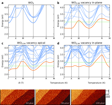
In Fig. 4a we show the calculated in-plane band structure for strained \ceWO3 films with different oxygen vacancy concentrations (extended plots in Fig. S8). A single oxygen vacancy generates an excess of two electrons. In the limit of an isolated point defect, this charge remains trapped by the \ceW atoms surrounding the vacancy, which change their ionic charge from the stoichiometric \ceW^6+ to a lower value, which also gives rise to colour centres responsible for the photochromic effect Bange (1999); Deb (2008). Localisation may eventually be strengthened by the formation of small polarons Bange (1999). According to our calculations, the excess charge reverses into the \cet_2g orbitals of the \ceW atoms, forming a shallow band right below the bottom of the conduction band (orange band in Fig. 4a). Although this band is optically separated from the bulk-like \cet_2g conduction bands running above it, the system for both the examined doping levels is metallic, as indicated by the position of the Fermi energy (green dashed lines in Fig. 4a). The defect state can be visualised in real space through the isosurface plot of Fig. 4b: the defect charge is mostly localised on the two W atoms nearest neighbours of the vacancy, with clear \cet_2g symmetry. This is also seen by the broader bandwidth of the vacancy state along the diagonal direction \ceX-M, characteristic of \cet_2g orbitals, instead of the cubic edge direction \ceΓ-X.
In Table 1 we report the band gaps and effective masses along the planar \ceΓ-M direction. The vacancy-free structure shows an insulating state with a direct gap at the \ceΓ point, substantially larger than the indirect gap in bulk -\ceWO3 of . This is a consequence of the tensile strain present in the structure which stretches the planar bonds and reduces the \cet_2g bandwidth, as evidenced by the increased effective mass. Even though the \ceWO_2.94 and \ceWO_2.88 structures have a small optical gap at of and , respectively, they show metallic character in transport due to the broader density of states in the orthogonal direction (Fig. S8). With more excess charge the gaps and effective masses are progressively reduced, due to electronic correlation and band filling effects, which cause a spread in the bandwidth with respect to the empty conduction bands of the undoped system. For lower vacancy concentration, up to the limit of isolated point defect, instead, the carrier density is expected to be reduced, leading to the formation of an insulating state.
In order to theoretically estimate electron mobility and resistivity in a wider range of vacancy concentrations, we apply the Bloch-Boltzmann approach to mix the ab initio band energies of the \ceWO_2.94 structure with a model description of the electron–phonon scattering Filippetti et al. (2012); Delugas et al. (2013b). We tune the Fermi level in a rigid band approximation to simulate the variation in the excess carrier density produced by the vacancies. Results of three-dimensional averages of mobility versus carrier density at are reported in Fig. 4c. As a consequence of the increasing population of high-energy \cet_2g bands of \ceWO3, the mobility increases with the carrier density and, for vacancies, we find and (white circle in Fig. 4c). In our oxygen deficient films, we measure a Hall mobility (orange diamond in Fig. 4c and raw data in Fig. S6) which, in our calculations, would be achieved for a considerably lower carrier density . By using the ab initio transport coefficients, we calculate the corresponding resistivity versus temperature in Fig. 4d. At densities below we observe an insulating transport regime, for which only the energy-flat, lowest portion of the defect state is populated, with vanishing band velocities. In this regime, the electrical transport is thermally activated, similarly to what we measure experimentally. Above , an insulator-to-metal transition is observed in our calculations, but it is not achieved experimentally. This is a clear indication that disorder in our thin films plays a crucial role in preventing occurrence of an insulator-to-metal transition, consistently with the experimental observation of a low electron mobility.
Several aspects of transport calculations are in good agreement with the measurements. In particular, the amplitude of resistivity versus temperature matches well the experimental data, and the shallow temperature dependence of the resistivity is experimentally verified for most of the doped samples. Furthermore, the calculations show that an insulator-to-metal transition occurs for , a value consistent with our experimental observations. On the other hand, there is an offset between calculated and Hall charge densities corresponding to the same mobility value, the former being two orders of magnitude lower. This discrepancy suggests that a large portion of excess charge in the samples may be scarcely mobile, possibly stuck in deep traps or in highly localized polarons. The hypothesis of additional charge in the samples coming from in-gap states is coherent with the experimentally measured Arrhenius trend of the resistivity.
VConclusions
In summary, we demonstrated that structural, electronic and transport properties of \ceWO3 thin films can be controlled by changing the oxygen pressure during PLD growth. The out-of-plane lattice constant of our thin films increases up to as a consequence of the introduction of oxygen defects, while a pseudocubic phase of single crystal quality is maintained. Oxygen vacancies act as electron donors and dope the material towards a metallic state. Our VPSIC-DFT calculations describe oxygen vacancies in strained \ceWO3 films as a weakly localized, shallow donors of \cet_2g orbital character, lying only a few tents of below the bulk-like \cet_2g mobility edge. According to our Bloch-Boltzmann rigid-band calculations, full localization is only reached for , corresponding to an extremely small vacancy concentration. While several aspects of the calculations are coherent with the measurements, it is very likely that additional effects, like disorder and defect clusterization, can enhance charge localization, thus shifting to higher values the vacancy concentration threshold which separate charge-localized and delocalized regime. Our results represent a fundamental step towards the understanding and engineering of a material which is likely destined to become a rising star in the energy and nanoelectronic applications of the future.
VIAcknowledgments
This work was supported by The Netherlands Organisation for Scientific Research (NWO/OCW) as part of the Frontiers of Nanoscience program (NanoFront) and by the Dutch Foundation for Fundamental Research on Matter (FOM). The research leading to these results has received funding from the European Research Council under the European Union’s H2020 programme/ ERC GrantAgreement n. [677458].
References
- Granqvist (2000) C. G. Granqvist, Solar Energy Materials and Solar Cells 60, 201 (2000).
- Hirai et al. (2011) D. Hirai, E. Climent-Pascual, and R. J. Cava, Physical Review B 84, 174519 (2011).
- Haldolaarachchige et al. (2014) N. Haldolaarachchige, Q. Gibson, J. Krizan, and R. J. Cava, Physical Review B 89, 104520 (2014).
- Soma et al. (2016) T. Soma, K. Yoshimatsu, and A. Ohtomo, Applied Physics Express 9, 075801 (2016).
- Hamdi et al. (2016) H. Hamdi, E. K. Salje, P. Ghosez, and E. Bousquet, Physical Review B 94, 245124 (2016).
- Deb (2008) S. K. Deb, Solar Energy Materials and Solar Cells 92, 245 (2008).
- Long et al. (2015) H. Long, W. Zeng, and H. Zhang, Journal of Materials Science: Materials in Electronics 26, 4698 (2015).
- Cong et al. (2016) S. Cong, F. Geng, and Z. Zhao, Advanced Materials 28, 10518 (2016).
- LeGore et al. (1997) L. J. LeGore, O. D. Greenwood, J. W. Paulus, D. J. Frankel, and R. J. Lad, Journal of Vacuum Science & Technology A: Vacuum, Surfaces, and Films 15, 1223 (1997).
- Tägtström and Jansson (1999) P. Tägtström and U. Jansson, Thin Solid Films 352, 107 (1999).
- Du et al. (2014) Y. Du, M. Gu, T. Varga, C. Wang, M. E. Bowden, and S. A. Chambers, ACS Applied Materials & Interfaces 6, 14253 (2014).
- Leng et al. (2015) X. Leng, J. Pereiro, J. Strle, A. T. Bollinger, and I. Božović, APL Materials 3, 096102 (2015).
- Kalhori et al. (2016) H. Kalhori, S. B. Porter, A. S. Esmaeily, M. Coey, M. Ranjbar, and H. Salamati, Applied Surface Science 390, 43 (2016).
- Herklotz et al. (2017) A. Herklotz, S. F. Rus, S. Kc, V. R. Cooper, A. Huon, E.-J. Guo, and T. Z. Ward, APL Materials 5, 066106 (2017).
- Sahle and Nygren (1983) W. Sahle and M. Nygren, Journal of Solid State Chemistry 48, 154 (1983).
- He et al. (2013) X. He, Y. Yin, J. Guo, H. Yuan, Y. Peng, Y. Zhou, D. Zhao, K. Hai, W. Zhou, and D. Tang, Nanoscale Research Letters 8, 50 (2013).
- Meng et al. (2015) X. Meng, F. Quenneville, F. Venne, E. Di Mauro, D. Işık, M. Barbosa, Y. Drolet, M. M. Natile, D. Rochefort, F. Soavi, et al., The Journal of Physical Chemistry C 119, 21732 (2015).
- Altendorf et al. (2016) S. G. Altendorf, J. Jeong, D. Passarello, N. B. Aetukuri, M. G. Samant, and S. S. Parkin, Advanced Materials 28, 5284 (2016).
- Wicklein et al. (2012) S. Wicklein, A. Sambri, S. Amoruso, X. Wang, R. Bruzzese, A. Koehl, and R. Dittmann, Applied Physics Letters 101, 131601 (2012).
- Groenendijk et al. (2016) D. J. Groenendijk, N. Manca, G. Mattoni, L. Kootstra, S. Gariglio, Y. Huang, E. van Heumen, and A. D. Caviglia, Applied Physics Letters 109, 041906 (2016).
- Haeni et al. (2000) J. H. Haeni, C. D. Theis, and D. G. Schlom, Journal of Electroceramics 4, 385 (2000).
- He et al. (2016) Y. He, M. Gu, H. Xiao, L. Luo, Y. Shao, F. Gao, Y. Du, S. X. Mao, and C. Wang, Angewandte Chemie International Edition 55, 6244 (2016).
- Wang et al. (2016) Z. Wang, Y. He, M. Gu, Y. Du, S. X. Mao, and C. Wang, ACS Applied Materials & Interfaces 8, 24567 (2016).
- McIntosh et al. (2006) S. McIntosh, J. F. Vente, W. G. Haije, D. H. Blank, and H. J. Bouwmeester, Chemistry of Materials 18, 2187 (2006).
- Choi et al. (2008) E. Choi, J. Kim, D. Cuong, and J. Lee, in 17th IEEE International Symposium on the Applications of Ferroelectrics, 2008, Vol. 1 (IEEE, 2008) pp. 1–2.
- Hauser et al. (2015) A. J. Hauser, E. Mikheev, N. E. Moreno, J. Hwang, J. Y. Zhang, and S. Stemmer, Applied Physics Letters 106, 092104 (2015).
- Lorenz et al. (2016) M. Lorenz, G. Wagner, V. Lazenka, P. Schwinkendorf, M. Bonholzer, M. J. Van Bael, A. Vantomme, K. Temst, O. Oeckler, and M. Grundmann, Materials 9, 44 (2016).
- Enriquez et al. (2017) E. Enriquez, A. Chen, Z. Harrell, P. Dowden, N. Koskelo, J. Roback, M. Janoschek, C. Chen, and Q. Jia, Scientific Reports 7 (2017).
- Bullett (1983) D. W. Bullett, Journal of Physics C: Solid State Physics 16, 2197 (1983).
- Yoshimatsu et al. (2016) K. Yoshimatsu, T. Soma, and A. Ohtomo, Applied Physics Express 9, 075802 (2016).
- Filippetti et al. (2011) A. Filippetti, C. D. Pemmaraju, S. Sanvito, P. Delugas, D. Puggioni, and V. Fiorentini, Physical Review B 84, 195127 (2011).
- Archer et al. (2011) T. Archer, C. D. Pemmaraju, S. Sanvito, C. Franchini, J. He, A. Filippetti, P. Delugas, D. Puggioni, V. Fiorentini, R. Tiwari, and P. Majumdar, Physical Review B 84, 115114 (2011).
- Puggioni et al. (2012) D. Puggioni, A. Filippetti, and V. Fiorentini, Physical Review B 86, 195132 (2012).
- Delugas et al. (2013a) P. Delugas, A. Filippetti, A. Gadaleta, I. Pallecchi, D. Marré, and V. Fiorentini, Physical Review B 88, 115304 (2013a).
- Marrocchelli et al. (2012) D. Marrocchelli, S. Bishop, H. Tuller, G. Watson, and B. Yildiz, Physical Chemistry Chemical Physics 14 (2012).
- Marrocchelli et al. (2013) D. Marrocchelli, S. Bishop, and J. Kilner, Journal of Materials Chemistry A 1 (2013).
- Glensk et al. (2014) A. Glensk, B. Grabowski, T. Hickel, and J. Neugebauer, Physical Review X 4, 011018 (2014).
- Bange (1999) K. Bange, Solar Energy Materials and Solar Cells 58, 1 (1999).
- Filippetti et al. (2012) A. Filippetti, P. Delugas, M. J. Verstraete, I. Pallecchi, A. Gadaleta, D. Marré, D. F. Li, S. Gariglio, and V. Fiorentini, Physical Review B 86, 195301 (2012).
- Delugas et al. (2013b) P. Delugas, A. Filippetti, M. J. Verstraete, I. Pallecchi, D. Marré, and V. Fiorentini, Physical Review B 88, 045310 (2013b).
Appendix A Supplementary Information


A.1Additional ab initio calculations
To validate our DFT results, we applied VPSIC to several \ceWO3 bulk structures, for which an amount of experiments and earlier calculations is available. As an example, for the triclinic -\ceWO3, phase stable at room temperature, we obtain an indirect band gap of against a measured value of [P.P. González-Borrero et al., APL 96, 061909 (2010)], while for the low-temperature monoclinic -\ceWO3 we have , which compares well with obtained with the accurate, but computationally demanding, GW approach [M.B. Johansson at al, J. Phys. Cond. Mat. 25, 205502 (2013)]. A comprehensive review with results for \ceWO3 by a variety of advanced methods can be found in [F. Wang et al., J. Phys. Chem. C, 115, 8345–8353 (2011)].
We simulated growth on the \ceSrTiO3 substrate by using pseudocubic supercells with the in-plane lattice constant kept fixed at , and the orthogonal axis free to relax. Concerning atomic positions, we started the structural simulations from a hypothetical triclinic array with no symmetry imposed, and left all the atoms to relax towards the energy minimum. Several supercell symmetries were considered, corresponding to different oxygen vacancy concentrations and configurations. In Fig. S7 we show the atomic structure obtained for the pristine strained film. Since the average lattice parameter in the -\ceWO3 phase is [P.M. Woodward et al., J. Phys. Chem. Solids 56, 1305–1315 (1905)], we can estimate that the match with the substrate induces a linear tensile strain of about in the film plane. To partially relieve the stress associated with the planar expansion, the film shrunk longitudinally, with . Overall, the strained film displays a volume expansion with respect to the -\ceWO3 bulk phase. This value is compatible with the experimental lattice parameter of our most stoichiometric \ceWO3 films , within the underestimation usually observed in DFT calculations [Van de Walle, A. et al., Phys. Rev. B, 59(23), p.14992 (1999)], [Haas, P. et al., Phys. Rev. B 79(8), p.085104 (2009)].
Another remarkable difference with respect to the bulk is in octahedral tiltings: in the planes (Fig. S7a) the \ceW-O bonds are stretched out and the octahedral tiltings largely suppressed, with \ceW-O-W angles of , on average. In the orthogonal direction (Fig. S7b) the \ceW-O bonds are more bulk-like, and the tiltings slightly larger (\ceW-O-W angles ). The structure also displays octahedral distortions and shifts of W atoms from the octahedral centres, which are also present in the triclinic phase. The overall tilting pattern is \cea^-b^-c^-, like in -\ceWO3 bulk.

In Fig. S8 we show the calculated bands for the strained \ceWO3 films. The bands of the vacancy-free structure are visibly similar to that of the bulk -\ceWO3 phase, with two significant differences. Firstly, is slightly larger than in bulk. Secondly, our calculations show that in bulk -\ceWO3 the valence band at \ceX is higher than at \ceΓ, resulting in an indirect \ceX\bond-¿Γ band gap. For the strained film, instead, the valence band at \ceΓ is higher than at \ceX, thus the gap is direct at the \ceΓ point. We note that the band-gap nature for \ceWO3 at room temperature is debated [M.B. Johansson at al, J. Phys. Cond. Mat. 25, 205502 (2013)], [F. Wang et al., J. Phys. Chem. C, 115, 8345–8353 (2011)], although the indirect gap hypothesis seems the most credited by experimental reports [H. Zheng et al., Adv. Funct. Mater. 21, 2175–96 (2011)], [R. S. Vemuri et al., Appl. Mater. Interfaces, 4, 1371–1377 (2012)], [D. G. Barton et al., J. Phys. Chem. B 103, 630–640 (1999)]. However, the flatness of the topmost valence band segment between X and \ceΓ suggests that minor structural differences in the sample could be sufficient to change the band gap nature.
Let us see more in detail these results: for vacancies distributed in \ceWO2 planes (Fig. S8b) the defect state (in orange) is separated, at its energy-lowest \ceΓ point, by an optical gap of about from the \cet_2g bottom. A large band dispersion of the defect state is visible both in plane (see along \ceX-M) and out of plane (along \ceR-M), indicating that vacancies separated by two lattice units are still affected by a fair amount of mutual interaction. Overall the system is a semi-metal, that is optically insulating but metallic from the transport viewpoint. Notice a significant detail: the broader bandwidth direction of the vacancy state is not along the cubic edge (\ceΓ-X) but along the diagonal \ceX-M). This is a consequence of the \cet_2g orbitals orientation, which do not point towards the nearest oxygen atoms, but diagonally. In the attempt to further reduce the metallic character of the system, we tested two arrays with vacancy concentration, one with vacancy in apical positions (Fig. S8c), another with vacancy in \ceWO2 planes (Fig. S8d). In both cases the vacancy distance is doubled with respect to the concentration, resulting in a substantial decrease of the bandwidth along the significant -space direction (\ceX-M for in-plane, and \ceR-M for apical configuration). For both cases the band bottom is still at \ceΓ, with optical gaps equal to and for apical and in-plane vacancies, respectively. Even at this lower vacancy concentration, however, the fully localized regime is not reached. The calculated effective masses give a measure of the localization degree of the defect state: for the in-plane vacancy state , while in \ceΓ-M and \ceΓ-R directions, respectively. These values can be compared with and along the analogous directions for the lowest bulk-like \cet_2g band. The defect state is thus about 2–3 times less mobile than the states of the \cet_2g conduction bottom. For the apical vacancy state, we obtain and along \ceΓ-M and \ceΓ-R, which are not much larger than the bulk-like \cet_2g band values and in the corresponding -space directions.
