Polarized micro-Raman studies of femtosecond laser written stress-induced optical waveguides in diamond
Abstract
Understanding the physical mechanisms of the refractive index modulation induced by femtosecond laser writing is crucial for tailoring the properties of the resulting optical waveguides. In this work we apply polarized Raman spectroscopy to study the origin of stress-induced waveguides in diamond, produced by femtosecond laser writing. The change in the refractive index induced by the femtosecond laser in the crystal is derived from the measured stress in the waveguides. The results help to explain the waveguide polarization sensitive guiding mechanism, as well as providing a technique for their optimization.
Color centers in diamond, such as nitrogen-vacancy (NV) or silicon-vacancy (SiV) centers, show great potential for quantum systems Aharonovich et al. (2011), temperature sensingNeumann et al. (2013); Nguyen et al. (2017) or magnetic field sensing in the case of the NV center Schirhagl et al. (2014). These defects can be initialized, manipulated and read out using photons. Optical waveguides in bulk diamond could be used to optically link and address these color centers Aharonovich, Greentree, and Prawer (2011). Several methods have been used for fabricating waveguides in diamond, such as ion beam assisted lift-off Olivero et al. (2005), plasma etching Khanaliloo et al. (2015); Burek et al. (2012) or ion implantation Lagomarsino et al. (2010). Recently, optical waveguides Sotillo et al. (2016); Courvoisier, Booth, and Salter (2016) and Bragg gratings Bharadwaj et al. (2017) in bulk diamond have been formed using femtosecond laser technique, opening the possibility of creating 3D photonic circuits in this material. A deeper understanding of the physics underlying the writing of optical waveguides in diamond will help in the development of advanced devices integrating photonics circuits and color centers Hadden et al. (2017).
Femtosecond laser writing relies on the nonlinear absorption of focused ultrashort pulses, which leads to a localized modification in the bulk of transparent materials Davis et al. (1996); Eaton et al. (2005); Gattass and Mazur (2008). In crystals such as diamond, the laser interaction typically produces a decrease in the refractive index due to the damage of the lattice, so the strategy for fabricating the waveguides is to write two lines separated by several microns and confine the optical mode between these barriers Chen and Aldana (2014); Sotillo et al. (2016). In such waveguides, the increase in the refractive index is associated with the stress induced between the two lines due to the volume variation of the material inside the laser-written modifications Burghoff, Nolte, and Tünnermann (2007).
Micro-Raman spectroscopy has been previously applied to study the waveguides formed in different crystals Eaton et al. (2008); Ródenas et al. (2009); Benayas et al. (2011). However to date, no works have managed to describe the relation between the polarized Raman signal, the stress induced in the waveguides and its relation with the change in the refractive index. Refracted near field profilometry is the only non-destructive measurement technique for direct quantitative characterization of the cross sectional refractive index profile of bulk waveguides Oberson et al. (1998); Eaton et al. (2011). However, this technique requires index matching oil (maximum refractive index 1.8), incompatible with the refractive index of diamond (2.4). Although the quantitative phase microscopy method would allow the measurement of the refractive index change in waveguides within high refractive index materials Ferraro et al. (2007), its complexity and destructive nature make it undesirable for the characterization of diamond. On the other hand, confocal polarized Raman spectroscopy is a non destructive technique with micrometer spatial resolution and is sensitive to the local stresses present in the material, and thus will greatly benefit the understanding of the stress-induced waveguides in diamond, as well as in other crystalline materials.
The diamond samples used in this work were synthetic CVD grown single crystal diamond, type IIa, with a dimension of 5 5 0.5 mm3. They were purchased from MB optics, with all the facets polished and with an orientation of 4pt ({100}-planes) for the top and bottom larger surfaces and 2pt ({110}-planes) for the side surfaces. If we define the crystal axis system as X = [100], Y = [010] and Z = [001] (Fig. 1(a)), the coordinate system for the sample will be defined as X’ = [110], Y’ = [10], Z’ = [001], as shown in Fig. 1(b), being the X’Y’Z’ obtained by a 45 rotation of the XYZ coordinates around Z axis.
The femtosecond laser used for writing optical waveguides in diamond was a regeneratively amplified Yb:KGW system (Pharos, Light Conversion) with 230-fs pulse duration, 515-nm wavelength, focused with a 1.25-NA oil immersion lens (RMS100X-O 100 Olympus Plan Achromat Oil Immersion Objective). The repetition rate of the laser was 500 kHz and the pulse energy was 100 nJ. Computer-controlled, 3-axis motion stages (ABL-1000, Aerotech) were used to translate the sample relative to the laser with a scan speed of 0.5 mm/s. In the X’Y’Z’ coordinate system shown in Figure 1b, the laser is incident along the [00] direction and the modification lines are formed along the [110] direction, and the linear polarization of the laser is along the [10] direction. Overhead and transversal microscope images (obtained with a Nikon Eclipse ME600 microscope) of the laser-written lines are shown in Fig. 1(c), indicating also the X’Y’Z’ coordinate system. To measure the near-field waveguide optical mode profile, light was coupled to the waveguides using a single-mode fiber and the output was imaged with a 60 aspheric lens (5721-H-B, Newport) on a beam profiler (SP620U, Spiricon). A mode field diameter of 10 m was measured for a wavelength of 635 nm for lines separated by 13 m. Further details of the waveguide characterization can be found in Ref.[10].
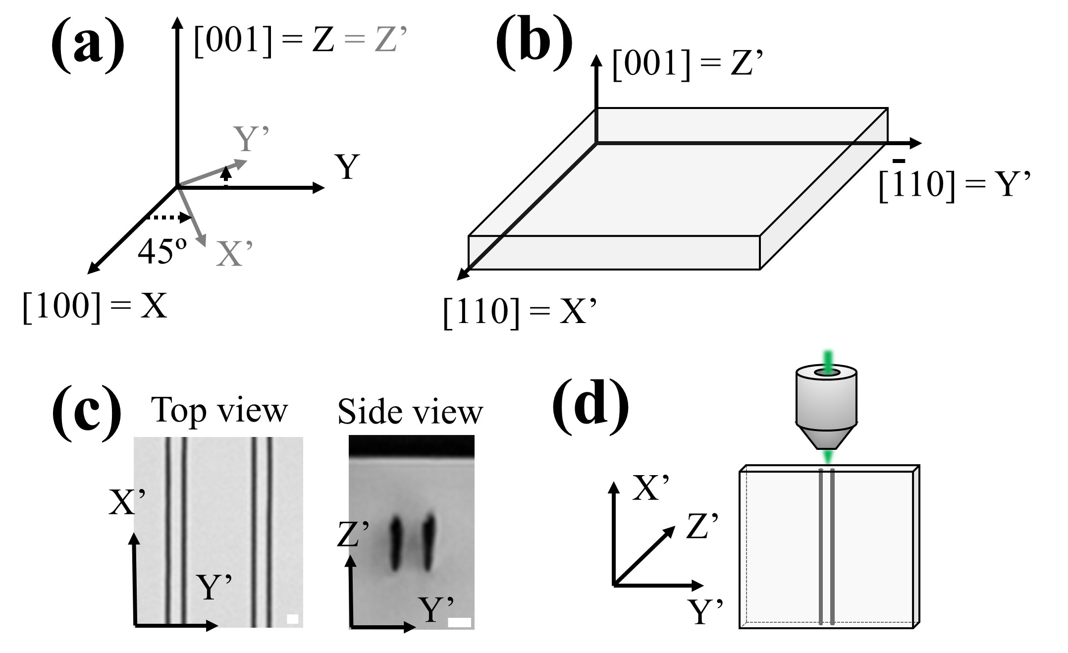
Finally, Raman spectra were recorded using a Labram Aramis Jobin Yvon Horiba microRaman system with a DPSS laser source of 532 nm and equipped with a confocal microscope and an air-cooled CCD. The pinhole was 300 m. A 100 objective (0.8 NA) was used to focus the laser on the (110) plane of the sample as well as to collect the Raman signal (backscattering configuration), as shown in Fig. 1(d). This experimental configuration allows to detect the Raman modes needed to perform this study. The spatial resolution is below 1 m.
Cubic diamond lattice (space group ) has three optical phonons with symmetry at the center of the Brillouin zone. These phonons, in absence of strain in the lattice, have the same frequency ( = 1333 cm-1). The Raman intensity collected is given by the following expression, that depends on the Raman tensors () and the polarization vectors of the incident () and scattered () light:
| (1) |
The Raman tensors at the center of the Brillouin zone in the XYZ crystal system are:
Where accounts for the variation of the polarizability with the displacement of the atoms in the lattice Mildren and Rabeau (2013). For the coordinate system of our diamond sample X’Y’Z’ these tensors will be transformed as (rotation of 45 around the Z axis):
It is well known that when stress is applied to the diamond crystal, the cubic symmetry is removed and the degeneracy of the three optical phonons is lifted Ganesan, Maradudin, and Oitmaa (1970); Grimsditch, Anastassakis, and Cardona (1978); Ager III and Drory (1993); Von Kaenel et al. (1997); Anastassakis (1999); Gries et al. (2007). In order to obtain the new frequencies of the phonons at the zone-center related to the applied stress, the following secular equation, that derives from lattice dynamical equations Ganesan, Maradudin, and Oitmaa (1970) has to be solved:
| (2) |
Where , and are the deformation potential constants for diamond Grimsditch, Anastassakis, and Cardona (1978); Gries et al. (2007) (), and the eigenvalues are related to the former () and new frequencies of the three modes () Von Kaenel et al. (1997): . represents the components of the strain matrix, that are related to the stress by Hooke’s law: (i,j = 1,…, 6, being the compliance constants, following the matrix notation Nye (1985)).
For a cubic crystal, due to symmetry considerations, only three components are non-zero, having the following values for diamond Gries et al. (2007): GPa; GPa; GPa. As noted above, in the selected scenario of our waveguide, we are going to study the Raman signal in backscattering configuration from the (110) surface, considering that the stress produced by the two laser-written tracks has biaxial character in the (110) plane. The stress matrix referred to the X’Y’Z’ system is defined then as:
| (3) |
Where is the stress parallel to the [10] direction and is the stress parallel to the [001] direction. This matrix can be rotated into the XYZ crystal coordinates by applying a rotation of -45 around Z’ = Z axis:
| (4) |
Using this matrix, the strain components are calculated using Hooke’s law: By substituting in the secular equation (2), the eigenvalues are obtained:
| (5) |
| (6) |
| (7) |
In the case of the values reported by Von Kaenel et al. Von Kaenel et al. (1997) are reproduced. These results indicate that the applied stress lifted completely the triple degeneracy. Note that the sign convention for stress is that tensile stresses are positive while compressive are negative. From equation (1) and considering the conservation of the wavevector, we can derive the components that will be visible for backscattering from a (110) surface, which are shown in table I, in agreement with other studies Anastassakis et al. (1970); Von Kaenel et al. (1997) (note that Porto’s notation is used Arguello, Rousseau, and Porto (1969)).
| Geometry | Component //[001] | Component //[10] |
|---|---|---|
| ’(Y’Y’)X’ | ✓ | - |
| ’(Y’Z’)X’ | - | ✓ |
| ’(Z’Y’)X’ | - | ✓ |
| ’(Z’Z’)X’ | - | - |
From previous studies Ager III and Drory (1993), the out-of-plane component will show the most different value of shift. So the values obtained in equation (5) will be related to this component, whereas equation (6) and (7) are the components that will be measured in our experiments (//[001] and //[10] components).
In Fig. 2 the maps for the intensity and the shift of the diamond peak (from the fitting to Lorenztian curves) are shown. The Raman peak shows an intensity decrease in the laser-written tracks associated with disorder and change to the sp2-like phase induced by the laser Sotillo et al. (2016). The results obtained within the modified laser regions are not physically meaningful in this study as the fit of the diamond peak is more complex due to the presence of disorder and non-diamond carbon phases, so the lines position is marked in black in the maps of Fig. 2(b,c) by overlapping the region where the peak intensity is below 20%. In the region between the two lines, a small homogeneous broadening of the Raman peak from a width of 2.1 cm-1 to a width of 2.4 cm-1 is detected, related to the presence of stress Bergman and Nemanich (1995); Erasmus et al. (2011). The linewidth is similar along the guiding region, which is an indication of fairly uniform stress distribution.
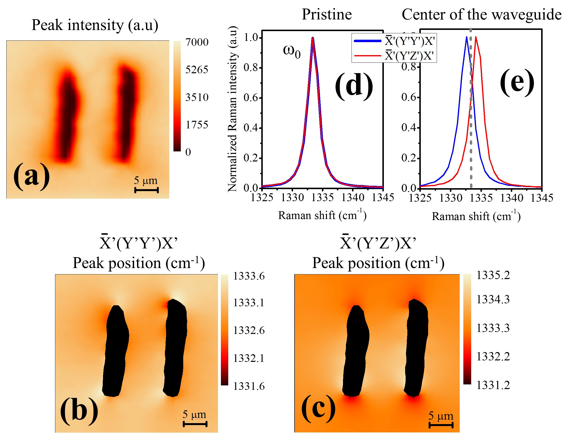
Following the selection rules of table I, if the configuration ’(Y’Y’)X’ is selected, the component parallel to [001] can be obtained, and is the one presented in Fig. 2(b). On the other hand, ’(Y’Z’)X’ configuration is shown in Fig. 2(c), which is associated with the component parallel to [10]. The shift of these two components (Fig. 2(d,e)) is a first indication that we can have stress with different character (tensile or compressive) in the [001] and [10] directions. In order to calculate the stress responsible for these shifts, equations (6) and (7) can be applied. A equation system must be solved in order to extract the values of and from the measured shifts:
| (8) |
At this point we have to consider the effect that the two laser lines can have on the surrounding material. The laser causes the amorphization of the crystal lattice and the transformation of sp3-diamond bonding into sp2 bondings Sotillo et al. (2016). This transformation generates a material with lower density inside the lines, producing a local volume expansion. Furthermore, the stress produced in the [10] direction () will be compressive, whereas in the perpendicular direction there will be a shear tensile stress (). Taking this into account, we associate the correct component and to the measured Raman components, and the calculated stress for each point in the map is shown in Fig. 3(a,b). In these maps it can be observed that has a compressive character between the two lines, whereas is mainly tensile. The sign of both stresses is inverted at the top and bottom tips of the lines (in a similar way to the theoretical study covering lithium niobate Burghoff, Nolte, and Tünnermann (2007)). From the vertical line profile of both stresses and measured at the center of the waveguide (Fig. 3(c)), it can be observed that the maximum value for both is located near the center of the waveguide.
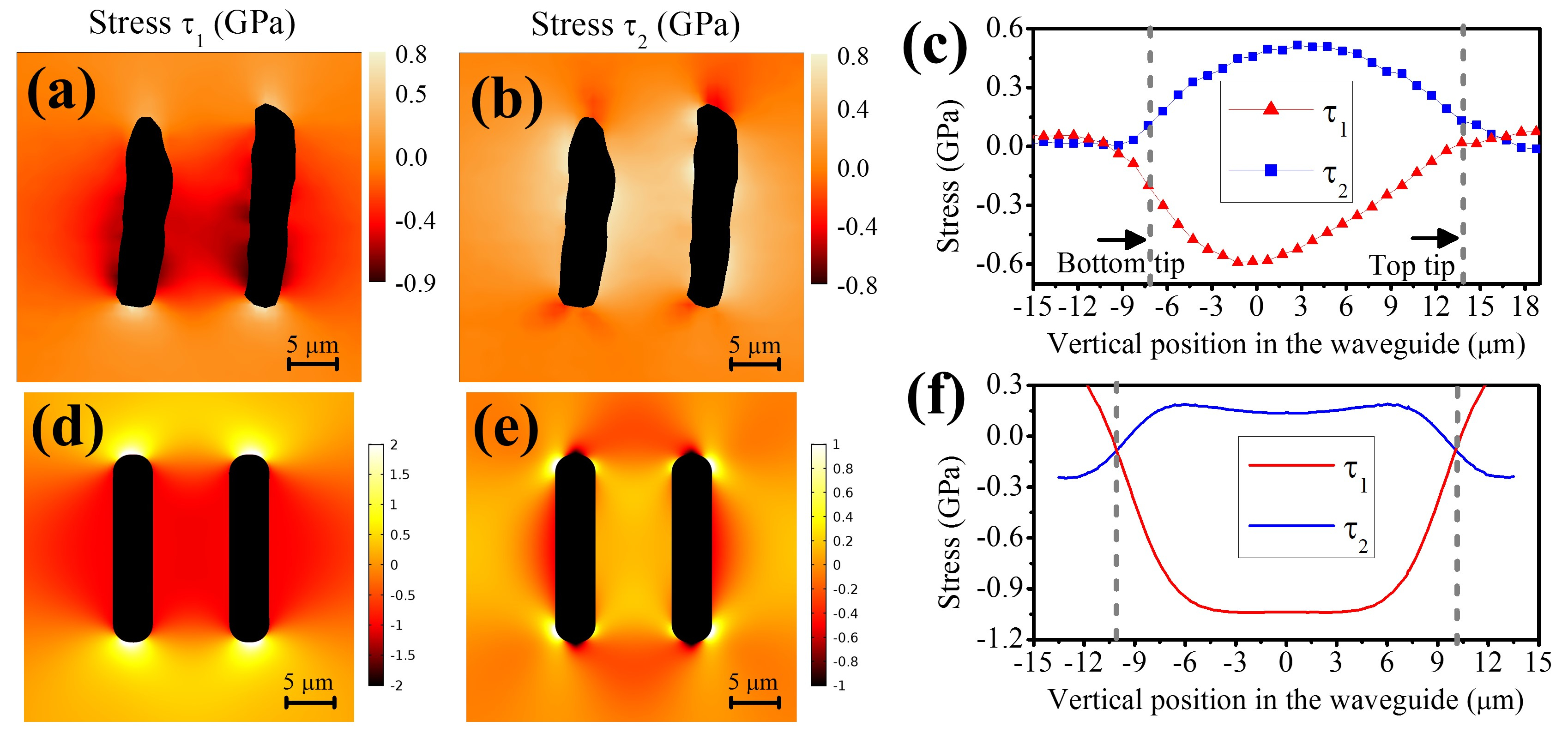
The calculated stresses are compared to those obtained from 2D Finite Element simulations of the constrained expansion of two amorphous carbon inclusions in a diamond matrix. The adopted procedure is described in Bosia et al.Bosia et al. (2013) and in Battiato et al. Battiato et al. (2016). To approximate the real geometry, two parallel rectangles with filleted corners are considered. The simulated and stress distributions, shown in Fig. 3 (d-f), correctly reproduce those observed experimentally. The small discrepancies and the asymmetry between the curves of and in Fig. 3(c) can be attributed to the simplified geometry in the simulations and possible inhomogeneities in material properties in the amorphized regions.
Once the stresses have been calculated from the measured shift of the Raman peak, the change in the refractive index can be obtained following the same strategy as Burghoff et al. Burghoff, Nolte, and Tünnermann (2007). Stress values are related to the refractive index through the piezooptic tensor :
| (9) |
As for the compliance tensor, due to the symmetry of the diamond crystal structure, only three components of the piezooptic tensor are non-zero: Pa; Pa; Pa Nye (1985). Previous experimental studies have shown that tensile hydrostatic pressure produces an increase in the refractive index of diamond Waxler and Weir (1965); Fontanella et al. (1977); Balzaretti and Da Jornada (1996). This effect is related to an increment of the electronic polarizability overbalancing the reduction of the density Waxler and Weir (1965), and has been observed in other materials, such as MgO, SiC or sapphire Waxler and Weir (1965); Balzaretti and Da Jornada (1996); Jones, Vaughan, and Gupta (2001). Here we have a biaxial stress, so the different components of the tensor must be calculated to assess the character of the refractive index change. Using equation (9) and the values of stress and , we can obtain the refractive index profile across the waveguide for the polarization parallel to [001] (Fig. 4(a)). A well localized region of increased refractive index is visible. Comparing the map of the refractive index change with the image of an optical mode (Fig. 4(c)), we can see that the mode is located at the same position as the increased refractive index region. For the polarization parallel to [10] the refractive index decreases in the guiding region.
From the map in Fig. 4(a), we can see that the optical mode is confined in the horizontal direction by the presence of the two laser-written lines which act as barriers due the decrease expected in these regions. In vertical direction, light is confined due to the stress-induced change in the refractive index. At the center of the waveguide, the calculated is .
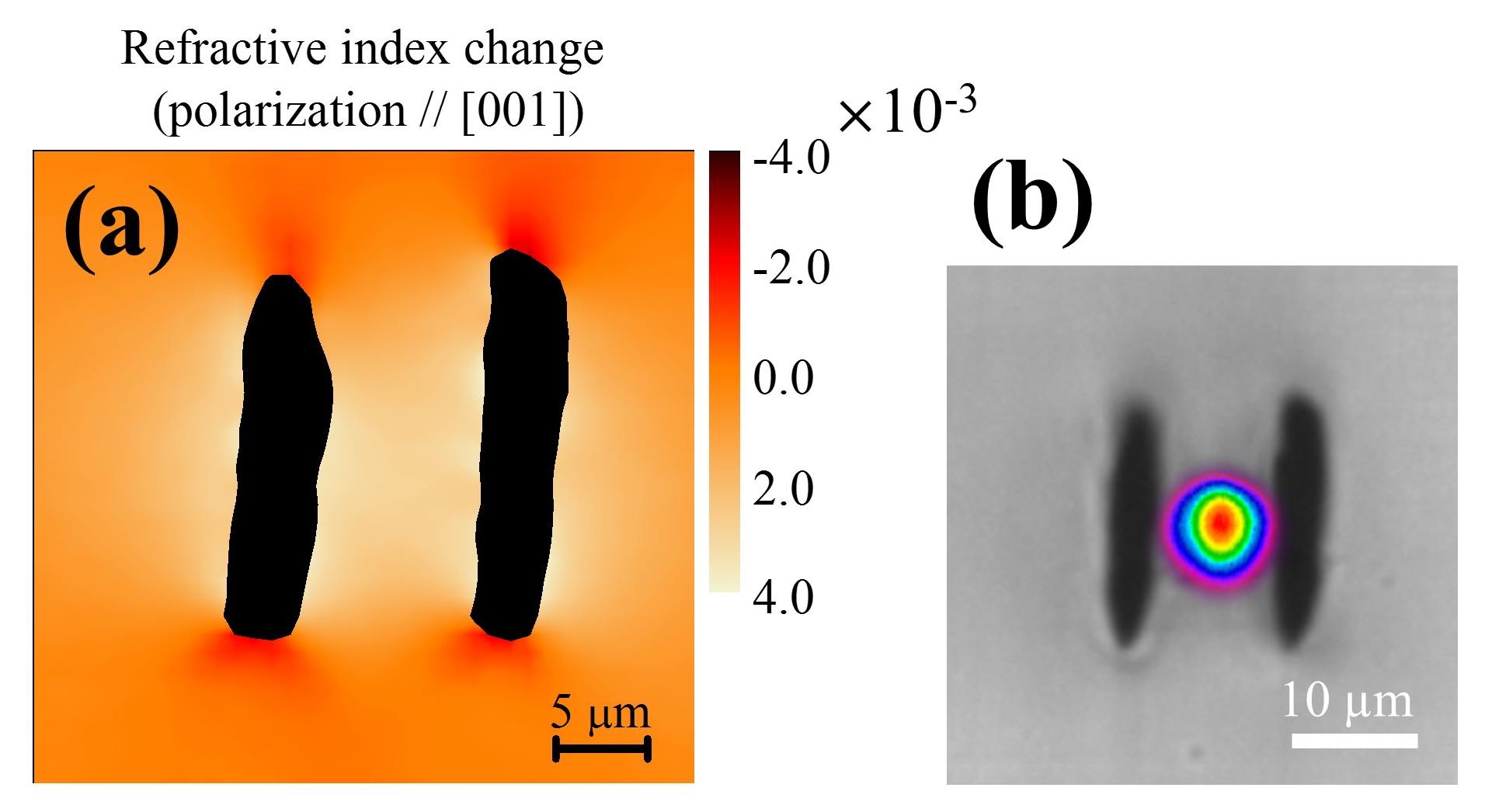
Finally, from the results we have obtained, we can gain a deeper understanding of the polarization behavior of the waveguides. We have reported before that the TM mode is guided, whereas the TE is not Sotillo et al. (2016). The TM mode will have the polarization parallel to the [001] crystallographic direction in the waveguides. So this polarization experiences an increase in the refractive index within the central region between the two barriers (Fig. 4(a)), and the mode is confined. On the other hand, the polarization parallel to [10] sees a decrease in the refractive index and thus the TE mode does not meet the conditions to be guided.
In conclusion, we have described the use of polarized Raman spectroscopy to obtain information about the stress distribution and refractive index change in diamond waveguides fabricated with femtosecond laser writing. We have shown that the optical mode is confined in the horizontal direction by the two laser-written lines, whereas in the vertical direction it is confined by the stress-induced refractive index change. The polarization behavior of the waveguides is explained from the stress created in the guiding region. This study provides a useful framework to design the properties of the diamond waveguides by changing the femtosecond laser writing parameters. The method can be extended to analyze stress-induced femtosecond laser written waveguides with different geometries in diamond as well as in other crystals.
The authors acknowledge support from FP7 DiamondFab CONCERT Japan project, DIAMANTE MIUR-SIR grant and FemtoDiamante Cariplo ERC reinforcement grant. We thank Prof. Guglielmo Lanzani and Dr. Luigino Criante for the use of the FemtoFab facility at CNST - IIT Milano for the laser fabrication experiments. We thank Prof. Roberto Osellame for access to waveguide characterization facilities. We thank Dr. Patrick Salter for helpful scientific discussions.
References
- Aharonovich et al. (2011) I. Aharonovich, S. Castelletto, D. A. Simpson, C. H. Su, A. D. Greentree, and S. Prawer, Reports on progress in Physics 74, 076501 (2011).
- Neumann et al. (2013) P. Neumann, I. Jakobi, F. Dolde, C. Burk, R. Reuter, G. Waldherr, J. Honert, T. Wolf, A. Brunner, J. H. Shim, et al., Nano letters 13, 2738–2742 (2013).
- Nguyen et al. (2017) C. T. Nguyen, R. E. Evans, A. Sipahigil, M. K. Bhaskar, D. D. Sukachev, V. N. Agafonov, V. A. Davydov, L. F. Kulikova, F. Jelezko, and M. D. Lukin, arXiv preprint arXiv:1708.05419 (2017).
- Schirhagl et al. (2014) R. Schirhagl, K. Chang, M. Loretz, and C. L. Degen, Annual review of physical chemistry 65, 83–105 (2014).
- Aharonovich, Greentree, and Prawer (2011) I. Aharonovich, A. D. Greentree, and S. Prawer, Nature Photonics 5, 397–405 (2011).
- Olivero et al. (2005) P. Olivero, S. Rubanov, P. Reichart, B. C. Gibson, S. T. Huntington, J. Rabeau, A. D. Greentree, J. Salzman, D. Moore, D. N. Jamieson, et al., Advanced Materials 17, 2427–2430 (2005).
- Khanaliloo et al. (2015) B. Khanaliloo, H. Jayakumar, A. C. Hryciw, D. P. Lake, H. Kaviani, and P. E. Barclay, Physical Review X 5, 041051 (2015).
- Burek et al. (2012) M. J. Burek, N. P. de Leon, B. J. Shields, B. J. Hausmann, Y. Chu, Q. Quan, A. S. Zibrov, H. Park, M. D. Lukin, and M. Lončar, Nano letters 12, 6084–6089 (2012).
- Lagomarsino et al. (2010) S. Lagomarsino, P. Olivero, F. Bosia, M. Vannoni, S. Calusi, L. Giuntini, and M. Massi, Physical review letters 105, 233903 (2010).
- Sotillo et al. (2016) B. Sotillo, V. Bharadwaj, J. P. Hadden, M. Sakakura, A. Chiappini, T. T. Fernandez, S. Longhi, O. Jedrkiewicz, Y. Shimotsuma, L. Criante, R. Osellame, G. Galzerano, M. Ferrari, K. Miura, R. Ramponi, P. E. Barclay, and S. M. Eaton, Scientific reports 6, 35566 (2016).
- Courvoisier, Booth, and Salter (2016) A. Courvoisier, M. J. Booth, and P. S. Salter, Applied Physics Letters 109, 031109 (2016).
- Bharadwaj et al. (2017) V. Bharadwaj, A. Courvoisier, T. T. Fernandez, R. Ramponi, G. Galzerano, J. Nunn, M. J. Booth, R. Osellame, S. M. Eaton, and P. S. Salter, Opt. Lett. 42, 3451–3453 (2017).
- Hadden et al. (2017) J. P. Hadden, V. Bharadwaj, B. Sotillo, S. Rampini, R. Osellame, R. J. Witmer, H. Jayakumar, T. T. Fernandez, A. Chiappini, C. Armellini, M. Ferrari, R. Ramponi, P. E. Barclay, and S. M. Eaton, arXiv preprint arXiv:1701.05885 (2017).
- Davis et al. (1996) K. M. Davis, K. Miura, N. Sugimoto, and K. Hirao, Optics letters 21, 1729–1731 (1996).
- Eaton et al. (2005) S. M. Eaton, H. Zhang, P. R. Herman, F. Yoshino, L. Shah, J. Bovatsek, and A. Y. Arai, Optics Express 13, 4708–4716 (2005).
- Gattass and Mazur (2008) R. R. Gattass and E. Mazur, Nature photonics 2, 219–225 (2008).
- Chen and Aldana (2014) F. Chen and J. R. Aldana, Laser & Photonics Reviews 8, 251–275 (2014).
- Burghoff, Nolte, and Tünnermann (2007) J. Burghoff, S. Nolte, and A. Tünnermann, Applied Physics A 89, 127–132 (2007).
- Eaton et al. (2008) S. M. Eaton, C. A. Merchant, R. Iyer, A. Zilkie, A. S. Helmy, J. S. Aitchison, P. R. Herman, D. Kraemer, R. J. D. Miller, C. Hnatovsky, et al., Applied Physics Letters 92, 081105 (2008).
- Ródenas et al. (2009) A. Ródenas, L. M. Maestro, M. O. Ramírez, G. A. Torchia, L. Roso, F. Chen, and D. Jaque, Journal of Applied Physics 106, 013110 (2009).
- Benayas et al. (2011) A. Benayas, W. F. Silva, A. Ródenas, C. Jacinto, J. V. de Aldana, F. Chen, Y. Tan, R. R. Thomsom, N. D. Psaila, D. T. Reid, G. A. Torchia, A. K. Kar, and J. D., Applied Physics A 104, 301–309 (2011).
- Oberson et al. (1998) P. Oberson, B. Gisin, B. Huttner, and N. Gisin, Applied optics 37, 7268–7272 (1998).
- Eaton et al. (2011) S. M. Eaton, M. L. Ng, R. Osellame, and P. R. Herman, Journal of Non-Crystalline Solids 357, 2387–2391 (2011).
- Ferraro et al. (2007) P. Ferraro, L. Miccio, S. Grilli, M. Paturzo, S. De Nicola, A. Finizio, R. Osellame, and P. Laporta, Optics express 15, 14591–14600 (2007).
- Mildren and Rabeau (2013) R. Mildren and J. Rabeau, Optical engineering of diamond (John Wiley & Sons, 2013).
- Ganesan, Maradudin, and Oitmaa (1970) S. Ganesan, A. A. Maradudin, and J. Oitmaa, Annals of Physics 56, 556–594 (1970).
- Grimsditch, Anastassakis, and Cardona (1978) M. H. Grimsditch, E. Anastassakis, and M. Cardona, Physical Review B 18, 901 (1978).
- Ager III and Drory (1993) J. W. Ager III and M. D. Drory, Physical Review B 48, 2601 (1993).
- Von Kaenel et al. (1997) Y. Von Kaenel, J. Stiegler, J. Michler, and E. Blank, Journal of applied physics 81, 1726–1736 (1997).
- Anastassakis (1999) E. Anastassakis, Journal of applied physics 86, 249–258 (1999).
- Gries et al. (2007) T. Gries, L. Vandenbulcke, P. Simon, and A. Canizares, Journal of Applied Physics 102, 083519 (2007).
- Nye (1985) J. F. Nye, Physical properties of crystals: their representation by tensors and matrices (Oxford university press, 1985).
- Anastassakis et al. (1970) E. Anastassakis, A. Pinczuk, E. Burstein, F. H. Pollak, and M. Cardona, solid state Communications 8, 133–138 (1970).
- Arguello, Rousseau, and Porto (1969) C. A. Arguello, D. L. Rousseau, and S. P. S. Porto, Physical Review 181, 1351 (1969).
- Bergman and Nemanich (1995) L. Bergman and R. Nemanich, Journal of Applied physics 78, 6709–6719 (1995).
- Erasmus et al. (2011) R. Erasmus, J. Comins, V. Mofokeng, and Z. Martin, Diamond and Related Materials 20, 907–911 (2011).
- Bosia et al. (2013) F. Bosia, N. Argiolas, M. Bazzan, B. A. Fairchild, A. D. Greentree, D. W. Lau, P. Olivero, F. Picollo, S. Rubanov, and S. Prawer, Journal of Physics: Condensed Matter 25, 385403 (2013).
- Battiato et al. (2016) A. Battiato, M. Lorusso, E. Bernardi, F. Picollo, F. Bosia, D. Ugues, A. Zelferino, A. Damin, J. Baima, N. M. Pugno, et al., Acta Materialia 116, 95–103 (2016).
- Waxler and Weir (1965) R. M. Waxler and C. E. Weir, Journal of Research of the National Bureau of Standards. Section A. Physics and Chemistry 69A, 325 (1965).
- Fontanella et al. (1977) J. Fontanella, R. L. Johnston, J. H. Colwell, and C. Andeen, Applied optics 16, 2949–2951 (1977).
- Balzaretti and Da Jornada (1996) N. M. Balzaretti and J. A. H. Da Jornada, Solid State Communications 99, 943–948 (1996).
- Jones, Vaughan, and Gupta (2001) S. C. Jones, B. A. M. Vaughan, and Y. M. Gupta, Journal of applied physics 90, 4990–4996 (2001).