Spectroscopy of bulk and few-layer superconducting NbSe2 with van der Waals tunnel junctions
Tunnel junctions, a well established platform for high resolution spectroscopy of superconductors, require defect-free insulating barriers with clean engagement to metals on both sides. Extending the range of materials accessible to tunnel junction fabrication, beyond the limited selection which allows high quality oxide formation, requires the development of alternative fabrication techniques. Here we show that van-der-Waals (vdW) tunnel barriers, fabricated by stacking layered semiconductors on top of the transition metal dichalcogenide (TMD) superconductor NbSe2, sustain a stable, low noise tunneling current, and exhibit strong suppression of sub-gap tunneling. We utilize the technique to measure the spectra of bulk (20 nm) and ultrathin (3- and 4-layer) devices at 70 mK. The spectra exhibit two distinct energy gaps, the larger of which decreases monotonously with thickness and , in agreement with BCS theory. The spectra are analyzed using a two-band model modified to account for depairing. We show that in the bulk, the smaller gap exhibits strong depairing in an in-plane magnetic field, consistent with a high Fermi velocity. In the few-layer devices, depairing of the large gap is negligible, consistent with out-of-plane spin-locking due to Ising spin-orbit coupling. Our results demonstrate the utility of vdW tunnel junctions in mapping the intricate spectral evolution of TMD superconductors over a range of magnetic fields.
Superconductors of the transition metal dichalcogenide (TMD) family have seen a revival of interest subsequent to developments in device fabrication by mechanical exfoliation Xi_2016 ; Tsen2015a ; Ugeda2015a ; Staley2009a ; Lu_MoS2_2015 ; Saito_MoS2_2015 ; Lu_2017 . The isolation of ultrathin Tsen2015a ; Xi_2016 has yielded indications of a Berezinskii-Kosterlitz-Thouless transition, which occurs in 2D superconductors. Xi_2016 , gated Saito_MoS2_2015 ; Lu_MoS2_2015 and gated Lu_2017 devices also remain superconducting in in-plane magnetic fields well beyond the Pauli limit Clogston_1962 ; Chandrasekhar_1962 . (Here, is the superconducting energy gap, is the Landé g-factor and the Bohr magneton.) This is likely due to Ising spin-orbit coupling (ISOC): The broken inversion symmetry of the monolayer TMD in the plane is expected to lead to the formation of Cooper pairs whose constituent spins are locked in the out-of-plane direction, in a singlet configuration. Interestingly, zero-resistance states have been observed in parallel magnetic fields exceeding the Pauli limit even in few-layer devices, where inversion symmetry is recovered Xi_2016 . This suggests that the inter-layer coupling is not strong enough to overcome the out-of-plane spin-locking due to ISOC Xi_2016 , perhaps in part due to the presence of spin-layer locking Jones2014 .
These previous studies [1-7] used in-plane electronic transport at high magnetic field and temperatures close to to determine the upper critical field , which depends on the magnitude of the spin-orbit field . Tunneling spectroscopy can provide complementary information. For example, tunneling and other probes (see Ref. Noat2015 and references therein) suggest that (bulk) is a 2-band superconductor. The role of the 2nd band, and its response to magnetic field, can be addressed by tunnel spectroscopy but not transport measurements. Tunneling can also probe the effect of magnetic field at the full temperature range and in fields ranging from zero to .
To carry out tunneling measurements on devices of variable thickness, at variable magnetic field conditions, it is necessary to develop a device-based architecture suitable for integration with TMDs. Oxide-based tunnel barriers, such as those used since the days of Giaever Giaever1960a , have now reached technological maturity; however, there is a limited number of oxides which form high-quality insulating, non-magnetic barriers, and they do not grow well on all surfaces. It is therefore of interest to explore alternatives based on van der Waals (vdW) materials Geim2013 , ultrathin layers of which can be precisely positioned on many surfaces Dean2010 . Indeed, such barriers have proven effective when integrated with graphene Amet2012 ; Britnell2012 ; Chandni2016 and appear to be promising candidates for integration with TMD superconductors island2016thickness .
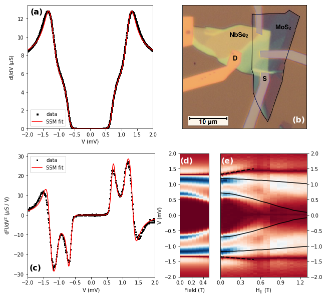
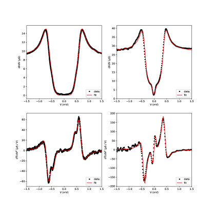
In this work, we fabricate Normal-Insulator-Superconductor (NIS) tunnel junctions with either or — both vdW materials — as the insulating barrier. The barrier material is placed on top of (hereafter ), a vdW superconductor with K, using the “dry transfer” fabrication technique Geim2013 ; Dean2010 . Crucially, such heterostructures can comprise flakes of varying thicknesses, from ‘bulk’ ( 6 layers) to few-layer, often within a single device. Fig. 1b shows a typical junction consisting of a 20nm-thick flake partially covered by a 4-5 layer thick barrier (cf. Supplementary Section 2). The junction has an area 1.6 , and we evaluate its transparency to be (Supplementary Section 5). Panel (a) shows the differential conductance as a function of obtained with the device, at . This spectrum has two striking features: first, the very low sub-gap conductance (), which indicates all bands crossing the Fermi energy are fully gapped. Second, the intricate structure of the quasiparticle peak differs from a standard BCS density-of-states (DOS) by having a relatively low peak and a shoulder at lower energies. The latter feature can be clearly seen in the second derivative (panel c) where the slope separates into a double peak feature, similar to STS scans of bulk Guillamon2008 ; Noat2015 . Based on this similarity, this flake can be considered bulk in terms of the zero field superconducting properties, and is hence referred to as the ‘bulk’ sample.
Density functional theory calculations Johannes2006 , and ARPES data Yokoya2001a show that the dispersion of consists of 5 independent bands which cross the Fermi energy. Of these, four are Nb-derived bands with roughly cylindrical Fermi surfaces, centered at the and points. The fifth is derived from the Se orbitals, which give rise to a small ellipsoid pocket around the point. Ref Noat2015 uses a two-band model to fit tunneling data, which can be justified noting that the Se and Nb-derived bands differ in the density of states and value of the electron-phonon coupling parameter Kiss2007 . We follow Ref Noat2015 in fitting our data using the same two-band model, which was developed in various forms by Suhl Suhl1959 , Schopohi Schopohi1977a and McMillan McMillan1968 (below ‘SSM’).
The model entails a self-consistent solution to the coupled equations for the energy dependent order parameters in the two bands :
| (1) |
describes the intrinsic gap within each band , that is generated by the electron-phonon coupling and by the scattering rates of quasiparticles between the bands . The extension of the two-band model to include Abrikosov-Gor’kov depairing AbrikosovA.A.1961ContributionImpurities ; Maki1964TheCurrents ; Levine1967DensityTunneling ; Millstein1967TunnelingField — via the terms with — was done by Kaiser and Zuckermann Keiser1970 . Here, depairing is due to magnetic field; thus, are set to 0 when no magnetic field is applied. The DOS of each band is then given by
| (2) |
where is the DOS at the Fermi energy in the normal state in band . The parameter , incorporates band-anisotropy. This anisotropy also affects the effective fit temperature (), which is higher than the sample temperature. Our fit indicates the presence of two independent order parameters. The larger, can be determined with high fidelity. The smaller order parameter , can not be determined unambiguously, and could have any value between 0 and 0.3 meV. The suppressed intrinsic superconductivity in the second band is consistent with a band with small density of states and weak electron-phonon coupling. The Se-band, having these properties Kiss2007 , is thus a candidate for the 2nd band.
We next investigate the evolution of the tunneling spectra vs. in-plane magnetic field (Figure 1e). The bulk sample appearing in Figure 1 is thick enough to accommodate Meissner currents leading to orbital depairing. We track the peaks in , which are associated with the two gaps. The high energy peak in depends weakly on the field, whereas the low energy peak evolves nonlinearly towards lower energies. This trend persists up to which we interpret as . Although is a clean-limit superconductor (coherence length mean free path), the evolution of the low energy gap in does not agree with the relevant, Doppler shift model Fulde1969book . Instead, the magnetic field evolution of its features towards lower energies is well-reproduced by the diffusive Kaiser-Zuckermann (KZ) model (Figure 1d), assuming a depairing parameter quadratic in . For a thin sample of thickness , tinkham1996introduction , with the diffusion coefficient, nm and the penetration length 230 nm Garoche1976a . We find 640 eV at 1 T, corresponding to 40 cm2/s. The model therefore yields a very large value for the diffusion coefficient , indicating a large Fermi velocity. This lends further support to the identification of this feature with the Se-derived band, where is 4-5 times larger than in the Nb-derived bands Kiss2007 . In contrast, the high energy quasiparticle peak moves only slightly and linearly to higher energies at low (dashed line in Figure 1e). From this, we estimate m/s. This indicates that a comprehensive description of the field evolution of the full spectrum would require a model with arbitrary disorder bridging clean and diffusive limits.
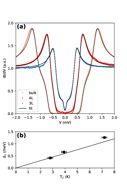
Our methods allow us to carry out a straightforward comparison of the tunneling spectra from devices with different thicknesses. Figure 2a shows differential conductance curves taken by tunneling into ultra-thin flakes (3 layers, 4 layers), in comparison to the of the bulk flake discussed above 111The 4-layer junction includes a small trilayer, but this has no apparent effect on the tunneling spectrum.. The spectra of the thin devices are in good agreement with the SSM model. We extract the values of from these fits, and separately evaluate using the temperature dependence of the tunneling conductance (details in Supplementary Section 5). We find that increases with (Figure 2b), however, deviating slightly from the BCS result . This deviation is plausible due to the multi-band nature of superconductivity in . The values measured here are lower than those reported elsewhere Xi_2016 ; Frindt , likely due to higher disorder in our sample Finkelshtein1987 ; Finkelshtein1994 ; Goldman . Note that, based on Ref. Frindt , it would seem that the dependence on number of layers seen by all works to date is not due to strain or other substrate effects.
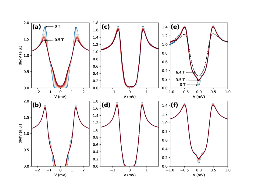
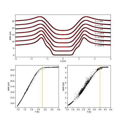
We now turn to the response of the ultrathin devices to in-plane magnetic fields. Figure 3 shows the tunneling spectra for the bulk device (panel a) and for the 4-layer and 3-layer devices (panels b and c, respectively). In the latter, unlike the bulk device, we find that the spectrum changes very little up to 3.5T (which is the maximal field where a compensation coil keeps a zero perpendicular field). In both 3 and 4 layer devices, there is a small reduction in the height of the quasiparticle peak; in the 3 layer device, the low energy spectrum exhibits a more intricate evolution (discussed below). Using the KZ model to quantify the reduction of the peak height, we find that the depairing term eV at 1T.
Since orbital depairing is quadratic in sample thickness, we expect it to be diminished in the 3 and 4 layer devices, allowing us to probe the spin-dependent interaction. The interaction of the spin with magnetic field should lead to Zeeman splitting of the spectrum, which we do not see. This could be due to two mechanisms. First, spin-orbit scattering can effectively randomize the spin, giving rise to a depairing parameter given by , where is the spin orbit scattering time tinkham1996introduction . Second, ISOC can align the spins in the out-of-plane direction with an effective field, , and the depairing term Lu_MoS2_2015 ; Xi_2016 . The first scenario can be ruled out, since it yields 50 fs, shorter than the scattering time Lu_MoS2_2015 . The ISOC case is more likely, and the depairing energy of at 1T (for the 3L device) yields T. Using (extracted by setting meV) we can estimate 30T, consistent with transport experiments Xi_2016 . We note that since the orbital term is not entirely suppressed, and we cannot estimate its contribution to the depairing, the estimate for is a lower bound. Further details concerning the possible interpretation of the depairing term are given in supplementary section 3.
The stability of the larger gap can even be demonstrated above the Pauli limit, for the 3 layer device. In Figure 3c we present the density of states of this sample above the Pauli limit by applying an in-plane field of 6.4T. At this field, our measurement system did not allow us to compensate for angle misalignment leading to small component of perpendicular field (0.2T) and possible vortex penetration. Nevertheless, the size of the gap remains unchanged. This lends further support to ISOC as the mechanism protecting superconductivity at high parallel fields.
The sub-gap spectrum of the 3-layer device appears to exhibit a secondary, well-formed small gap of , which is suppressed at . As we show in Figure 3(c,f), the KZ model reproduces this data remarkably well. Here, too, the depairing term is quadratic in , with 13 eV at 1 T. This value is to big to be interpreted in terms of orbital depairing. The observed depairing could alternatively be associated with spin-orbit-driven spin-flip scattering, with ps. This depairing shows that unlike the band with larger gap, this band is not protected by ISOC. This difference can be explained by associating the smaller order parameter with the Se-derived band. The outer gap, appearing immune to depairing, would then be associated with the Nb-derived -band. We note that this interpretation leaves open the question of the role of the Nb-derived -band. Addressing this question will require further spectral studies - in particular, of monolayer where the Se-derived band does not cross the Fermi energy.
Our results show that TMD semiconductors transferred on top of form stable tunnel barriers with a hard gap. We show that the SSM model, modified to include diffusive depairing, successfully reproduces the tunneling spectra in both the bulk and the ultrathin limits, at the presence of in-plane magnetic fields. This allows us to probe the effect of the spin and orbital degrees of freedom on the spectra, thereby differentiating between the responses of the different bands to the field. The large gaps, in the 3 and 4 layer devices, are remarkably stable to depairing by the in-plane field, exhibiting very small depairing energies (< 1 eV), which place a tight cap on the spin-depairing observed on this band, lending support to ISOC as the mechanism behind this stability. We suggest that our technique can be generalized to work with many other material systems, such as organic (super)conductors and other fragile systems which have hitherto not been investigated in tunneling spectroscopy.
Methods
The vdW tunnel junctions were fabricated using the dry transfer technique Castellanos-Gomez2014 , carried out in a glove-box (nitrogen atmosphere). flakes were cleaved using the scotch tape method, exfoliated on commercially available Gelfilm from Gelpack, and subsequently transferred to a substrate. and flakes were similarly exfoliated and thin flakes suitable for the formation of tunnel barriers were selected based on optical transparency. The barrier flake was then transferred and positioned on top of the flake at room temperature. Ti/Au contacts and tunnel electrodes were fabricated using standard e-beam techniques. Prior to the evaporation of the ohmic contacts the sample was ion milled for 15 seconds. No such treatment was done with the evaporation of the tunnel electrodes. All transport measurements were done in a 3He–4He dilution refrigerator with a base temperature of 70 mK. The AC excitation voltage was modulated at 17 Hz; its amplitude was 15V at all temperatures for the bulk device and 10V for the few-layer devices. Measurement circuit details are provided in Supplementary Section 1.
Acknowledgements
We thank P. Février and J. Gabelli for helpful discussions on tunnel barriers, and T. Cren for the same on . This work was funded by a Maimonïdes-Israel grant from the Israeli-French High Council for Scientific & Technological Research and by an ANR JCJC grant (SPINOES) from the French Agence Nationale de Recherche. H.S. acknowledges support by ERC-2014-STG Grant No. 637298 (TUNNEL) and Marie Curie CIG Grant No. PCIG12-GA-2012-333620. T.D. is grateful to the Azrieli Foundation for an Azrieli Fellowship. F.M. has received funding from the European Union’s Horizon 2020 research and innovation programme under the Marie Skłodowska-Curie Grant No. 659247. L.A. and M.K. are supported by the Israeli Science Foundation through Grant No. 1287/15.
Author contributions
T.D. fabricated the devices. C.Q.H.L., T.D. and M.A. performed the measurements. All the authors contributed to data analysis and the writing of the manuscript.
Competing financial interests
The authors declare no competing financial interests.
References
- (1) Xi, X. et al. Ising pairing in superconducting NbSe2 atomic layers. Nature Physics 12, 139–143 (2016).
- (2) Tsen, a. W. et al. Nature of the Quantum Metal in a Two-Dimensional Crystalline Superconductor. Nature Physics 1–8 (2015).
- (3) Ugeda, M. M. et al. Characterization of collective ground states in single-layer NbSe2. Nature Physics 12, 92–97 (2015).
- (4) Staley, N. E. et al. Electric field effect on superconductivity in atomically thin flakes of NbSe2. Physical Review B 80, 1–6 (2009).
- (5) Lu, J. M. et al. Evidence for two-dimensional Ising superconductivity in gated MoS2. Science 350, 1353–1357 (2015).
- (6) Saito, Y. et al. Superconductivity protected by spin–valley locking in ion-gated MoS2. Nature Physics 12, 144–149 (2015).
- (7) Lu, J. M. et al. A full superconducting dome of strong Ising protection in gated monolayer WS2. arXiv preprint arXiv:1703.06369 (2017).
- (8) Clogston, A. M. Upper Limit for the Critical Field in Hard Superconductors. Physical Review Letters 9, 266–267 (1962).
- (9) Chandrasekhar, B. S. A note on the maximum critical field of high-field superconductors. Applied Physics Letters 1, 7 (1962).
- (10) Jones, A. M. et al. Spin-layer locking effects in optical orientation of exciton spin in bilayer . Nature Physics 10, 130–134 (2014).
- (11) Noat, Y. et al. Quasiparticle spectra of 2H-NbSe2: Two-band superconductivity and the role of tunneling selectivity. Physical Review B 92, 1–18 (2015).
- (12) Giaever, I. Energy gap in superconductors measured by electron tunneling. Physical Review Letters 5, 147–148 (1960).
- (13) Geim, A. K. & Grigorieva, I. V. Van der Waals heterostructures. Nature 499, 419–425 (2013).
- (14) Dean, C. R. et al. Boron nitride substrates for high-quality graphene electronics. Nature Nanotechnology 5, 722–726 (2010).
- (15) Amet, F. et al. Tunneling spectroscopy of graphene-boron-nitride heterostructures. Physical Review B 85 (2012).
- (16) Britnell, L. et al. Electron tunneling through ultrathin boron nitride crystalline barriers. Nano Letters 12, 1707–1710 (2012).
- (17) Chandni, U., Watanabe, K., Taniguchi, T. & Eisenstein, J. P. Signatures of phonon and defect-assisted tunneling in planar metal-hexagonal boron nitride-graphene junctions. Nano Letters 16, 7982–7987 (2016).
- (18) Island, J. O., Steele, G. A., van der Zant, H. S. & Castellanos-Gomez, A. Thickness dependent interlayer transport in vertical mos2 josephson junctions. 2D Materials 3, 031002 (2016).
- (19) Guillamón, I., Suderow, H., Guinea, F. & Vieira, S. Intrinsic atomic-scale modulations of the superconducting gap of 2H-NbSe2. Physical Review B 77 (2008).
- (20) Johannes, M. D., Mazin, I. I. & Howells, C. A. Fermi-surface nesting and the origin of the charge-density wave in NbSe2. Physical Review B 73, 205102 (2006).
- (21) Yokoya, T. et al. Fermi surface sheet-dependent superconductivity in 2H-NbSe2. Science 294, 2518–20 (2001).
- (22) Kiss, T. et al. Charge-order-maximized momentum-dependent superconductivity. Nature Physics 3, 720–725 (2007).
- (23) Suhl, H., Matthias, B. T. & Walker, L. R. Bardeen-Cooper-Schrieffer Theory of superconductivity in the case of overlapping bands. Physical Review Letters 3, 552–554 (1959).
- (24) Schopohl, N. & Scharnberg, K. Tunneling Density of States for the Two-Band Model of Superconductivity. Solid State Communications 22, 37–1 (1977).
- (25) McMillan, W. L. Tunneling model of the superconducting proximity effect. Physical Review 175, 537–542 (1968).
- (26) Abrikosov A.A. & Gor’kov L.P. Contribution to the Theory of Superconducting Alloys with Paramagnetic Impurities. Soviet Physics JETP 12, 1243 (1961).
- (27) Maki, K. The Behavior of Superconducting Thin Films in the Presence of Magnetic Fields and Currents. Progress of Theoretical Physics 31, 731–741 (1964).
- (28) Levine, J. L. Density of States of a Short-Mean-Free-Path Superconductor in a Magnetic Field by Electron Tunneling. Physical Review 155, 373 (1967).
- (29) Millstein, J. & Tinkham, M. Tunneling into superconducting films in a magnetic field. Physical Review 158, 325–332 (1967).
- (30) Kaiser, A. B. & Zuckermann, M. J. McMillan Model of the Superconducting Proximity Effect for Dilute Magnetic Alloys. Physical Review B 1, 229–235 (1970).
- (31) Fulde, P. Tunneling phenomena in solids, chap. Gapless Superconducting Tunneling- Theory (Springer, 1969).
- (32) Tinkham, M. Introduction to superconductivity (Courier Corporation, 1996).
- (33) Garoche, P., Veyssié, J., P, M. & P, M. Experimental inverstigation of superconductivity in 2H-NbSe2 single crystal. Solid State Communications 19, 455–460 (1976).
- (34) The 4-layer junction includes a small trilayer, but this has no apparent effect on the tunneling spectrum.
- (35) Frindt, R. F. Superconductivity in Ultrathin NbSe2 Layers. Physical Review Letters 5, 299–301 (1972).
- (36) Finkel’shtein, A. M. Superconducting transition temperature in Amorphous Films. JETP 45, 37–40 (1987).
- (37) Finkel’shtein, A. M. Suppression of superconductivity in homogeneously disordered systems. Physica B 197, 636–648 (1994).
- (38) Goldman, A. M. & Marković, N. Superconductor-insulator transitions in the two-dimensional limit. Physics Today 51, 39–44 (1998).
- (39) Castellanos-Gomez, A. et al. Deterministic transfer of two-dimensional materials by all-dry viscoelastic stamping. 2D Materials 1, 011002 (2014).
- (40) Renner, C., Kent, A. D., Niedermann, P., Fischer & Lévy, F. Scanning tunneling spectroscopy of a vortex core from the clean to the dirty limit. Phys. Rev. Lett. 67, 1650–1652 (1991).
- (41) Sharvin, Y. V. A possible method for studying Fermi surfaces. JETP 48, 984–985 (1965).
- (42) Griffiths, D. J. Introduction to quantum mechanics (Pearson Education India, 2005).
- (43) Brinkman, W. F., Dynes, R. C. & Rowell, J. M. Tunneling Conductance of Asymmetrical Barriers. Journal of Applied Physics 41, 1915 (1970).
Supplemental Materials: Spectroscopy of bulk and few-layer superconducting NbSe2 with van der Waals tunnel junctions
S1 Details of the measurement setup and the fitting process
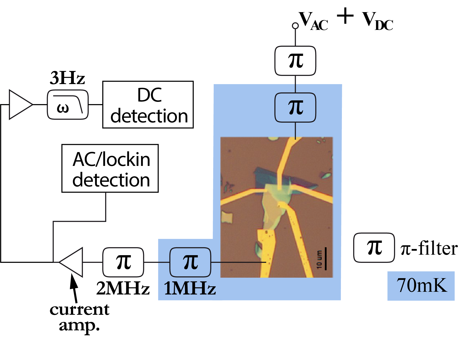
Figure S1 shows our measurement circuit in greater detail than was presented in the main text. All -filters at low temperature have cutoff frequencies of 1MHz while those at room temperature have cutoff frequencies of 2MHz. The amplitude of the AC excitation is 15V in all the figures of the main text. Measurements at lower showed that, between 2V and 15V, there was no discernible distortion of ; the higher excitation voltage was thus chosen in order to have a better signal-to-noise ratio.
To fit the resulting dI/dVs to the SSM model as discussed in the main text, the data was horizontally shifted, to account for zero bias drift, and divided by a dI/dV curve taken at T > TC. It was then symmetrized around zero bias, and fitted using least-squares method to the SSM model. The data shown in the figures, in the main text and in the supplementary, is either the original data as measured, or the data divided by a constant normalization factor, shifted horizontally by a constant bias.
S2 Thickness and structure of the tunnel barrier
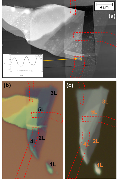
The high optical contrast between layers of different thickness of transition metal dichalcogenides (TMDs) allows easy identification of the thickness of the tunnel barrier. Figure S2 shows the optical image of the barrier on the PDMS immediately after it was exfoliated (panel c) and on top of the flake after the transfer procedure (panel b). Both show clearly that the source electrode was deposited above a region consisting of 4 and 5 layer thick . As a result of exponential dependence of the tunnel current on the barrier thickness, only the 4 layer part of the junction is significant to the measurement. Hence we expect the effective junction area to be 1.6 and the barrier thickness to be between 2.4 nm and 2.6 nm.
Contrary to the optical images, AFM does not provide a reliable measure of height between two different materials and cannot measure the thickness of the barrier. However AFM reveals some structures which are probably due to PDMS residue from the transfer process (panel a). A cross section of some of these features in the area of the junction shows height variation on the scale of 7 nm. The usual cleaning techniques of heat annealing cannot be used here due to the sensitivity of to heat. The effect of this structure is most likely to reduce the effective area of the junction to the non-contaminated region. As discussed below, the effective area of the junction is of the same order of magnitude as the observed area, showing the robustness of this method to imperfections.
S3 Fitting of the SSM model to the spectrum of ultra-thin NbSe2
The two band SSM can be used to fit spectrum obtained from 3- and 4- layers . The fits are shown in figure S3 and the fit parameters are given in table 1. It is clear that the value of decreases with a decreasing number of layers. In addition, the coupling constant , which is associated with the rate of scattering of electrons from the band with the larger coupling, also decreases with decreasing number of layers.
| Thickness | T | ||||||
|---|---|---|---|---|---|---|---|
| Bulk | 1.24 | 0.29 | 0.41 | 1.32 | 1 | 0.11 | 0.44 |
| 4 layers | 0.65 | 0.42 | 0.14 | 0.03 | 1 | 0.03 | 0.5 |
| 3 layers | 0.4 | 0 | 0.09 | 0.09 | 1 | 0.04 | 0.32 |
The KZ model extends the SSM model to describe the spectrum under the application of in-plane magnetic field. This requires the introduction of a depairing parameter for each band. We show the value of extracted from the model fit for each device in the table below. We stress that the observed change in the spectrum with magnetic field is very small in the case of the thin samples, and in the band with the larger gap of the bulk samples. Thus, the obtained values of should be treated as bounds, rather then accurate numbers. Further study, conducted at higher fields would allow for a more precise estimation.
The depairing represented by can originate from orbital depairing or from the interaction between the electrons’ spin the applied magnetic field. Interpreting the depairing in terms of diffusive orbital effect allows us to extract the diffusion constant, , as explained in the main text. Assuming a Fermi velocity m/sec, typical to bands, we can extract the elastic mean free path, and the time between scatterings, . The mean free path was previously found to be in the range 30-80 nm Renner1991a ; Haven1980. Table 2 show that this interpretation gives plausible values for all bands except the second band in the 3L device. The values for the second bands in the bulk and 4L device are slightly higher than expected. This can be resolved by assuming a higher Fermi velocity, consistent with their identification as originating from the Se derived band. In the 3L device, the depairing is too high to originate from orbital depairing, and has to be associated with spin-field interaction.
To interpret the depairing in terms of the interaction between the field and the spins, we note that away from the extreme paramagnetic limit, we should observe Zeeman splitting of the quasiparticle peaks. The effect can be suppressed by the spin-orbit interaction in one of the ways - spin flip during scattering process, that averages the projection of the spin on the magnetic field; and renormalization of the in-plane magentic field by the effective out-of-plane field generated by the Ising spin-orbit coupling. The former effect is quantified by a typical time for spin flip, , whereas the latter is quantified by a spin orbit energy. Both enter the KZ model through . Table 2 shows that for the bands 1,2 of the 4 layer device and band 1 of the 3 layer device, is shorter than the typical elastic scattering time, making this interpretation implausible.
| Thickness | [ev/T2] | [cm2/sec] | [nm] | [fsec] | [psec] | [meV] |
| Bulk, band 1 | 50 | 3 | 11 | 0.1 | - | - |
| Bulk, band 2 | 640 | 40 | 135 | 1.5 | - | - |
| 4 layers, band 1 | 0.8 | 6 | 18 | 0.2 | 0.08 | 8.2 |
| 4 layers, band 2 | 2 | 14 | 46 | 0.5 | 0.2 | 3.3 |
| 3 layers, band 1 | 0.5 | 6 | 20 | 0.2 | 0.05 | 13 |
| 3 layers, band 2 | 6 | 75 | 250 | 2.7 | 0.6 | 1.1 |
S4 Temperature dependent differential conductance
Figure S4a shows the differential conductance curves taken with the bulk sample at different temperatures. To fit the data, first the lowest temperature curve was fitted to the SSM model as discussed above. Then, the other curves were fitted to the model with the same parameters, where only the temperature and order parameters () were allowed to change. Best fit was obtained when the order parameters remained unchanged. Panels b and c show the zero bias conductance as a function of temperature for the three and four layer samples, respectively. This data was used to determine , as transport data was unavailable. The critical temperature was defined by 5% reduction in the conductance.
S5 Estimate of the barrier transparency
We can estimate the transparency of our tunnel barrier from the well-known expression from Sharvin Sharvin1965 :
| (S1) |
where is the junction conductance in the normal state, is the area of the junction, the Fermi momentum and the average transmission of each conductance channel. We measure 7S for 1.6 . in metals is usually and it is about half this value in . Taking the lower value, we get .
We can make an independent estimate of using the textbook WKB formula for a square barrier of thickness and height Griffiths2005 :
| (S2) |
where is the effective mass of the electron in the barrier, here .
The gap of few layer at the point in the Brilloiun zone is on the order of 2eV, whereas the effective mass is generally a fraction of 1. Taking 1eV, ( being the bare electron mass), and in the range 2.4–2.6nm we find –, consistent with the Sharvin estimate.
We can make a more rigorous estimate of (and thus ) by using Brinkman et al.’s result Brinkman1970TunnelingBarriers for the conductance across a trapezoidal barrier with diffuse boundaries, together with measurements of the high bias conductance of our junction:
| (S3) |
where is the voltage across the barrier, is the mean barrier height, the barrier height difference on the two sides of the trapezoid, the barrier width and . In these expressions, is in units of Å, while , and are in units of volts.
Far from the Fermi level, the conductance of our junction indeed rises (Figure S5). This rise is not perfectly parabolic and is likely due, in part, to factors other than barrier transparency and asymmetry. Therefore, fitting a parabola to the background, i.e. assuming that the rise is due almost entirely to the barrier, will give us a worst case scenario or minimum possible barrier height.
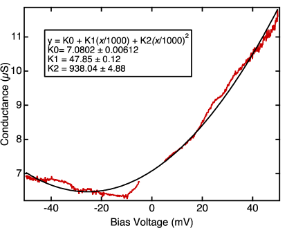
From the fit to our data to Equation S3 using = 20Å, we find 0.8V, not so different from what we assumed previously. If we use this, and 2.4–2.6nm as before, –.
Considering all of the above, is likely in the range or close to it.