Tunable Graphene Metasurface Reflectarray for Cloaking, Illusion and Focusing
Abstract
We present a graphene-based metasurface that can be actively tuned between different regimes of operation, such as anomalous beam steering and focusing, cloaking and illusion optics, by applying electrostatic gating without modifying the geometry of the metasurface. The metasurface is designed by placing graphene nano-ribbons (GNRs) on a dielectric cavity resonator, where interplay between geometric plasmon resonances in the ribbons and Fabry-Perot resonances in the cavity is used to achieve 2 phase shift. As a proof of the concept, we demonstrate that wavefront of the field reflected from a triangular bump covered by the metasurface can be tuned by applying electric bias so as to resemble that of bare plane and of a spherical object. Moreover, reflective focusing and change of the reflection direction for the above-mentioned cases are also shown.
I Introduction
Gradient metasurface is a planar arrangement of sub-wavelength scatterers of different shapes and sizes designed to structure wavefronts of reflected or transmitted optical beams by means of spatially varying optical responseHolloway et al. (2012); Yu and Capasso (2014); Jacob (2017); Kildishev et al. (2013); Meinzer et al. (2014). Light interaction with the metasurfaces defies conventional laws of geometrical optics, such as the Snell’s law or the law of reflection, and reveals a variety of non-trivial physical effects useful for practical applications. Particularly, efficient beam steering of the incident light in reflection and/or transmission modes was reported for metasurfaces operating both in narrow Yu et al. (2011a); Aieta et al. (2012a) and broad Ni et al. (2012); Sun et al. (2012); Li et al. (2015); Nemilentsau and Low (2017) frequency ranges. Moreover, pronounced polarization dependence of steering directions and/or amplitudes of beams deflected by metasurfaces was demonstrated Farmahini-Farahani and Mosallaei (2013); Pfeiffer and Grbic (2013); Pors et al. (2013a); Yin et al. (2013); Wu et al. (2014); Arbabi et al. (2015); Shaltout et al. (2015) thus paving the way for creating ultrathin optical polarizers, quarter and half wave platesYu et al. (2012); Zhao and Alù (2013); Ding et al. (2015). Great deal of attention has also been devoted to developing of viable alternatives to conventional focusing devices in transmission Memarzadeh and Mosallaei (2011); Aieta et al. (2012a); Chen et al. (2012); Monticone et al. (2013); Ni et al. (2013) (lenses) and reflection Li et al. (2012); Pors et al. (2013b); Veysi et al. (2015); Ma et al. (2016); Zhang et al. (2016); Fan et al. (2017) (parabolic reflectors) geometries. In fact, reflectarrays allow for the implementation of parabolic phase gradient along a planar surface thus avoiding technologically complicated process of creating parabolic surfaces for reflected light.
Recently it has been realized that metasurfaces can replace transformation opticsLi and Pendry (2008); Lai et al. (2009a); Fleury and Alu (2014) when it comes to implementing efficient cloaking devices. The essence of optical cloaking is to surround the object to be hidden by a material with carefully designed spatially varying dielectric permittivity (optical cloak) so that far-field radiation pattern of the object-cloak system is as close as possible to that of empty space. Efficient hiding of 2D and 3D bumps by metasurface carpet cloaks was reported Estakhri and Alù (2014); Estakhri et al. (2015); Orazbayev et al. (2015); Yang et al. (2016a); Tao et al. (2016); Cheng et al. (2016). The advantage of the metasurface based cloaking is that control of the polarization, phase and amplitude of the wave reflected by a cloaked object can be achieved Yang et al. (2016b) without modifying all the components of permittivity and permeability tensors which is required when using the transformation optics approach.
The operational characteristics (angle of beam steering, focal distance, angular efficiency, losses etc.) of optical devices based on metasurfaces designed using conventional dielectric or metal materials is typically predefined by the metasurface geometry and cannot be changed on-the-fly during the device operation. This might be a significant limitation when tuning of device characteristics is essential for the device operation, particularly, tunable steering angle for optical switches. Attempts to overcome this limitation using gate-tunable conducting oxides Huang et al. (2016), temperature-tunable nematic liquid crystals Sautter et al. (2015) or strain tunable elastic polymers Kamali et al. (2016) as metasurface building blocks were reported. Graphene plasmonic resonatorsLow and Avouris (2014); Grigorenko et al. (2012); Garcia de Abajo (2014); Bludov et al. (2013); Malard et al. (2009); Avouris et al. (2017); Christensen et al. (2011) provides viable alternativeFallahi and Perruisseau-Carrier (2012); Carrasco et al. (2013, 2015); Sherrott et al. (2017) to design of active metasurface that can be tuned by applying gate voltage. Dynamic tuning of Fermi energy in graphene plasmonic structures has been reported for optical switchingYu et al. (2015) and infrared beam steering via acoustic modulationChen et al. (2014). Active tuning of steering angle using graphene based metasurfaces operating in reflection regime was reportedYatooshi et al. (2015); Carrasco et al. (2015).
The gradient metasurfaces are typically designed in order to perform a particular specialized task, such as tuning, focusing or cloaking. In this paper, we demonstrate that it is possible to design a versatile active metasurface using gate-tunable graphene ribbonsYan et al. (2013); Ju et al. (2011) on an arbitrary substrate surface, which is capable of performing each of the above-mentioned specialized tasks depending on the electric bias profile across the surface of the metasurface, i.e. without changing the metasurface geometry. Particularly, we demonstrate that far-field distribution of the electric field of the wave reflected from a bump covered by such a metasurface can resemble either that of bare plane (cloaking case) or that of an object of a different shape (illusion), depending on the applied bias. In addition, we show that such wavefront engineering - as anomalous reflection and focusing - can also be achieved in conjunction with cloaking and illusion.
In what follows, we discuss general metasurface design strategy in Section II, followed by theoretical and simulation results for the above-mentioned functionalities in Section III-V. Lastly, we end with some general discussions on experimental realization and performance issues of the device in Section VI.
II Design of the Metasurface
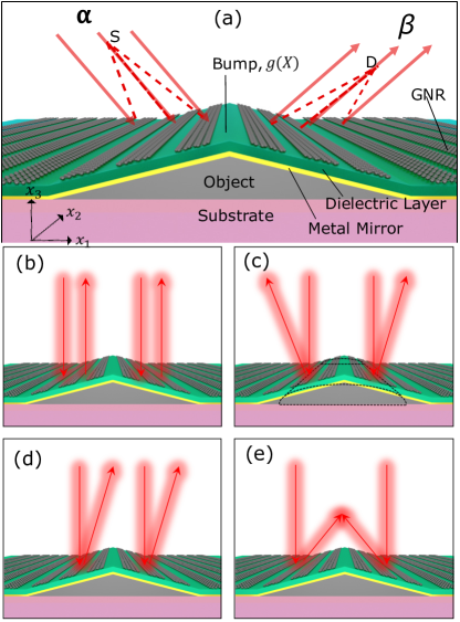
Fig. 1a shows a schematic of the graphene based metasurface device. In general, the metasurface can be implemented on a non-planarized surface. At the desired frequencies, mid-infrared light incident on the metasurface can be reflected in non-trivial fashion to achieve various functionalities. For example, the light can be reflected as if the surface is planar (see Fig. 1b) or disguised as a different surface morphology (see Fig. 1c). The former is often referred to as cloaking in the literature Ni et al. (2015); Chen and Alu (2011), while the latter as illusion opticsLai et al. (2009b). The light can also be anomalously reflected to far field as plane wave in predetermined direction (see Fig. 1d), or onto a focal point at the near field (see Fig. 1e), all achieved on a non-planar substrate.
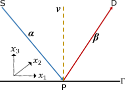
The general implementation of these various reflection modes can be achieved with the appropriate phase discontinuities, , at the graphene metasurface. The phase discontinuity for any arbitrary reflection beam wavefront can be derived from ray optics arguments. Let us consider a general surface in 3D space, with coordinates of a point on the surface defined as
| (1) |
where , , , (see Fig. 1a). The normal to the metasurface, , is
| (2) |
Suppose, and are unit direction vectors for incident and reflected waves. In absence of any phase discontinuity along the surface, we can write the vector form of conventional Snell’s law asLuneburg and Herzberger (1964)
| (3) |
which is equivalent to i.e is parallel to . Therefore, we can writeGutiérrez et al. (2017); Luneburg and Herzberger (1964)
where is a scalar factor, . When we have a phase discontinuity, given by a function , defined in the neighborhood of the surface, the generalized law of reflection in vector formGutiérrez et al. (2017) is given by (Appendix: A)
| (4) |
where is the free space wave number. Based on the desired operation, one would stipulate the required scattering beams and , and starting from Eq. (4) we can calculate the respective phase profiles . We defer these calculations to sections III-V.
In practice, design of a phase control metasurface involves two stepsScheuer (2017). First, a phase profile or phase mask for the desired wavefront modification is calculated and then individual pixels of the phase profile, which locally tailor the phase of the impinging wave, are designed. The scattering phase is achieved with graphene plasmonic nanoribbonsLow and Avouris (2014); Grigorenko et al. (2012); Garcia de Abajo (2014); Bludov et al. (2013); Avouris et al. (2017), whose plasmon resonance is tunable with doping or width. In this work, we fix the ribbon widths and vary the doping to achieve the desired phase .
Fig. 1a provides an illustration of the graphene nanoribbon based metasurface on a dielectric layer. There is a metal mirror below the dielectric layer separated at quarter wavelength distance from the graphene arrays. This maximizes the field at the graphene surface, hence enhancing light-matter interactionsCarrasco et al. (2015). To have total control over wavefront, the phase shift along the metasurface needs to encompass the full range. Graphene nanoribbon, with its Lorentzian-like response, provides a phase shift of only . The interference between the graphene resonator and the Fabry-Perot cavity provides the extra phase shift to make the total range of phase variation very close to Carrasco et al. (2015). From the phase profile function, , which we derive in Sections III-VI, we will be able to assign the required phase to each respective nanoribbon.
In this work, graphene conductivity is described with the finite temperature Drude formula which accounts for the intraband optical processes,
| (5) |
is the Fermi level of the nanoribbon, which is chosen according to the desired scattering phase, is the angular frequency taken to be equal to a free space wavelength of 22m, is the graphene relaxation time, is the electronic charge, K is the temperature. While choosing the value of relaxation time, the fact that plasmon damping increases due to interaction with optical phonons from graphene and substrate should be consideredYan et al. (2013). In this work, we assume a free space wavelength of 22m, which is significantly lower than the optical phonon energy (0.2eV) in graphene. Moreover, we assume a substrate that does not have surface optical phonons at the operating frequency, so the choice of relaxation time 0.1ps to ensure availability of 2 shift (see Appendix B) is justified. For example, CaF2 is transparent in mid-infrared. We use a value of = 0.6psYan et al. (2013). For the dielectric layer, we assume a lossless refractive index of =1.4 with thickness of 3.93m corresponding to the quarter wavelength condition.
Simulations are performed using Maxwell equation solver COMSOL MultiphysicsCOMSOL Multiphysics (2015) RF Module. We model each graphene ribbon in terms of its 2D current density. For this, we need to translate the spatial phase profile into corresponding conductivity profile. First, we define the position of each ribbon by the coordinates of their centers. Then using the phase profiles derived in Sections III-V, we get the discrete phase values for the ribbons. Using these phase values, we can determine the corresponding Fermi energy () for individual ribbons. Then, we get the required conductivity by putting the values in the Drude equation (Eq. (5)). Finally in COMSOL, we put this spatial conductivity profile defined for each nanoribbon as the conductivity of the surface current densities. A fixed ribbon width of 500nm and inter-ribbon distance of 750nm are used. is varied between 0.15-0.8eV. Perfectly Matched Layer (PML) conditions are used at the simulation domain boundaries and the metal reflector is modeled with a Perfect Electric Conductor (PEC).
III Cloaking: Specular and Anomalous Reflection
In this section we derive the phase function, , required for cloaking with specular or anomalous reflected beams. We assume that metasurface is parametrized by (1),(2). Following (4), we seek such that the metasurface reflects all incident rays with direction into rays with direction , where and are constant with respect to . Taking double cross product of Eq. (4) with yields
| (6) |
We seek such that is tangential to the surface, i.e. . Here, and in rest of the paper, the notation means derivative of with respect to . Therefore from (2),(III) we obtain
| (7) |
where
| (8) |
Eq. (7) is a system of three differential equations for unknown phase function, , written in vector form (see Appendix C for coordinate form), which can be reduced to two equations by taking into account that is in fact a function of two variables, , (see (1)). Using chain rule, we obtain
| (9) |
where , , and are defined by (7). Integrating, we obtain the phase:
| (10) |
with an arbitrary constant. For 2D geometry, i.e where the equations are independent of , the last equation can be written as
| (11) |
In terms of the incident angle and the reflection angle , we have , . So in terms of and , (11) becomes
| (12) |
This is the general phase equation for cloaking. When , this gives the phase for cloaking with specular reflection.
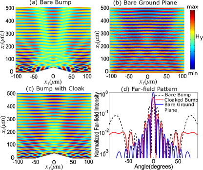
Fig. 2 shows simulation results for the specular cloaking case. We have a triangular shaped bump with base length 100m and height 40m as the object to be cloaked. Results are shown for normal incidence of light. Fig. 2a and 2b show scattered field (magnetic field ) plots for the bare bump and bare ground plane respectively. Next, the bump is cloaked by the metasurface designed with the above mentioned and the scattered field plot is shown in Fig. 2c. Accompanying angle resolved far-field intensity plots are shown in log-scale in Fig. 2d. As we can see, within the angular window of , the angular-resolved intensity spectrum for the cloaked bump and bare ground plane far-field match very well. The presence of side lobes in the far-field for the bare ground plane can be attributed to the finiteness of simulation domain. If we increase the size of the simulation domain, both the main lobes and side lobes become narrower and ideally, with infinitely large simulation domain, we can expect only one narrow main lobe.
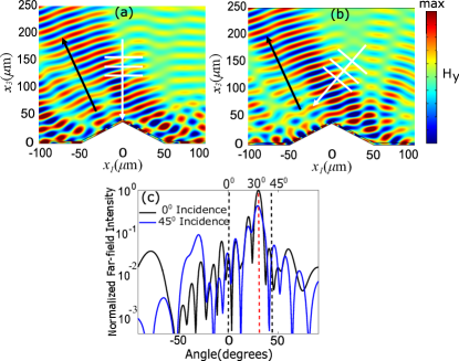
In similar fashion, we can also implement an extended version of the cloak, but with non-specular reflection angle. Fig. 3a demonstrates such implementation, designed with a angle of reflection off normal. In Fig. 3a and 3b, the scattered fields are shown for normal and angle of incidence, respectively. The white and black arrows show the incident and reflected wave directions. There are some distortions in the wavefronts predominantly due to specular reflections from the ground plane. In addition, we can also notice specular reflection on the right side of the bump. As we can see, the main beam is scattered at off normal per the design while power flow in specular directions ( and ) are more than an order of magnitude smaller.
IV Illusion Optics
Suppose that a surface in 3D space is parameterized by a function and no phase discontinuity is given on . The reflection of the rays by such a surface is governed by the standard Snell’s law of reflection,
| (13) |
where is a point on , , are the unit direction vectors for incident and reflected waves, and is the unit normal.
We consider another metasurface, , parameterized by (1), (2) and derive a phase discontinuity, , such that the metasurface does the same reflection job as the surface . That is, at each point the incident ray with unit direction is reflected into the ray with unit direction given in (13) . From (4) we then seek such that
| (14) |
As in Section III, making double cross product of this equation with and assuming that , yields
| (15) |
where we used (13) to obtain the second line. Equation (15) is a vector form of a system of three differential equations (see Appendix C for coordinate form), which once again can be simplified using the chain rule
| (16) |
where . Integrating system of two differential equations, (IV), we obtain (see Appendix D for details):
| (17) |
For the case where the configuration is independent of , formula (17) can be simplified to
| (18) |
Which gives the phase required to be applied along a surface to mimic the reflection pattern of another surface .
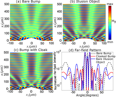
Fig. 4 shows the simulation results implementing the above mentioned for illusion optics. We have the same triangular bump as the object to be cloaked (i.e ) and a circular segment with chord length 100m and height 40m as the desired illusion object i.e . Fig. 4a and 4b show scattered field plots for the bare bump and illusion object respectively. When the triangular bump is cloaked by the designed metasurface, the scattering pattern becomes similar to that of the illusion object, which would make the triangular bump appear as a circular bump to an external observer. The field plot for the cloaked object is shown in Fig. 4c. Angle resolved far-field intensity plots are shown in Fig. 4d for comparison between these three cases. There is good agreement between the cloaked bump and illusion object in the far-field, especially within the angular window of .
V Reflective Focusing
In this section we consider focusing plane wave into a point using metasurface parametrized by (1),(2) (see Fig. 1e). Assuming that is the constant unit incident vector, we rewrite (4) as
where is the phase discontinuity along the metasurface, and is the unit reflected vector. Making the double cross product with yields
| (19) |
System of differential equations (19) (see Appendix C for coordinate form) can be simplified by calculating derivatives of phase function, , with respect to , , using the chain rule (see (9)),
with . Therefore, we obtain the phase
For 2D geometry independent of , and , the phase equation reduces to
| (20) |
In a similar way we can demonstrate (see Appendix E) that the phase discontinuity
| (21) |
should be imposed on the metasurface for focusing rays radiated by a point source located at .
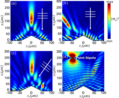
Simulation results for reflective focusing of incident parallel beams (plane wave) and point dipole source are shown in Fig. 5. In scattered field intensity plots of Fig. 5a, 5b and 5c, we have incident parallel beams focused to a point at a distance of 150m from the base of the triangular bump (i.e ground plane). First we consider normal incidence. Fig. 5a and Fig. 5b shows simulation results for normal incidence. Lastly, we consider oblique incidence with angle in Fig. 5c. Direction of incidence is shown by white arrows and position of the focusing point is indicated by ‘’. Flat gradient metasurfaces allow high numerical aperture (NA) diffraction limited focusing without spherical abberationAieta et al. (2012a); Yu and Capasso (2014). The size of the focal spot in Fig. 5a, b and c is comparable to the free space wavelength of 22m.
In Fig. 5d, an example of focusing of a point source is shown. The source is at (-50,250)m and focusing point is at (50,150)m. The point source is modeled by a electric point dipole in COMSOL with its dipole moment oriented along -direction. As there is no straight forward way to use a point source for scattered field calculation in COMSOL, we simulate for the total field instead with a point dipole acting as a point source. The plotted quantity in Fig. 5d, is the total field intensity i.e both incident and reflected fields are present. We can see higher intensity of field around the designed focus point indicating the focusing effect.
VI Discussion and Conclusion
Concluding, we demonstrated versatility of graphene-based metasurface that is capable of active switching between regimes of operation such as anomalous beam steering, focusing, cloaking and illusion optics simply by changing electric bias applied to graphene constituents of the metasurface without changing the metasurface geometry. These various functionalities are usually available in a disparate manner in the existing literature and we showed in this work that they can be described within a general framework for arbitrary surface morphology. The proposed approach, in particular to the context of graphene metasurface, makes perfect sense since graphene can be electrically tunable to achieve arbitrary phase function and conform to any surface morphology. As an example, we considered triangular bump covered by the graphene metasurface, made from graphene ribbons on the dielectric resonator, and demonstrated that, by applying an electric bias, the wavefront of the wave reflected by the bump can be tuned to match that of the bare plane (cloaking) or hemi-sphere (illusion optics). Moreover, the possibility of anomalous steering and focusing of the wave reflected by graphene metasurface covered bump was shown. The slight distortion of the metasurface far-field radiation pattern from that of the bare plane or hemi-sphere can be attributed to the specular reflection from the parts of metasurface not-covered by graphene ribbons, as well as to the fact that reflectivity of graphene ribbon depends on the applied electric bias. Finite size effects also show up in the field profile due to finiteness of simulation domain, discretization of metasurface and contribution from the apex of the triangleWei et al. (2017); Orazbayev et al. (2015). We expect that by optimizing the metasurface geometry these distortions can be reduced.
The device configuration considered here can be fabricated with conventional film deposition and nanopatterning technologies. The transfer of grapheneLee et al. (2010); Martins et al. (2013) onto bump structure and its patterning by electron beam lithography would be straightforward as demonstrated elsewhereWang et al. (2011); Hofmann et al. (2014). Nevertheless, there are a few issues that need to be addressed in terms of practical implementation. First of all, we should select a proper material for optical spacer, which is transparent over the concerned frequency range and compatible with conventional thin film deposition technologies. In addition, it is important to have small roughness on the film surface for the graphene transfer that follows. For mid-infrared applications, silicon oxide (SiO2)Rodrigo et al. (2015) and hexagonal boron nitride (hBN)Dai et al. (2015) have been popularly used as substrates for graphene, although plasmon losses due to strong plasmon-phonon coupling should be taken into consideration to determine the operation wavelength. Diamond-like carbonYan et al. (2013) and calcium fluoride (CaF2)Hu et al. (2016) can be good candidates as they do not have polar phonons in this frequency range. The issue of graphene and substrate losses are discussed in Appendix B. The insulating property and dielectric strength of the material used for the optical spacer becomes one of the important design parameters, from which the tunable range of graphene conductivity is largely determined. Another important aspect is addressing individual ribbons for separate doping. Since with other types of doping using chemical vapor and ion gel it is difficult to address individual ribbons, electrical doping by separate electrodes is necessary for the device. A recent workBarik et al. (2017) demonstrates that embedded local gating structures with graphene is experimentally feasible.
Acknowledgements.
This work is supported by a DARPA grant award FA8650-16-2-7640 and partially supported by NSF grant DMS-1600578.Appendix A Generalized Snell’s Law in Vector Form
Let rays of light be incident from point , at a point on a plane parallel to the plane, located at . Incident rays are then reflected to point . The normal to is . Therefore the incident unit vector from into a point on is and the reflected unit vector from into is . Since the ray is propagating in vacuum, from Fermat’s principle, the least optical paths for the incident and reflected rays are given by and and the corresponding accumulated phases are given by and respectively; where is the free space wave number and denotes the Euclidean distance. We introduce a phase discontinuity along . According to principle of stationary phase(Aieta et al., 2012b; Yu et al., 2011b), we then seek to minimize the total phase for in . Therefore at the extreme point on , by differentiating the total phase with respect to and , we must have
which from the definitions above of and can be rewritten as
for and . Since the normal , we therefore obtain the following expression of the generalized reflection law:
Notice that when there is no phase discontinuity, i.e. , we recover the standard reflection law in vector form. If is defined in a small neighborhood of the plane , i.e. is defined for all and for very small, then we can write the formula
| (22) |
where is a scalar.
Eq. (22) is the vector form of generalized Snell’s law for reflection.
Appendix B Effect of Loss on Phase
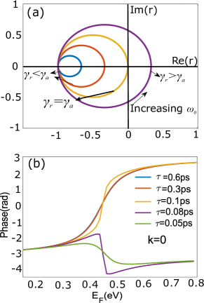
The attainable range of reflection phase is dependent on absorptive losses in the device. The reason for losing phase shift of with increased losses can be explained with arguments based on coupled mode theory (CMT). The device structure of graphene-substrate-metal creates an asymmetric Fabry-Perot resonator with a perfectly reflective mirror (metal) and a partially reflective mirror (graphene-dielectric layer interface). This can be effectively described as a one port single resonator, working at a resonant frequency of (Qu et al., 2015). According to CMT, when the resonator is excited by an external excitation of frequency , the reflection coefficient is given by(Haus, 1984)
Where is the rate of external or radiative losses and is the rate of internal of absorptive losses. Fig. 7a shows the plot of in complex plane for different with fixed . As can be seen on the plot, when absorptive losses are smaller than radiative losses (), covers all four quadrants in the complex plane and reflection phase covers the whole to range. This situation is called underdamped. But when absorptive loss surpasses radiative loss i.e , the phase of can no longer go from to and the system is called overdamped.
In our device, by changing , the plasmon resonance frequency is varied, as . The radiative losses () are constant as they are dependent on the dimensions of the device. The absorptive losses () are proportional to inverse of relaxation time, , and imaginary part of refractive index of the dielectric cavity, . Hence when is decreased or is increased, the system moves from underdamped to overdamped and the phase shift range is lost. In Fig. 7b, reflection phase is plotted as a function of for different relaxation times . The phase shift range becomes much smaller than when is decreased below ps. Similar behavior can be seen when is increased above . Both and are parameters related to total absorptive losses in the device. A similar phase behavior was observed in (Qu et al., 2015) for metal-insulator-metal (MIM) based metasurfaces.
Appendix C Coordinate representation of the vector equations for phase function
Coordinate form of the vector equation (8)
Coordinate form of the vector equation (15)
Coordinate form of the vector equation (19)
Appendix D Integrating of a system of differential equations (IV)
In this section we integrate a system of differential equations, (IV), obatined for the illusion optics case,
If and are , then the mixed partials and must be equal. Therefore to have a solution the following compatibility condition between , and must hold:
| (23) |
In fact, if (23) holds we will obtain the phase by integration as follows. To simplify the notation, set , so we need to solve the system
Integrating the first equation with respect to yields
Differentiating the last equation with respect to gives
So , and by integration . Therefore, we obtain
Appendix E Focusing from point source to point
Here we devise a metasurface for reflective focusing due to a point source. Let and be two points above the surface parameterized by (1), (2). We seek a phase discontinuity so that all rays incident from are reflected into . Then the incident unit direction equals and the reflected unit direction equals . From (4) we then seek so that
Following similar steps as discussed in Section V,
Writing in coordinates yields
Hence by the chain rule
with . Therefore we obtain the phase as
For 2D geometry independent of , and , the phase equation reduces to
| (24) |
References
- Holloway et al. (2012) C. L. Holloway, E. F. Kuester, J. A. Gordon, J. O’Hara, J. Booth, and D. R. Smith, IEEE Antennas and Propagation Magazine 54, 10 (2012).
- Yu and Capasso (2014) N. Yu and F. Capasso, Nature Materials 13, 139 (2014).
- Jacob (2017) S. Jacob, Nanophotonics 6, 137 (2017).
- Kildishev et al. (2013) A. V. Kildishev, A. Boltasseva, and V. M. Shalaev, Science 339, 1232009 (2013).
- Meinzer et al. (2014) N. Meinzer, W. L. Barnes, and I. R. Hooper, Nature Photonics 8, 889 (2014).
- Yu et al. (2011a) N. Yu, P. Genevet, M. A. Kats, F. Aieta, J.-P. Tetienne, F. Capasso, and Z. Gaburro, Science 334, 333 (2011a).
- Aieta et al. (2012a) F. Aieta, P. Genevet, M. A. Kats, N. Yu, R. Blanchard, Z. Gaburro, and F. Capasso, Nano Letters 12, 4932 (2012a).
- Ni et al. (2012) X. Ni, N. K. Emani, A. V. Kildishev, A. Boltasseva, and V. M. Shalaev, Science 335, 427 (2012).
- Sun et al. (2012) S. Sun, K.-Y. Yang, C.-M. Wang, T.-K. Juan, W. T. Chen, C. Y. Liao, Q. He, S. Xiao, W.-T. Kung, G.-Y. Guo, et al., Nano Letters 12, 6223 (2012).
- Li et al. (2015) Z. Li, E. Palacios, S. Butun, and K. Aydin, Nano Letters 15, 1615 (2015).
- Nemilentsau and Low (2017) A. Nemilentsau and T. Low, ACS Photonics 4, 1646 (2017).
- Farmahini-Farahani and Mosallaei (2013) M. Farmahini-Farahani and H. Mosallaei, Optics Letters 38, 462 (2013).
- Pfeiffer and Grbic (2013) C. Pfeiffer and A. Grbic, Applied Physics Letters 102, 231116 (2013).
- Pors et al. (2013a) A. Pors, O. Albrektsen, I. P. Radko, and S. I. Bozhevolnyi, Scientific Reports 3, 2155 (2013a).
- Yin et al. (2013) X. Yin, Z. Ye, J. Rho, Y. Wang, and X. Zhang, Science 339, 1405 (2013).
- Wu et al. (2014) C. Wu, N. Arju, G. Kelp, J. A. Fan, J. Dominguez, E. Gonzales, E. Tutuc, I. Brener, and G. Shvets, Nature Communications 5 (2014).
- Arbabi et al. (2015) A. Arbabi, Y. Horie, M. Bagheri, and A. Faraon, Nat Nano 10, 937 (2015).
- Shaltout et al. (2015) A. Shaltout, J. Liu, A. Kildishev, and V. Shalaev, Optica 2, 860 (2015).
- Yu et al. (2012) N. Yu, F. Aieta, P. Genevet, M. A. Kats, Z. Gaburro, and F. Capasso, Nano Letters 12, 6328 (2012).
- Zhao and Alù (2013) Y. Zhao and A. Alù, Nano Letters 13, 1086 (2013).
- Ding et al. (2015) F. Ding, Z. Wang, S. He, V. M. Shalaev, and A. V. Kildishev, Acs Nano 9, 4111 (2015).
- Memarzadeh and Mosallaei (2011) B. Memarzadeh and H. Mosallaei, Optics Letters 36, 2569 (2011).
- Chen et al. (2012) X. Chen, L. Huang, H. Mühlenbernd, G. Li, B. Bai, Q. Tan, G. Jin, C.-W. Qiu, S. Zhang, and T. Zentgraf, Nature Communications 3, 1198 (2012).
- Monticone et al. (2013) F. Monticone, N. M. Estakhri, and A. Alù, Physical Review Letters 110, 203903 (2013).
- Ni et al. (2013) X. Ni, S. Ishii, A. V. Kildishev, and V. M. Shalaev, Light: Science and Applications 2, e72 (2013).
- Li et al. (2012) X. Li, S. Xiao, B. Cai, Q. He, T. J. Cui, and L. Zhou, Optics Letters 37, 4940 (2012).
- Pors et al. (2013b) A. Pors, M. G. Nielsen, R. L. Eriksen, and S. I. Bozhevolnyi, Nano Letters 13, 829 (2013b).
- Veysi et al. (2015) M. Veysi, C. Guclu, O. Boyraz, and F. Capolino, JOSA B 32, 318 (2015).
- Ma et al. (2016) W. Ma, D. Jia, X. Yu, Y. Feng, and Y. Zhao, Applied Physics Letters 108, 071111 (2016).
- Zhang et al. (2016) S. Zhang, M.-H. Kim, F. Aieta, A. She, T. Mansuripur, I. Gabay, M. Khorasaninejad, D. Rousso, X. Wang, M. Troccoli, et al., Optics Express 24, 18024 (2016).
- Fan et al. (2017) Q. Fan, P. Huo, D. Wang, Y. Liang, F. Yan, and T. Xu, Scientific Reports 7, 45044 (2017).
- Li and Pendry (2008) J. Li and J. Pendry, Physical Review Letters 101, 203901 (2008).
- Lai et al. (2009a) Y. Lai, J. Ng, H. Chen, D. Han, J. Xiao, Z.-Q. Zhang, and C. T. Chan, Physical Review Letters 102, 253902 (2009a).
- Fleury and Alu (2014) R. Fleury and A. Alu, in Forum for Electromagnetic Research Methods and Application Technologies (FERMAT), Vol. 1 (2014).
- Estakhri and Alù (2014) N. M. Estakhri and A. Alù, IEEE Antennas and Wireless Propagation Letters 13, 1775 (2014).
- Estakhri et al. (2015) N. M. Estakhri, C. Argyropoulos, and A. Alù, Phil. Trans. R. Soc. A 373, 20140351 (2015).
- Orazbayev et al. (2015) B. Orazbayev, N. M. Estakhri, M. Beruete, and A. Alù, Physical Review B 91, 195444 (2015).
- Yang et al. (2016a) Y. Yang, H. Wang, F. Yu, Z. Xu, and H. Chen, Scientific Reports 6 (2016a).
- Tao et al. (2016) H. Tao, Z. Yang, Z. Wang, and M. Zhao, JOSA B 33, 2251 (2016).
- Cheng et al. (2016) J. Cheng, S. Jafar-Zanjani, and H. Mosallaei, Scientific Reports 6, 38440 (2016).
- Yang et al. (2016b) Y. Yang, L. Jing, B. Zheng, R. Hao, W. Yin, E. Li, C. M. Soukoulis, and H. Chen, Advanced Materials 28, 6866 (2016b).
- Huang et al. (2016) Y.-W. Huang, H. W. H. Lee, R. Sokhoyan, R. A. Pala, K. Thyagarajan, S. Han, D. P. Tsai, and H. A. Atwater, Nano Letters 16, 5319 (2016).
- Sautter et al. (2015) J. Sautter, I. Staude, M. Decker, E. Rusak, D. N. Neshev, I. Brener, and Y. S. Kivshar, ACS Nano 9, 4308 (2015).
- Kamali et al. (2016) S. M. Kamali, E. Arbabi, A. Arbabi, Y. Horie, and A. Faraon, Laser & Photonics Reviews 10, 1002 (2016).
- Low and Avouris (2014) T. Low and P. Avouris, ACS Nano 8, 1086 (2014).
- Grigorenko et al. (2012) A. Grigorenko, M. Polini, and K. Novoselov, Nature Photonics 6, 749 (2012).
- Garcia de Abajo (2014) F. J. Garcia de Abajo, Acs Photonics 1, 135 (2014).
- Bludov et al. (2013) Y. V. Bludov, A. Ferreira, N. Peres, and M. Vasilevskiy, International Journal of Modern Physics B 27, 1341001 (2013).
- Malard et al. (2009) L. Malard, M. Pimenta, G. Dresselhaus, and M. Dresselhaus, Physics Reports 473, 51 (2009).
- Avouris et al. (2017) P. Avouris, T. F. Heinz, and T. Low, 2D Materials (Cambridge University Press, 2017).
- Christensen et al. (2011) J. Christensen, A. Manjavacas, S. Thongrattanasiri, F. H. Koppens, and F. J. García de Abajo, ACS nano 6, 431 (2011).
- Fallahi and Perruisseau-Carrier (2012) A. Fallahi and J. Perruisseau-Carrier, Physical Review B 86, 195408 (2012).
- Carrasco et al. (2013) E. Carrasco, M. Tamagnone, and J. Perruisseau-Carrier, Applied Physics Letters 102, 104103 (2013).
- Carrasco et al. (2015) E. Carrasco, M. Tamagnone, J. R. Mosig, T. Low, and J. Perruisseau-Carrier, Nanotechnology 26, 134002 (2015).
- Sherrott et al. (2017) M. C. Sherrott, P. W. Hon, K. T. Fountaine, J. C. Garcia, S. M. Ponti, V. W. Brar, L. A. Sweatlock, and H. A. Atwater, Nano Letters 17, 3027 (2017).
- Yu et al. (2015) R. Yu, V. Pruneri, and F. J. García de Abajo, ACS Photonics 2, 550 (2015).
- Chen et al. (2014) P. Chen, M. Farhat, A. N. Askarpour, M. Tymchenko, and A. Alù, Journal of Optics 16, 094008 (2014).
- Yatooshi et al. (2015) T. Yatooshi, A. Ishikawa, and K. Tsuruta, Applied Physics Letters 107, 053105 (2015).
- Yan et al. (2013) H. Yan, T. Low, W. Zhu, Y. Wu, M. Freitag, X. Li, F. Guinea, P. Avouris, and F. Xia, Nature Photonics 7, 394 (2013).
- Ju et al. (2011) L. Ju, B. Geng, J. Horng, C. Girit, M. Martin, Z. Hao, H. A. Bechtel, X. Liang, A. Zettl, Y. R. Shen, et al., Nature Nanotechnology 6, 630 (2011).
- Ni et al. (2015) X. Ni, Z. J. Wong, M. Mrejen, Y. Wang, and X. Zhang, Science 349, 1310 (2015).
- Chen and Alu (2011) P.-Y. Chen and A. Alu, Physical Review B 84, 205110 (2011).
- Lai et al. (2009b) Y. Lai, J. Ng, H. Chen, D. Han, J. Xiao, Z.-Q. Zhang, and C. T. Chan, Physical Review Letters 102, 253902 (2009b).
- Luneburg and Herzberger (1964) R. K. Luneburg and M. Herzberger, Mathematical theory of optics (Univ of California Press, 1964).
- Gutiérrez et al. (2017) C. E. Gutiérrez, L. Pallucchini, and E. Stachura, JOSA A 34, 1160 (2017).
- Scheuer (2017) J. Scheuer, Nanophotonics 6, 137 (2017).
- COMSOL Multiphysics (2015) COMSOL Multiphysics, COMSOL AB, Stockholm, Sweden (2015).
- Wei et al. (2017) M. Wei, Q. Yang, X. Zhang, Y. Li, J. Gu, J. Han, and W. Zhang, Optics Express 25, 15635 (2017).
- Lee et al. (2010) Y. Lee, S. Bae, H. Jang, S. Jang, S.-E. Zhu, S. H. Sim, Y. I. Song, B. H. Hong, and J.-H. Ahn, Nano Letters 10, 490 (2010).
- Martins et al. (2013) L. G. Martins, Y. Song, T. Zeng, M. S. Dresselhaus, J. Kong, and P. T. Araujo, Proceedings of the National Academy of Sciences 110, 17762 (2013).
- Wang et al. (2011) Y. Wang, R. Yang, Z. Shi, L. Zhang, D. Shi, E. Wang, and G. Zhang, ACS Nano 5, 3645 (2011).
- Hofmann et al. (2014) M. Hofmann, Y.-P. Hsieh, A. L. Hsu, and J. Kong, Nanoscale 6, 289 (2014).
- Rodrigo et al. (2015) D. Rodrigo, O. Limaj, D. Janner, D. Etezadi, F. J. G. de Abajo, V. Pruneri, and H. Altug, Science 349, 165 (2015).
- Dai et al. (2015) S. Dai, Q. Ma, M. Liu, T. Andersen, Z. Fei, M. Goldflam, M. Wagner, K. Watanabe, T. Taniguchi, M. Thiemens, et al., Nature Nanotechnology 10, 682 (2015).
- Hu et al. (2016) H. Hu, X. Yang, F. Zhai, D. Hu, R. Liu, K. Liu, Z. Sun, and Q. Dai, Nature Communications 7, 12334 (2016).
- Barik et al. (2017) A. Barik, Y. Zhang, R. Grassi, B. P. Nadappuram, J. B. Edel, T. Low, S. J. Koester, and S.-H. Oh, Nature Communications 8, 1867 (2017).
- Aieta et al. (2012b) F. Aieta, P. Genevet, N. Yu, M. A. Kats, Z. Gaburro, and F. Capasso, Nano Letters 12, 1702 (2012b).
- Yu et al. (2011b) N. Yu, P. Genevet, M. A. Kats, F. Aieta, J.-P. Tetienne, F. Capasso, and Z. Gaburro, Science 334, 333 (2011b).
- Haus (1984) H. A. Haus, Waves and fields in optoelectronics (Prentice-Hall, 1984).
- Qu et al. (2015) C. Qu, S. Ma, J. Hao, M. Qiu, X. Li, S. Xiao, Z. Miao, N. Dai, Q. He, S. Sun, et al., Physical Review Letters 115, 235503 (2015).