Infrared nanoscopy down to liquid helium temperatures
Abstract
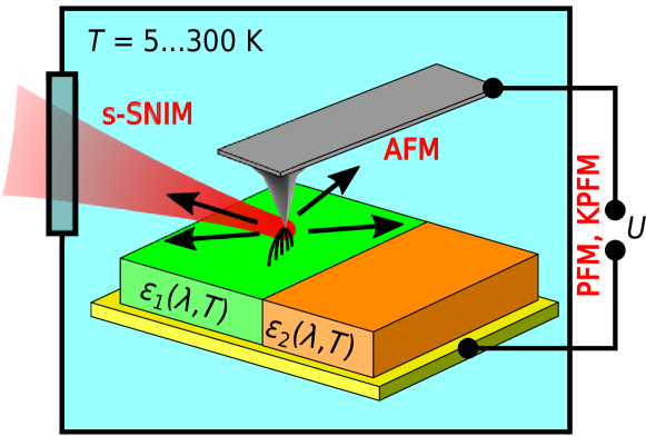
We introduce a scattering-type scanning near-field infrared microscope (s-SNIM) for the local scale near-field sample analysis and spectroscopy from room (RT) down to liquid helium (LHe) temperatures. The extension of s-SNIM down to is in particular crucial for low-temperature phase transitions, e.g. for the examination of superconductors, as well as low energy excitations. The LT s-SNIM performance is tested with CO2-IR excitation at using a bare Au reference and a structured -sample. Furthermore, we quantify the impact of local laser heating under the s-SNIM tip apex by monitoring the light-induced ferroelectric-to-paraelectric phase transition of the skyrmion-hosting multiferroic material GaV4S8 at . We apply LT s-SNIM to study the spectral response of GaV4S8 and its lateral domain structure in the ferroelectric phase by the mid-IR to THz free-electron laser-light source FELBE at the Helmholtz-Zentrum Dresden-Rossendorf, Germany. Notably, our s-SNIM is based on a non-contact atomic force microscope (AFM), and thus can be complemented in-situ by various other AFM techniques, such as topography profiling, piezo-response force microscopy (PFM) and/or Kelvin-probe force microscopy (KPFM). The combination of these methods support the comprehensive study of the mutual interplay in the topographic, electronic and optical properties of surfaces from room temperature down to .
I Introduction
In the last decade, scattering-type scanning near-field infrared optical microscopy (s-SNIM) has developed into a powerful and widespread method for the nanoscale imaging and spectroscopic analysis at infrared (IR) and terahertz (THz) wavelengths Hillenbrand, Taubner, and Keilmann (2002); Huth et al. (2012); Kuschewski et al. (2016); Huber et al. (2016); Amenabar et al. (2017). Providing a resolution ways beyond the classical diffraction limit Knoll and Keilmann (2000), s-SNIM has valuably contributed to the fields of 2D materials (e.g. graphene Ni et al. (2016); Jiang et al. (2016); Alonso-González et al. (2016) and MoS2 Patoka et al. (2016)), to the research of metamaterials and superlenses Taubner et al. (2006); Kehr et al. (2011); Fehrenbacher et al. (2015), as well as to the investigation of semiconductor and organic nanostructures Huth et al. (2012); Westermeier et al. (2014), just to mention a few examples. Nevertheless, a lot of prominent effects in solid-state physics such as superconductivity Ozyuzer et al. (2007); Ahmad et al. (2015), phase transitions in multiferroic materials Döring et al. (2014); McLeod et al. (2016) or the confinement in low-dimensional quantum structures Pajot (2010) need to be explored at low temperatures (LT). Combining LT with the huge potential of IR and THz nanoscopy thus promises great advances in understanding and probing fundamental excitations, such as phonons, magnons and polaritons, in these exotic material classes. The goal of this work is to advertise such a promising combination that involves the “FELBE” tunable free-electron laser (FEL) at the Helmholtz-Zentrum Dresden-Rossendorf, Germany, as a high repetition rate, narrow-band light source tunable from 5 to m wavelength.
To the best of our knowledge, the first work on LT s-SNIM was reported by Moldovan-Doye et al. Moldovan-Doyen et al. (2011) and used the s-SNIM to collect (rather than excite) mid-IR to THz photons with sub-diffraction resolution at , exploring the light emission of an (active) quantum cascade laser element that was coupled to a photonic crystal. Moreover, Yang et al. Yang et al. (2013) demonstrated LT s-SNIM at on non-conducting domains in single crystals that nucleate around topographic defects. Furthermore, a recent publication by McLeod et al. McLeod et al. (2016) impressively showed the detailed mapping of the insulator-to-metal transition at .
Our work here demonstrates LT s-SNIM (Fig. 1) operation down to , while exploring different samples including Au, structured Si-SiO2 and multiferroic with both the CO2 laser and the FEL Kuschewski et al. (2016). The overall LT s-SNIM functionality at various temperatures is illustrated by inspecting a topographically planar Au surface as well as a structured -sample. We study the multiferroic material Milde et al. (2013); Wang et al. (2015); Kézsmárki et al. (2015); Butykai et al. (2017) in order to quantify the local impact of IR radiation by the tip-sample confinement. Moreover the local spectral response as well as the lateral distribution of structural domains below are studied on the same sample by means of in-situ LT s-SNIM, PFM, and KPFM Döring et al. (2014); Döring, Eng, and Kehr (2016); Butykai et al. (2017).
II Setup
II.1 s-SNIM
In s-SNIM, infrared radiation is scattered by the AFM tip that oscillates a few nm above the sample surface. Due to the tip-sample interaction in the optical near-field, the radiation scattered to the far field contains information on the local refractive index tensor of the sample Knoll and Keilmann (2000); Schneider, Grafström, and Eng (2005).
Our LT s-SNIM is based on a custom-made LT atomic force microscope (AFM) system (by Attocube Systems AG) using a Janis Research Company LHe bath cryostat. For s-SNIM measurements, the AFM is operated in tapping-mode Elings et al. (1993), with the cantilever being mechanically excited at its resonance frequency of about with a typical oscillation amplitude of 50 nm. The actual cantilever motion is detected with a fiber-based homodyne interferometer at . We use standard non-contact AFM cantilevers (PPP-NCLPt from NANOSENSORS) for all measurements. AFM tips possess a PtIr5 coating that enables spectrally flat optical excitation over the whole wavelength range from 5 to Rakic et al. (1998). Equally, such tips show an excellent thermal and electrical conductivity, e.g. to allow for specific complementary AFM-mode operation such as PFM or KPFM at one and the same sample position.
PFM makes use of the converse piezoelectric effect, and thus is able to probe different components of the local piezoelectric tensor of the material under inspection Güthner and Dransfeld (1992); Eng et al. (1999); Döring, Eng, and Kehr (2016). Applying a 1 - 10 kHz AC voltage with a typical amplitude of between tip and sample in contact-mode of the AFM leads to local distortions and sample oscillations that are sensed by the AFM probe and demodulated via a lock-in amplifier. The lock-in amplifier measures both amplitude and phase with respect to the excitation. Note that due to the interferometric cantilever detection, only out-of-plane components of the piezoelectric tensor can be addressed in our LT set-up.
KPFM, on the other hand, operates in non-contact mode, and allows to locally quantify and compensate any electrostatic potential offset between tip and sample surface Nonnenmacher, O’Boyle, and Wickramasinghe (1991); Zerweck et al. (2005). KPFM hence not only minimizes cross-talk of electrostatic forces and topography or s-SNIM signals, but equally allows for probing the local work function Shusterman et al. (2007) or sample surface photo-voltage Schumacher et al. (2016) of the sample system simultaneously to s-SNIM investigations. For KPFM, we typically apply a 1 V AC-bias at 4 kHz to the tip on top of the fundamental oscillation amplitude of the cantilever.
II.2 LT s-SNIM optical setup

The optical setup of our s-SNIM is sketched in Fig. 2 (a). As shown, either a narrow-band table-top laser or the FEL at Helmholtz-Zentrum Dresden-Rossendorf are used as IR excitations. The FEL wavelength is tunable over a broad range from to ( to , to or to ), and provides a 1-25 ps pulse train at a repetition rate of 13 MHz. The typical spectral width is about of the actual wavelength. The tunability of the continuous wave (cw) laser is limited to various sharp lines between to .
After passing a geometric beam-splitter (BS), half of the incident radiation is directed to a power meter to monitor the stability of the incident beam at a typical power of to at the position of the LT s-SNIM probe. The other part of the beam is focused onto the tip apex using a Au-coated parabolic mirror sitting outside of the cryostat, with a resulting numerical aperture of about 0.2 and a focus diameter of about at the s-SNIM probe for . Both the incident and the backscattered radiation pass through two cryostat windows: an outer window made of KRS-5, ZnSe or Quartz for different wavelength regimes, respectively, and an inner diamond window. This results in a total attenuation of about for every direction. For all measurements presented here, the radiation is polarized parallel to the incident plane (p-pol) of the tip-sample system, which results in the strongest near-field response Knoll and Keilmann (2000). Nevertheless, it is possible to rotate the polarization by resulting in perpendicular (s-pol) polarization with respect to the incident plane.
The backscattered radiation, that carries the information about the refractive index of the sample on the local scale, is collected by the same parabolic mirror and, after passing through the BS, is focused onto the detector. Depending on the wavelength, we use either a photoconductive mercury cadmium telluride (MCT) detector (), a LHe-cooled gallium doped germanium (Ge:Ga) photoconductive detector (), or a LHe-cooled indium anitmonide (InSb) hot-electron bolometer (). The detector output is demodulated at the -th harmonic of the cantilever resonance frequency using a lock-in amplifier. The resulting signals are further referred to as . This technique effectively suppresses far-field components in the detected signal Knoll and Keilmann (2000); Wurtz, Bachelot, and Royer (1998); Hillenbrand, Stark, and Guckenberger (2000).
II.3 Cryostat
The bath cryostat [see Fig. 2 (b)] consists of two dewar vessels for liquid nitrogen and liquid helium allowing for low-temperature measurements down to . The inner tank connects to the sample tube via a heat exchanger, where the liquid helium cooles the outer wall of the sample tube. The sample tube hosts the AFM and is filled with He gas at a pressure of about in order to facilitate heat transfer between the sample and the wall.
Two thermosensors combined with heating elements are located directly below the sample holder as well as on the wall of the sample tube at the height of the tip. Whenever the temperature at both thermosensors are equal, the system is in a thermal equilibrium, which is the starting point for all LT s-SNIM investigations. The temperature measured at the sample holder is hereafter labeled as , whereas the actual temperature on the sample beneath the tip can differ due to local laser heating as discussed later. The temperature is controlled by the flow of liquid gas and a temperature controller connected to both heating elements.
The optical access to the cryostat is provided in two separate paths: the near-field s-SNIM path (excitation and detection) is coupled in via the parabolic mirror and is focused onto the AFM tip as described above, while the monitoring and adjustment path hosts an optical camera mounted at the rear exit of the cryostat (see Fig. 2).
III Results
III.1 LT s-SNIM perfomance
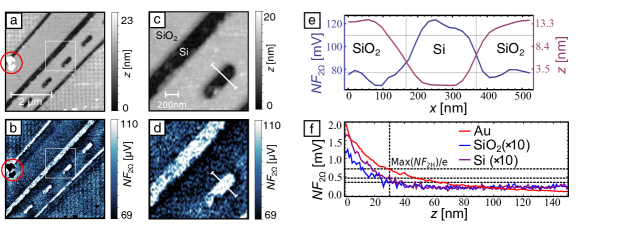
We verify the near-field perfomance of our LT s-SNIM system by probing a structured -sample (for details see Apendix A) at a nominal temperature of using the laser at a wavelength of (see Fig. 3). Note that this sample system has been chosen deliberately to reveal a s-SNIM contrast that is temperature independent and thus can be compared with RT results Kehr et al. (2017).
A topography scan of this sample is depicted in Fig. 3 (a) with a zoomed-in sector (white rectangle) shown in Fig. 3 (c). The higher, bright areas represent whereas the lower, dark areas correspond to Si. The scanned section contains stripes and rectangles of different sizes. Note that the smallest of them are even on the magnitude of the probe’s apex diameter of about . We obtain a RMS-roughness of on , which proves the excellent AFM stability at low temperatures. The corresponding, simultaneously recorded near-field signal [Fig. 3 (b) with zoom (d)] reveals an inverted optical contrast with respect to the topography: Here the areas appear darker than the Si areas. This can be explained by the values of the wavelength-dependent permittivities of both materials taking Chandler-Horowitz and Amirtharaj (2005) and Kischkat et al. (2012) for resulting in lower and higher s-SNIM signals, respectively Knoll and Keilmann (2000). The signal-to-noise ratio of for is approximately 9 and even the smallest structures are clearly visible (top-left and bottom-right areas). Residual particles on the scan, that can neither be assigned to nor to Si, appear dark in the near-field image [see red circle in Fig. 3 (a) and (b)]. This indicates that they are most likely highly insulating and being nonresonant with respect to the excitation wavelength.
A more detailed view is presented in the cross section profile in Fig. 3 (e). The Si- edge in the topography shows a width of less than in the AFM. Notably, the spatial resolution of is similar. To verify the near-field character of , we compare its dependence on the tip-sample distance by retract curves on Si, , and Au, respectively, as depicted in Fig. 3 (f). Both for Si and , NF2Ω is more than 10 times smaller than for the plane Au reference sample since Au, as a metal is highly reflective ( Babar and Weaver (2015)), which results in a huge near-field signal. On all three materials, a non-linear decay of , typical for the near field, is observed within at . This decay is known to scale with the tip diameter Knoll and Keilmann (2000) and therefore is in good agreement with the observed spatial resolution better than .
III.2 Temperature calibration
The sample temperature of our LT s-SNIM system is measured below the sample holder and is thus accurate for samples with excellent thermal conductivity like metals. However, the temperature of the sample at the local position of the tip may be higher due to local heating by the focused IR-laser and additionally due to the field enhancement at the tip apex of the metallic probe. This heating effect is expectedly influenced by sample parameters such as thermal conductivity and wavelength-dependent infrared absorption. Especially the latter will play an important role for the s-SNIM investigation of materials close to absorption resonances, for instance within the Reststrahlenband. Measurements in this regime are of particular interest for s-SNIM since the near-field enhancement conditions result in an enhanced sample sensitivity Hillenbrand, Taubner, and Keilmann (2002); Kehr et al. (2008).
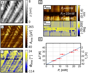
In order to determine experimentally the local sample heating at the tip induced by the infrared laser, the Jahn-Teller transition in multiferroic is used Wang et al. (2015); Butykai et al. (2017). This material becomes ferroelectric below a critical temperature Butykai et al. (2017), which induces a clear contrast in the PFM-signal (see Fig. 4 d) due to ferroelectric domains with polarizations pointing along any of the four -type axes. Fig. 4 (a)-(c) shows topography and PFM images of the (111) surface of a single crystal at , which are all clearly display the lamellar ferroelectric domain pattern. We measure the out-of-plane piezoelectric tensor components discussed in detail by Butykai et al. Butykai et al. (2017).
We study the effect of local heating with a -laser at . Starting with various temperatures the sample is locally heated by the -laser. We monitor the temperature by the two thermosensors of the cryostat starting in thermal equilibrium. Here, a 2D image of PFM amplitude () and PFM phase () of the sample is recorded to obtain the domain pattern and to chose a suitable line with clear domain contrast [Fig. 4 (d)]. During calibration, this line is scanned repeatedly while the laser power is increased gradually until the domains disappear in the PFM-signals at a critical laser power . For the sample is locally heated up to the paraelectric phase, hence the domains vanish leading to zero and random signals. At the transition point, the local temperature due to laser heating reaches . Consequently, the difference is the resulting temperature increase due to power-dependent sample heating. Fig. 4 (d) exemplarily displays such line scans with vanishing domains upon IR illumination. We note that the reappearing domain pattern is probably highly influenced by the ferroelectric boundaries of the heated paraelectric spot. This laser-induced local heating therefore often fully reproduces or strongly correlates with the initial domain structure, depending on the size of the spot heated above the transition temperature. The systematic analysis of controlled heating experiments will be the aim of a future publication. By setting different starting temperatures we find a linear dependence of on for the measured temperature range and extract a laser heating coefficient [see Fig. 4 (e)]. Even though this coefficient depends on material parameters in terms of heat conductivity and absorbance it gives a general estimation of heating effects in our specific LT s-SNIM setup for off-resonant heating far from absorption peaks.
In order to validate the heating coefficient for resonant excitation close to the Reststrahlenband we have applied the same method while operating the FEL around . In this case, is about 10 to 15 % higher as compared to the off-resonant case even though the focus diameter is about 3 times larger than with the CO2 laser at . However, no significant wavelength-dependence could be observed for the resonant case, indicating a major impact of the specific s-SNIM geometry including the metal-coated tip and cantilever on the heating, rather than absorption by the sample.
III.3 Near-field examination of GaV4S8 at
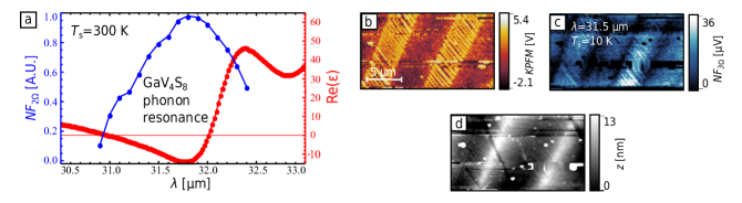
We study the local optical response of the GaV4S8 (111) surface in the ferroelectric phase below the Jahn-Teller transition at . Note that GaV4S8 is optically anisotropic where the optical axes of the different domains are parallel to the -type directions. It has been shown earlier that such anisotropic domains may be probed in resonant s-SNIM Döring et al. (2014); Kehr et al. (2008) at specific wavelengths within the Restrahlenband of the material, making use of the strong IR-active phonon at a wavelength of about or Hlinka et al. (2016); Reschke et al. (2017).
For GaV4S8, such a resonance in the near field occurs at around resulting in an enhanced s-SNIM signal as shown in Fig. 5 (a) for a temperature of . At the same wavelength the permittivity gets negative Reschke et al. (2017) which is crucial for observing a strong resonance in the near-field signal Kehr et al. (2008). Probing the sample surface within the LT- phase, we observe the typical lamella-shaped domain structure Butykai et al. (2017) in all in-situ accessible channels for non-contact AFM, i.e. topography, KPFM, and near-field response [Figs. 5 (b)-(d)]. Considering the laser power of , the temperature calibration discussed above determines the local sample temperature of around within the ferroelectric phase below , which is confirmed by all measured channels, topography, s-SNIM and KPFM.
Please note that we have deliberately chosen here a structure that is known to give the same results for all channels. However, as completely different sample properties are probed with AFM, s-SNIM, and KPFM, namely topography, local infrared-optical response and surface potential, these techniques are complementary and in other types of samples a full comprehensive study is enabled.
IV Conclusion
We have reported here a LT s-SNIM system that, in combination with the FEL as a spectrally narrow, tunable IR laser light source, is capable of operating down to over the broad wavelength range of 5 to 250 . The LT s-SNIM allows for sub-diffraction limited infrared optical examination with a wavelength-independent lateral resolution of about ( at ). We demonstrate LT s-SNIM operation with respect to distance decay on a Au-film, lateral resolution on Si-SiO2 and spectral as well as structural resolution on GaV4S8. Furthermore, we have calibrated the temperature impact due to local laser heating using the Jahn-Teller phase transition of GaV4S8. Moreover, the setup supports complementary AFM techniques such as KPFM and PFM. The combination of these measurement techniques enables far-reaching opportunities for detailed investigations of phase transitions, superconducting materials and quantum structures on the nm length scale.
Acknowledgements.
The authors are greatful to the ELBE team at the Helmholtz-Zentrum Dresden-Rossendorf for the operation of the free-electon laser FELBE and for dedicated support. We thank Stephan Reschke as well as Franz Mayr from the Insitute of Physics, University of Augsburg, Germany for the permittivity data of GaV4S8. The study of GaV4S8 has been conducted within the framework of the Collaborative Research Center ’Correlated Magnetism: From Frustration to Topology’ (SFB 1143) via TP C05. We acknowledge the funding via BMBF Grants Nos. ’05KI0ODB’, ’05KI0BRA’ and ’05K16ODA’ as well as DFG No. ’KE2068/2-1’. The work was supported by the Cluster of Excellence ’Center for Advancing Electronics Dresden (cfaed)’. The work was supported by the joined DAAD project No. ’TKA-DAAD 152294’ and also by the Deutsche Forschungsgemeinschaft(DFG) via the Transregional Research Collaboration TRR 80: From Electronic Correlations to Functionality (Augsburg - Munich - Stuttgart).Appendix A -sample
The structure was first etched into Si covered by a lithographic mask. Subsequently, the trenches were filled with amorphous SiO2 by CVD-growth. After removing the lithography mask, the sample was polished resulting in a structure with only small topography variations between Si and SiO2 and a thickness of the embedded SiO2 of about .
References
- Hillenbrand, Taubner, and Keilmann (2002) R. Hillenbrand, T. Taubner, and F. Keilmann, Nature 418, 159 (2002).
- Huth et al. (2012) F. Huth, A. Govyadinov, S. Amarie, W. Nuansing, F. Keilmann, and R. Hillenbrand, Nano Lett. 12, 3973 (2012).
- Kuschewski et al. (2016) F. Kuschewski, H.-G. von Ribbeck, J. Döring, S. Winnerl, L. M. Eng, and S. C. Kehr, Appl. Phys. Lett. 108, 113102 (2016).
- Huber et al. (2016) M. A. Huber, F. Mooshammer, M. Plankl, L. Viti, F. Sandner, L. Z. Kastner, T. Frank, J. Fabian, M. S. Vitiello, T. L. Cocker, and R. Huber, Nat. Nanotechnol. 12, 207 (2016).
- Amenabar et al. (2017) I. Amenabar, S. Poly, M. Goikoetxea, W. Nuansing, P. Lasch, and R. Hillenbrand, Nat. Commun. 8, 14402 (2017).
- Knoll and Keilmann (2000) B. Knoll and F. Keilmann, Opt. Commun. 182, 321 (2000).
- Ni et al. (2016) G. X. Ni, L. Wang, M. D. Goldflam, M. Wagner, Z. Fei, A. S. McLeod, M. K. Liu, F. Keilmann, B. Özyilmaz, A. H. Castro Neto, J. Hone, M. M. Fogler, and D. N. Basov, Nat. Photonics 10, 244 (2016).
- Jiang et al. (2016) L. Jiang, Z. Shi, B. Zeng, S. Wang, J.-H. Kang, T. Joshi, C. Jin, L. Ju, J. Kim, T. Lyu, Y.-R. Shen, M. Crommie, H.-J. Gao, and F. Wang, Nat. Mater. 15, 1 (2016).
- Alonso-González et al. (2016) P. Alonso-González, A. Y. Nikitin, Y. Gao, A. Woessner, M. B. Lundeberg, A. Principi, N. Forcellini, W. Yan, S. Vélez, A. J. Huber, K. Watanabe, T. Taniguchi, F. Casanova, L. E. Hueso, M. Polini, J. Hone, F. H. L. Koppens, and R. Hillenbrand, Nat. Nanotechnol. 12, 1 (2016).
- Patoka et al. (2016) P. Patoka, G. Ulrich, A. E. Nguyen, L. Bartels, P. A. Dowben, V. Turkowski, T. S. Rahman, P. Hermann, B. Kastner, A. Hoehl, G. Ulm, and E. Ruhl, Opt. Express 24, 1154 (2016).
- Taubner et al. (2006) T. Taubner, D. Korobkin, Y. Urzhumov, G. Shvets, and R. Hillenbrand, Science 313, 1595 (2006).
- Kehr et al. (2011) S. C. Kehr, Y. M. Liu, L. W. Martin, P. Yu, M. Gajek, S.-Y. Yang, C.-H. Yang, M. T. Wenzel, R. Jacob, H.-G. von Ribbeck, M. Helm, X. Zhang, L. M. Eng, and R. Ramesh, Nat. Commun. 2, 249 (2011).
- Fehrenbacher et al. (2015) M. Fehrenbacher, S. Winnerl, H. Schneider, J. Döring, S. C. Kehr, L. M. Eng, Y. Huo, O. G. Schmidt, K. Yao, Y. Liu, and M. Helm, Nano Lett. 15, 1057 (2015).
- Westermeier et al. (2014) C. Westermeier, A. Cernescu, S. Amarie, C. Liewald, F. Keilmann, and B. Nickel, Nat. Commun. 5, 4101 (2014).
- Ozyuzer et al. (2007) L. Ozyuzer, a. E. Koshelev, C. Kurter, N. Gopalsami, Q. Li, M. Tachiki, K. Kadowaki, T. Yamamoto, H. Minami, H. Yamaguchi, T. Tachiki, K. E. Gray, W.-K. Kwok, and U. Welp, Science 318, 1291 (2007).
- Ahmad et al. (2015) D. Ahmad, B. H. Min, Y. I. Seo, W. J. Choi, S.-I. Kimura, J. Seo, and Y. S. Kwon, Supercond. Sci. Technol. 28, 075002 (2015).
- Döring et al. (2014) J. Döring, H.-G. non Ribbeck, M. Fehrenbacher, S. C. Kehr, and L. M. Eng, Appl. Phys. Lett. 105, 053109 (2014).
- McLeod et al. (2016) A. S. McLeod, E. van Heumen, J. G. Ramirez, S. Wang, T. Saerbeck, S. Guenon, M. Goldflam, L. Anderegg, P. Kelly, A. Mueller, M. K. Liu, I. K. Schuller, and D. N. Basov, Nat. Phys. 13, 80 (2016).
- Pajot (2010) B. Pajot, Optical Absorption of Impurities and Defects in Semiconducting Crystals, Springer Series in Solid-State Sciences, Vol. 158 (Springer Berlin Heidelberg, Berlin, Heidelberg, 2010).
- Moldovan-Doyen et al. (2011) I. C. Moldovan-Doyen, G. Xu, L. Greusard, G. Sevin, E. Strupiechonski, G. Beaudoin, I. Sagnes, S. P. Khanna, E. H. Linfield, A. G. Davies, R. Colombelli, and Y. De Wilde, Appl. Phys. Lett. 98, 231112 (2011).
- Yang et al. (2013) H. U. Yang, E. Hebestreit, E. E. Josberger, and M. B. Raschke, Rev. Sci. Instrum. 84, 023701 (2013).
- Milde et al. (2013) P. Milde, D. Köhler, J. Seidel, L. M. Eng, A. Bauer, A. Chacon, J. Kindervater, S. Mühlbauer, C. Pfleiderer, S. Buhrandt, C. Schütte, and A. Rosch, Science 340, 1076 (2013).
- Wang et al. (2015) Z. Wang, E. Ruff, M. Schmidt, V. Tsurkan, I. Kézsmárki, P. Lunkenheimer, and A. Loidl, Phys. Rev. Lett. 115, 1 (2015).
- Kézsmárki et al. (2015) I. Kézsmárki, S. Bordács, P. Milde, E. Neuber, L. M. Eng, J. S. White, H. M. Rønnow, C. D. Dewhurst, M. Mochizuki, K. Yanai, H. Nakamura, D. Ehlers, V. Tsurkan, and A. Loidl, Nat. Mater. 14, 1116 (2015).
- Butykai et al. (2017) Á. Butykai, S. Bordács, I. Kézsmárki, V. Tsurkan, A. Loidl, J. Döring, P. Milde, S. C. Kehr, and L. M. Eng, Sci. Rep. 7, 44663 (2017).
- Döring, Eng, and Kehr (2016) J. Döring, L. M. Eng, and S. C. Kehr, J. Appl. Phys. 120 (2016).
- Schneider, Grafström, and Eng (2005) S. C. Schneider, S. Grafström, and L. M. Eng, Phys. Rev. B - Condens. Matter Mater. Phys. 71, 115418 (2005).
- Elings et al. (1993) V. B. Elings, Z. Q., I. D., K. K., Q. Zhong, D. Inniss, K. Kjoller, and V. Elings, Surf. Sci. Lett. 290, 688 (1993).
- Rakic et al. (1998) A. D. Rakic, A. B. Djurisic, J. M. Elazar, and M. L. Majewski, Appl. Opt. 37, 5271 (1998).
- Güthner and Dransfeld (1992) P. Güthner and K. Dransfeld, Appl. Phys. Lett. 61, 1137 (1992).
- Eng et al. (1999) L. M. Eng, H.-J. Güntherodt, G. A. Schneider, U. Köpke, and J. Muñoz Saldaña, Appl. Phys. Lett. 74, 233 (1999).
- Nonnenmacher, O’Boyle, and Wickramasinghe (1991) M. Nonnenmacher, M. P. O’Boyle, and H. K. Wickramasinghe, Appl. Phys. Lett. 58, 2921 (1991).
- Zerweck et al. (2005) U. Zerweck, C. Loppacher, T. Otto, S. Grafström, and L. M. Eng, Phys. Rev. B - Condens. Matter Mater. Phys. 71, 1 (2005).
- Shusterman et al. (2007) S. Shusterman, A. Raizman, A. Sher, Y. Parltiel, A. Schwarzman, E. Lepkifker, and Y. Rosenwaks, Nano Lett. 7, 2089 (2007).
- Schumacher et al. (2016) Z. Schumacher, Y. Miyahara, A. Spielhofer, and P. Grutter, Phys. Rev. Appl. 5, 1 (2016).
- Wurtz, Bachelot, and Royer (1998) G. Wurtz, R. Bachelot, and P. Royer, Rev. Sci. Instrum. 69, 1735 (1998).
- Hillenbrand, Stark, and Guckenberger (2000) R. Hillenbrand, M. Stark, and R. Guckenberger, Appl. Phys. Lett. 76, 3478 (2000).
- Kehr et al. (2017) S. C. Kehr, J. Döring, M. Gensch, M. Helm, and L. M. Eng, Synchrotron Radiat. News 30, 31 (2017).
- Chandler-Horowitz and Amirtharaj (2005) D. Chandler-Horowitz and P. M. Amirtharaj, J. Appl. Phys. 97, 123526 (2005).
- Kischkat et al. (2012) J. Kischkat, S. Peters, B. Gruska, M. Semtsiv, M. Chashnikova, M. Klinkmüller, O. Fedosenko, S. Machulik, A. Aleksandrova, G. Monastyrskyi, Y. Flores, and W. T. Masselink, Appl. Opt. 51, 6789 (2012).
- Babar and Weaver (2015) S. Babar and J. H. Weaver, Appl. Opt. 54, 477 (2015).
- Kehr et al. (2008) S. C. Kehr, M. Cebula, O. Mieth, T. Härtling, J. Seidel, S. Grafström, L. M. Eng, S. Winnerl, D. Stehr, and M. Helm, Phys. Rev. Lett. 100, 1 (2008).
- Reschke et al. (2017) S. Reschke, F. Mayr, Z. Wang, P. Lunkenheimer, W. Li, D. Szaller, S. Bordács, I. Kézsmárki, V. Tsurkan, and A. Loidl, ArXiv e-prints , 1 (2017), arXiv:1704.08602 .
- Hlinka et al. (2016) J. Hlinka, F. Borodavka, I. Rafalovskyi, Z. Docekalova, J. Pokorny, I. Gregora, V. Tsurkan, H. Nakamura, F. Mayr, C. A. Kuntscher, A. Loidl, S. Bordács, D. Szaller, H. J. Lee, J. H. Lee, and I. Kézsmárki, Phys. Rev. B 94, 1 (2016).