Accelerator Codesign as Non-Linear Optimization
Abstract
We propose an optimization approach for determining both hardware and software parameters for the efficient implementation of a (family of) applications called dense stencil computations on programmable GPGPUs. We first introduce a simple, analytical model for the silicon area usage of accelerator architectures and a workload characterization of stencil computations. We combine this characterization with a parametric execution time model and formulate a mathematical optimization problem. That problem seeks to maximize a common objective function of all the hardware and software parameters. The solution to this problem therefore “solves” the codesign problem: simultaneously choosing software-hardware parameters to optimize total performance.
We validate this approach by proposing architectural variants of the NVIDIA Maxwell GTX-980 (respectively, Titan X) specifically tuned to a predetermined workload of four common 2D stencils (Heat, Jacobi, Laplacian, and Gradient) and two 3D ones (Heat and Laplacian). Our model predicts that performance would potentially improve by 28% (respectively, 33%) with simple tweaks to the hardware parameters such as adapting coarse and fine-grained parallelism by changing the number of streaming multiprocessors and the number of compute cores each contains. We propose a set of Pareto-optimal design points to exploit the trade-off between performance and silicon area and show that by additionally eliminating GPU caches, we can get a further 2-fold improvement.
I Introduction
Software-hardware codesign is one of the proposed enabling technologies for exascale computing and beyond [31]. Currently, hardware and software design are done largely separately. Hardware manufacturers design and produce a high-performance computing (HPC) system with great computing potential and deliver it to customers, who then try to adapt their application codes to run on the new system. But because of a typically occurring mismatch between hardware and software structure and parameters, such codes are often only able to run at a small fraction of the total performance the new hardware can reach. Hence, optimizing both the hardware and software parameters simultaneously during hardware design is considered as a promising way to achieve better hardware usage efficiency and thereby enabling leadership-class HPC availability at a more manageable cost and energy efficiency.
The design of HPC systems and supercomputers is by no means the only scenario where such optimization problems occur. The execution platforms of typical consumer devices like smart phones and tablets consist of very heterogeneous Multi-Processor Systems-on-Chip (MPSoCs) and the design challenges for them are similar.
Despite the appeal of an approach to simultaneously optimize for software and hardware, its implementation represents a formidable challenge because of the huge search space. Previous approaches [7, 9, 22], pick a hardware model from the hardware design space, a software model from the software design space, map onto , estimate the performance of the mapping, and iterate until a desirable quality is achieved. But not only each of the software and hardware design spaces can be huge, each iteration takes a long time since finding a good mapping of onto and estimating the performance of the resulting implementation are themselves challenging computational problems.
In this paper, we propose a new approach for the software-hardware codesign problem that avoids these pitfalls by considerably shrinking the design space and making its exploration possible by formulating the optimization problem in a way that allows the use of existing powerful optimization solvers. We apply the methodology to programmable accelerators: Graphics Processing Units (GPUs), and for stencil codes. The key elements of our approach are to exploit multiple forms of domain-specificity. Our main contributions are:
-
•
We propose a new approach (see Section II) to software-hardware codesign that it is computationally feasible and provides interesting insights.
-
•
We develop a simple, analytical model for the silicon area (Section III) of programmable accelerator architectures, and calibrate it using the NVIDIA Maxwell class GPUs.
- •
-
•
Our analysis (Section V) provides interesting insights. We produce a set of Pareto optimal designs that represent the optimal combination of hardware and compiler parameters. They allow for up to improvement in performance as measured in GFLOPs/sec.
II Approach
The key element of our approach is exploiting domain specificity. We do this in three ways. First, we tackle a specific (family of) computations that are nevertheless very important in many embedded systems. This class of computations, called dense stencils, includes the compute intensive parts of many image processing kernels, simulation of physical systems relevant to realistic visualization, as well as the solution of partial differential equations (PDEs) that arise in many cyber-physical systems such as automobile control and avionics.
Second, we target GPU-like vector-parallel programmable accelerators. Such components are now becoming de-facto standard in most embedded platforms and MPSoCs since they provide lightweight parallelism and energy/power efficiency. We further argue that they will become ubiquitous for the following reasons. Any device on the market today that has a screen (essentially, any device, period) has to render images. GPUs are natural platforms for this processing (for speed and efficiency). So all systems will have an accelerator, by default. If the system now needs any additional dense stencil computations, the natural target for performing it in the most speed/power/energy efficient manner is on the accelerator.
The third element of domain specificity is that we exploit a formalism called the polyhedral model as the tool to map dense stencil computations to GPU accelerators. Developed over the past thirty years [30, 29, 12, 13, 14], it has matured into a powerful technology, now incorporated into gcc, llvm and in commercial compilers [Rstream, IBM]. Tools targeting GPUs are also available [16, 3]. We recently showed [27] that these elements of the domain specificity can be combined to develop a simple analytical model for the execution time of tiled stencil codes on GPUs, and that this model can be used to solve for optimal tile size selection.
Thus, we formulate the domain specific optimization problem as: simultaneously optimize compilation and hardware/architectural parameters for compiling stencil computations to GPU-like vector-parallel accelerators.
To explain our overall approach, first recall how tile size selection is formulated as an optimization problem [27]. A given class of programs, with some problem parameters, (e.g., size of the iteration space, number of array variables) is compiled to an accelerator with some hardware parameters (e.g., number of cores, number of vector units, cache size, etc.) The compiler itself may use some well defined optimization strategies (e.g., tiling, skewing, parallelization, etc.), and may have some software parameters, notably tile sizes ().
We develop an analytical function, that predicts the execution time of the target program as a function of these parameters. The values of the parameters must satisfy a set of feasibility constraints (e.g., tile sizes must be such that the data footprint of a tile must fit in the available scratchpad memory) denoted by . Then, optimal tile size selection is simply solving the following problem:
| (1) | ||||
| subject to: |
Here, the unknown variables are . The hardware and program parameters are considered as constants—compiling a different program and/or compiling to a different target machine entails solving a new optimization problem. Extending this to codesign requires the following steps.
-
•
Workload characterization We first pick a set of representative program instances. For each one, we use profiling to pick the probability/frequency with which it occurs in the workload. Each program may be executed with a range of program parameters, and we also have a frequency with which of these appear in the workload. So, are the program parameters of the -th instance of the -th benchmark, and the set is , the range of program parameters.
-
•
Codesign Optimization Now we formulate a simple extension of (2). Instead of leaving the hardware parameters as constants, we allow them to be unknown variables of the optimization problem, which now becomes
(2) subject to: -
•
Area Model Since is now an unknown, we must formulate its feasible space, precisely. For this, we develop an analytical model of the area of the accelerator. We assume that we are given an area budget within which the accelerator must fit, and solve the optimization problems over the resulting feasible space.
This seems (deceptively) simple, but the devil is in the detail. The resulting optimization problem has many hundreds of variables, and has non-convex constraints and objective functions, making it computationally intractable. The details of how we solve it are explained in Section IV.
III Area Model
We now develop an analytic model for the total silicon area of a GPU accelerator. We faced some difficulties in deriving an acceptable analytical model, as silicon data had to be reverse engineered from extremely limited public domain resources. As a general observation, within each GPU family, there is little diversity in the parameter configurations. For the Maxwell family of GPUs, the GTX980 and Titan X chips were chosen as two sufficiently distinct points to calibrate our analytical models. The calibration itself was performed by evaluating die photomicrographs, publicly available information about the nVidia GTX-980 (Maxwell series) GPU, and other generally accepted memory architecture models. The model validation was done by comparing the predictions with known data on the Maxwell series Titan X GPU. We found the model prediction to be accurate to within, 2%, though this number is not significant.111Although a many configurations of any family of GPUs are spaced out, they come from binning only a small number of distinct dies. We ended up calibrating our model on one die and validating it on only another one.
III-A Analytical Model for GPU Area
The area model is a function of the main parameters that we want to select optimally in the codesign problem: the number of SMs, , the number of vector units or cores in each SM, , and the respective sizes of the register file and shared memory size of the SM, , and . Table I shows a summary of the various parameters used in developing the area model.
| Name | Description |
|---|---|
| overhead area per kB of register-memory per vector-unit | |
| overhead area per kB of shared-memory per SM | |
| L1 cache overhead area per SM-pair | |
| L2 cache overhead area | |
| common overhead area (I/O, global routing etc) per SM | |
| area per register-file-bank per kB per vector-unit | |
| area per shared-memory-bank per kB per SM | |
| L1 cache area per kB per SM-pair | |
| L2 cache area per kB | |
| core-logic area within a vector-unit | |
| total number of SM on the GPU chip | |
| number of vector-units per SM | |
| kB of register files per vector-unit | |
| kB of shared memory per SM | |
| kB of L1 cache per SM-pair | |
| kB of L2 cache | |
| total GPU chip die area | |
| total shared-memory die area | |
| total cache die area | |
| total on-chip overhead die area | |
| total load-store unit die area | |
| total special-function unit die area | |
| total fetch-decode unit die area | |
| total instruction-cache die area | |
| load-store unit die area per SM | |
| load-store unit die area per vector-unit | |
| memory die area per SM | |
| special-function unit die area per vector-unit |
| (3) |
where is the cost of each SM, is the total area of the on-chip L1 and L2 caches, and is the overall overhead area cost. The term accounts for several components which are of only peripheral interest to us, such as metal-layer routing overheads, I/O pads, buffers, and clock-signal global distribution trees, gigathread scheduler, PCI express interface, raster engine, and memory controller. Based on our current understanding of the nVidia architecture, a best effort annotation of various functional blocks is shown overlaid on a die photomicrograph of GTX980 chip in Figure 1. The term denotes the area of a single SM, and we develop it next. The following micro-architectural elements comprise an SM:
-
•
Individual vector units: The area cost of this is .
-
•
Load-store unit (LSUs): Every core may issue independent memory requests, to either the shared memory or to global memory. Therefore the LSU has a component that is replicated per core, and also a shared component that (eventually) collects together all requests from a single warp and interfaces to the (global) memory hierarchy. Therefore .
-
•
Special function units (SFUs): These are dedicated functional units that are used for common graphics functions, transcendentals, etc. Their number is not always exactly equal to , (e.g., in the nVidia GTX-980, there is one SFU every 8 cores) but we model it as a linear function of , i.e., .
-
•
Instruction fetch-decode unit (FDU): Like the I-cache, there is a single FDU per SM, so its cost is simply a constant
-
•
Various specialized “memories:” the shared memory used as scratchpad, the register file, the instruction cache, the texture and other special caches. We call this term and develop it separately.
Of these, the memories other than register files and the FDU are shared by the entire SM, while the register files, SFU and LSU are accounted for on a per vector unit basis. Hence,
| (4) |
where , and depends on the capacity of each of the individual memories. Of these, we are interested in modeling the area costs for the register file, shared (scratchpad) memory, L1 cache and L2 cache; so the others are treated as constants absorbed in . L1 cache is shared by a pair of SM units, while the L2 cache is shared by all the SM units on the chip. The register files are organized so that a few registers (512 registers each 32 bits wide in GTX980) are exclusively accessible by each vector-unit. The shared memory is accessible by all vector-units in an SM. Assuming independent linear cost models for each of these four memory types, therefore, . Here, we have subscribed to a design philosophy where the size of the L2 cache is not proportional to the number of SM units, it is a constant. This choice seems to be the norm, in that the GTX980 chip with SMs has an L2 cache of MB, whereas the Titan X with 24 SMs has an L2 cache of MB. Another design choice we make is the following – the common area overhead , comprising the I/O pads, buffers, routing, gigathread engine, PCI and memory controllers, is also assumed to be proportional to the number of SMs222This design choice is by no means the only possible one – another possibility is to also have an additional constant term, though one would need more than two GPUs in the Maxwell family with different die areas to calibrate such a model., that is, . Substituting this result in the above equations, collecting all common overhead area contributions including into , and further simplifying, we get,
| (5) |
III-B Calibrating the Model
Since the overall area model involves non-linear terms, we used an incremental fitting approach to calibrate our model. We first developed linear regression models for the area contribution due to the memory elements. We then incorporated the memory element area model into a measurement based linear model for the area due to the SM core vector units.
The Maxwell family was fabricated using the TSMC nm process. For this process, the typical SRAM bit cell has an area of only to [20]. The total area used by memory banks, be it the register files, shared memory, or the caches, involve the much more substantial additional area used for routing, addressing, read, write and bit-sense amplification logic. The register file, shared memory, and cache area models should take this overhead into account, by accounting for the bit width, number of addresses, and number of read and write ports. We used the open source Cacti 6.5 RAM and cache estimation tool from HP labs [19] to optimize and calibrate all our memory models:
-
•
Register files: We modeled the register file at the vector-unit level with a data bus of bits. For example, the GTX980 chip has 512 such registers per vector-unit. For configuring the register file in Cacti, we assumed a ‘ram’ model which is direct-mapped, with exclusive single ended read ports and exclusive write port per vector-unit. Our Cacti design objective was to aggressively minimize area, as register files are placed physically close to the logic core where space is at an extra premium.
-
•
Shared memory units: The shared memory bank is organized per SM. The GTX980 chip has kB of shared memory per SM. The user is allowed to optionally dynamically configure a part of the shared memory in an SM as cache. We assumed, for the purpose of Cacti tool configuration, that it is a direct mapped ‘ram’ type memory with bit wide data bus, on each of its read-write ports per SM. Our design objective was to minimize area, with a secondary objective of minimizing propagation delays.
-
•
L1 cache: The L1 cache is shared by two adjacent SM units. The GTX980 has kB of L1 cache per SM. Our Cacti model for L1 cache is a ‘cache’ type memory with a line-size of bytes, and a data width of bits. We also chose a conservative setting of full associativity for this cache level. There are exclusive read ports for downstream access from the logic cores, and exclusive write ports for upstream access from the L2 cache. The design was tailored for speed and the optimization objective was primarily propagation delay and secondarily power dissipation.
-
•
L2 cache: For the nVidia Maxwell architecture, the L2 cache is shared by all the SM units on the chip. For this GPU family, the L2 cache is on average kB per SM. Our Cacti configuration assumes a ‘cache’ type memory with a line-size of bytes, and a data width of bits on each of its exclusive read ports feeding into every L1 cache on the chip downstream. There is also a exclusive read-write port for upstream interface with the memory controllers. The design objective was a weighted mix of delay and area.
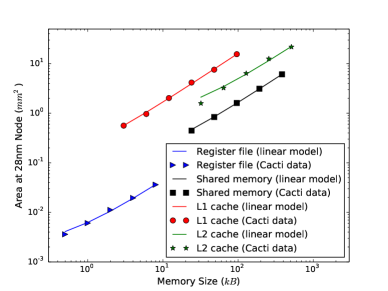
Using these Cacti models, we obtained area estimates for per vector-unit register file banks of , and bytes each. We then derived a linear fit model for the area given the bank size. The coefficients of this model were and .
Similarly, we obtained area estimates for per SM shared memory banks of , and kilo-bytes size each, and derived a linear fit model. The coefficients of this linear model were and .
The L1 and L2 cache models were similarly calibrated by performing optimizations using our Cacti models as described earlier. The L1 linear fit model was obtained with per SM-pair sizes of , and kilo-bytes each. The model parameters obtained were and . The L2 linear fit model was obtained with per SM sizes of , and kilo-bytes each. The parameters obtained were and . The linear regression models obtained as above are shown in Figure 2.
nVidia publishes obfuscated die-shots of their GPU chips, though these photographs are sometimes not to scale. The community of GPU enthusiasts and researchers have also attempted to decap packaged GPU chips and photograph the silicon dies independently. For example, Fritzchens Fritz [15] has a vast collection of nVidia die photographs which we have used in association with the obfuscated die shots published by nVidia. The nVidia official “die-shots” tend to show demarcated logical functional blocks - for SMs, this includes not only the SM core logic regions, but also the associated control, and thread-scheduler logic areas too. We have factored these aspects into account while making our area measurements. The area measurements were initially made in terms of pixels, and later normalized to using the total die area from the GPU’s datasheet. As a verification of the memory area model calibration, we first measured the area of the following memory blocks on the die photograph – L2: , L1: , and shared memory: . These measured areas matched quite well with the linear model predictions – L2: , L1: , and shared memory: . Furthermore, from the die photomicrographs for GTX980 [15, 25], area per vector-unit logic core was measured to be , excluding the register-file area. Similarly, measurements on GTX980 die photograph gave an area estimate of for the overhead region containing the I/O pads, buffers, memory controllers, gigathread and raster engines and PCI controller, which gives an per SM. The total published die area for GTX980 is also known to be . For the Maxwell family, our overall area model is therefore given by:
| (6) |
III-C Validating the Model
In order to validate our area model, we applied it to another member of the Maxwell family, the Titan X for which the total die area is known. Our model predicts a total area of which is within an error of of the published die area of .
Our area model above is only valid for the functional blocks as implemented for the specific TSMC -nm process used to fabricate the nVidia Maxwell chips. The newer Pascal family of nVidia GPUs are fabricated on a -nm technology node. If each of the constituent functional block’s chip level layouts were to remain same across technology nodes, and were only optically reduced down by a certain shrinkage factor, then the area model can be similarly rescaled and reused. However, the shift from -nm to -nm involves a non-trivial move from planar CMOS to 3D-FINFET technology, and consequently a simple area rescaling would clearly not be sufficient to predict the area parameters of Pascal family chips. However the overall methodology still remains applicable to any technology node or device family.
IV Optimizing software and hardware parameters
We now show how to use the analytical chip area model and our previous execution time model [27] to formulate and solve an optimization problem for simultaneously finding optimal hardware and software parameters.
IV-A Problem formulation
The parameters we are going to optimize are the elementary software (ES) parameters , , and and the elementary hardware (EH) parameters , , and . For each combination of EH parameters, the corresponding running time in the objective function will be defined as the optimal time for that hardware configuration and for the stencil of interest over all possible choices of tile sizes.
This results in the following optimization problem, which finds the best EH parameters for a given stencil and a given bound on the chip area denoted by
| (7) | ||||
| subject to: | (8) | |||
| (9) | ||||
| (10) | ||||
| (11) | ||||
| (12) | ||||
| (13) | ||||
| (14) | ||||
| (15) |
Note that in (7) is in fact a function not only of the parameters , , , , , and , but also of the other parameters detailed elsewhere [27]. Also, for 3D stencils there is an additional parameter to function (7) which is the tile size in the third space dimension . We are only explicitly using those parameters that are needed in the specific context. Constraint (8) guarantees that the total area for the current hardware configuration, according to the area model, does not exceed the optimization parameter chip_area. Constraint (9) asks the memory required for each tile not to exceed , the shared memory available for a threadblock, while (10) and (11) restricts the number of tiles simultaneously executed by an SM (using hyperthreading) to be no greater than the max threadblocks an SM can handle and such that the total memory of all such tiles is at most . The values of and can be only integers, and , , , and should be multiples of 32, 32k, and 2, respectively, by constraints (11)–(15). We require to be even, to be multiple of 32, and to be multiple of 32k in order to be consistent with the patterns for these parameters chosen by the manufacturers in existing GPUs. For the tile sizes, we want to be even as it is a requirement for hybrid-hexagonal tiling [16], while being a multiple of 32 ensures that neighboring threads in dimension can fit in a number of full warps, where each warp is a group of 32 threads.
The optimization problem (7)–(15) allows, given a stencil of interest (say Jacobi 2D) and specific values of the problem size parameters and , to find a combination of software and hardware parameters that results in optimal (smallest) run time. However, it is unlikely that one may need a hardware that will be used for just a single problem size. A more relevant problem is to optimize the hardware over a set of problem sizes. Given a set of sizes and a frequency function such that is the expected frequency the size will be encountered for the intended application, the corresponding new objective becomes
| (16) |
where is the set of tile sizes, with each tile size given as a triple , and ( is for Jacobi) is the time-model function, whose EH parameters are , , , and whose ES parameters are . Hence, the optimization problem (16) has decision variables.
In our experiments, we use as values for the set and for the set and define . We use since it is known from practice that no more than iterations are needed for convergence. One can check that and hence the number of variables for problem (16) is . While this is a small number of variables for optimization problems with a nice structure, e.g., linear or convex, in our case the problem is of a difficult type, with all variables being integer and the objective function and the constraints being rational functions. Because of the floor and ceiling functions used in our time model, our objective and constraints are not even continuous, although this can be handled by introducing one new integer variable per floor or ceiling function. This however further increases the number of variables, which becomes .
Regardless of the fact that an optimization problem with 162 integer variables and non-convex constraints and objective is in most cases computationally infeasible, we will consider an even larger version of (16), and then show how both problems can be simplified and solved accurately and in reasonable time by exploring the separability of the objective.
Let us first describe a problem setting that is more relevant from practical point of view. While (16) can be used to determine stencil-optimal architecture parameters, in many cases, people would be interested in having a special-purpose hardware that is optimized for an application whose computation time is dominated by a set of often-used kernels. In our case, we assume that a hypothetical application is using the six stencils studied in this paper and by studying a profiling data we have determined how often each stencil is used and a distribution of problem dimension sizes for each application. In our experiments we use four 2D stencils: Jacobi-2D, Heat-2D, Laplacian-2D, and Gradient-2D, all first order stencils, and two 3D stencils: Heat-3D and Laplacian-3D. All 2D stencils have two space dimensions and one time dimension, while the 3D stencils have three space dimensions and one time dimension. We then extend the definition of the frequency function so that, for each code , denotes the frequency of using in application . Moreover, given and , let denote the frequency with which problem size has been used for stencil . Then the updated objective of the resulting optimization problem becomes
| (17) |
The set here includes tile sizes for each and each . Hence the number of integer variables for problem (17) is , which is too large to be solved by existing solvers, given that the problem is nonlinear, nonconvex, and with integer variables. Fortunately, the problem can be made feasible by dividing the variables into two sets and combining exhaustive search on the first set with nonlinear programming optimization on the second.
IV-B Solving the optimization problem
The main observation that helps us solve problem (17) more efficiently is the fact that, if we knew the optimal value of parameters , then the objective (17) would become separable since can be minimized with respect to the tile sizes independently for each and . Formally, we are transforming (17) into the following equivalent problem
| (18) |
Since we don’t know , then we replace in (18) with all feasible values of and, for each such value, we run a separate optimization problem with respect to for each combination of and . As a result, instead of solving one large problem (17) with 642 variables, we do exhaustive search on the space and, for each point in that space, we solve using a nonlinear solver an optimization problem with only 10 integer variables. (While the variables we are interested in are only three, the optimization problem includes additional internal variables such as the optimal number of tiles for hyperthreading and variables used to simplify some nonlinearities, resulting in total number of 10.)
To further reduce the number of these problems, we will fix the range of values of the parameters as follows: and is even, and is a multiple of 32, which come from the constraints of (7)–(15). with the requirement (14) to be multiple of 48k and positive. In addition, we explore the sizes , and for .
We ran three experiments using chip areas in the range . Since we haven’t tied the experiments to a specific application, we assumed all six stencils equally likely, and that each size combination also equally likely; i.e., we set all coefficients in (17) to 1. For solving the optimization problems we used the open source solver bonmin [1]. The average solution time per optimization instance is 19 sec (although it varies a lot from instance to instance), so the total solution time varies between 7 and 24 hours depending on the chip area. Also note that, in the execution time model we use a parameter , the execution time of a single iteration on one thread. For optimal tile size selection, we measured this parameter for the different stencils. Although there was a small difference between the two platforms (GTX-980 and Titan X) we used the former value for our experiments.
V Discussion and Perspectives
We will now illustrate how our codesign optimization can be used to explore various scenarios. Furthermore, we will see that the trick of partitioning the design space into a number of independent optimization problems, described by Eqn. (18), has added advantages of enabling investigation of a number of scenarios without re-solving optimization problems.
V-A Design Space Exploration
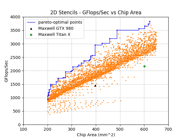
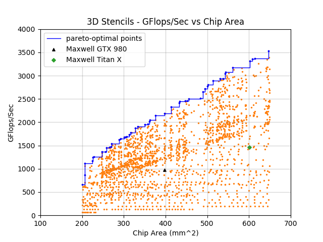
Given a range of area budgets between 200 and 650 , we enumerated all feasible architecture, and solved the codesign optimization problem for each one. We separated the workload into two classes, 2D stencils and 3D stencils. Each one illustrates interesting features. For each class, we assumed a uniform frequency (each instance is equally likely, and within each instance, each problem size is also equally likely). Figure 3 shows out results. The first observation is that only about 1% of the thousands of feasible hardware designs (the Pareto optimal designs shown in blue) are worth exploring further, leading to a significant pruning of the design space.
We also show in the same figure the performance of two standard design points, Nvidia’s GTX980 and TitanX architectures. For comparable area, we can improve performance by 104% (resp., 69% wrt. TitanX) for 2D stencils, and by 123% (resp., 126%) for 3D stencils. A large part of the gains come from the fact that our proposed designs do not have caches because the HHC compiler for which our model is specialized [16] generates codes to perform data transfers explicitly rather than relying on caches. To compensate for this, we could “delete” the caches from the GTX980 and TitanX, which reduces their areas to respectively, and . The performance of the corresponding Pareto optimal designs for those reduced areas is 9.34% (resp., 28.44% for the cache-less TitanX) better for 2D stencils and 9.22% (resp., 33.15%) better for 3D stencils.
V-B Workload Sensitivity
Eqn. (18) partitions the design space into a number of independent optimization problems. This allows us to explore other hypothetical scenarios “for free.” As an example, changing frequencies of the different programs in the benchmark suite requires us to simply recompute new weighted sums of optimal values of minimization problems that we have already solved. A specific example would be to hypothetically set the frequency for one of the benchmarks as one (and zero for the others) thereby allowing us to explore designs optimized for a single kernel. It also helps determine whether the chosen suite is representative of the mix that occurs in practice. Table II illustrates the architectural parameters for the best performing designs for each of the six benchmarks, for an area budget between 425–450 .
| Code | Area | GFLOPs/S | |||
|---|---|---|---|---|---|
| Jacobi 2D | 32 | 128 | 24 | 438 | 2059 |
| Heat 2D | 22 | 256 | 12 | 447 | 3017 |
| Gradient 2D | 28 | 160 | 24 | 431 | 4963 |
| Laplacian 2D | 28 | 160 | 12 | 426 | 2549 |
| Heat 3D | 18 | 288 | 192 | 447 | 3600 |
| Laplacian 3D | 8 | 896 | 96 | 446 | 1427 |
Observe how the parameters of the best architecture are significantly different. There are also differences in the achieved performance for each benchmark, but that is to be expected since the main computation in the stencil loop body has different numbers of operations across the benchmark. We can also observe that there is marked differences between 2D and 3D stencils. The latter seem to require larger shared memory, and well as higher number of vector units. Indeed, for designs will lower than 48kB, the performance was nowhere near the optimal for these programs.
V-C Resource Allocation
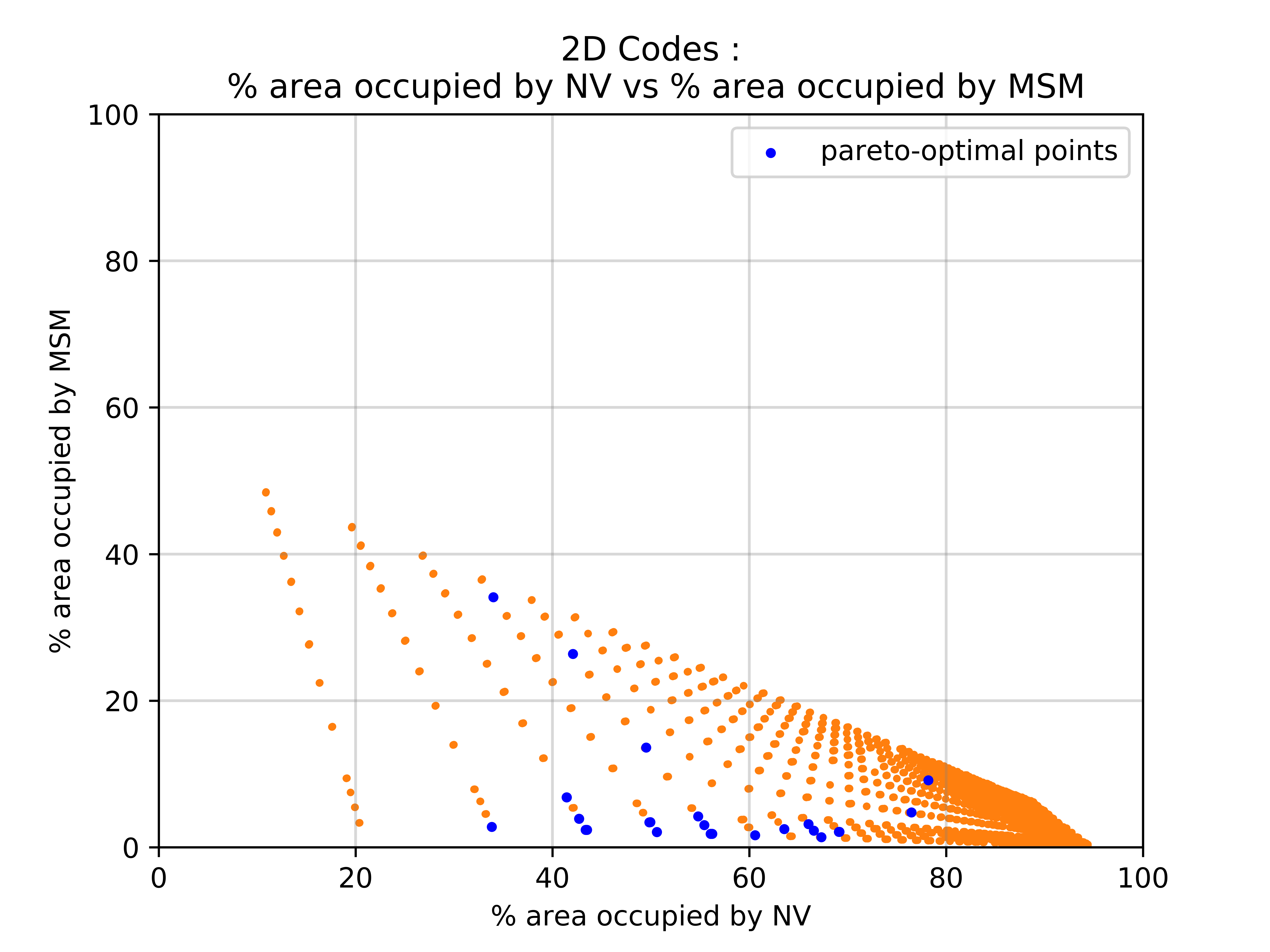
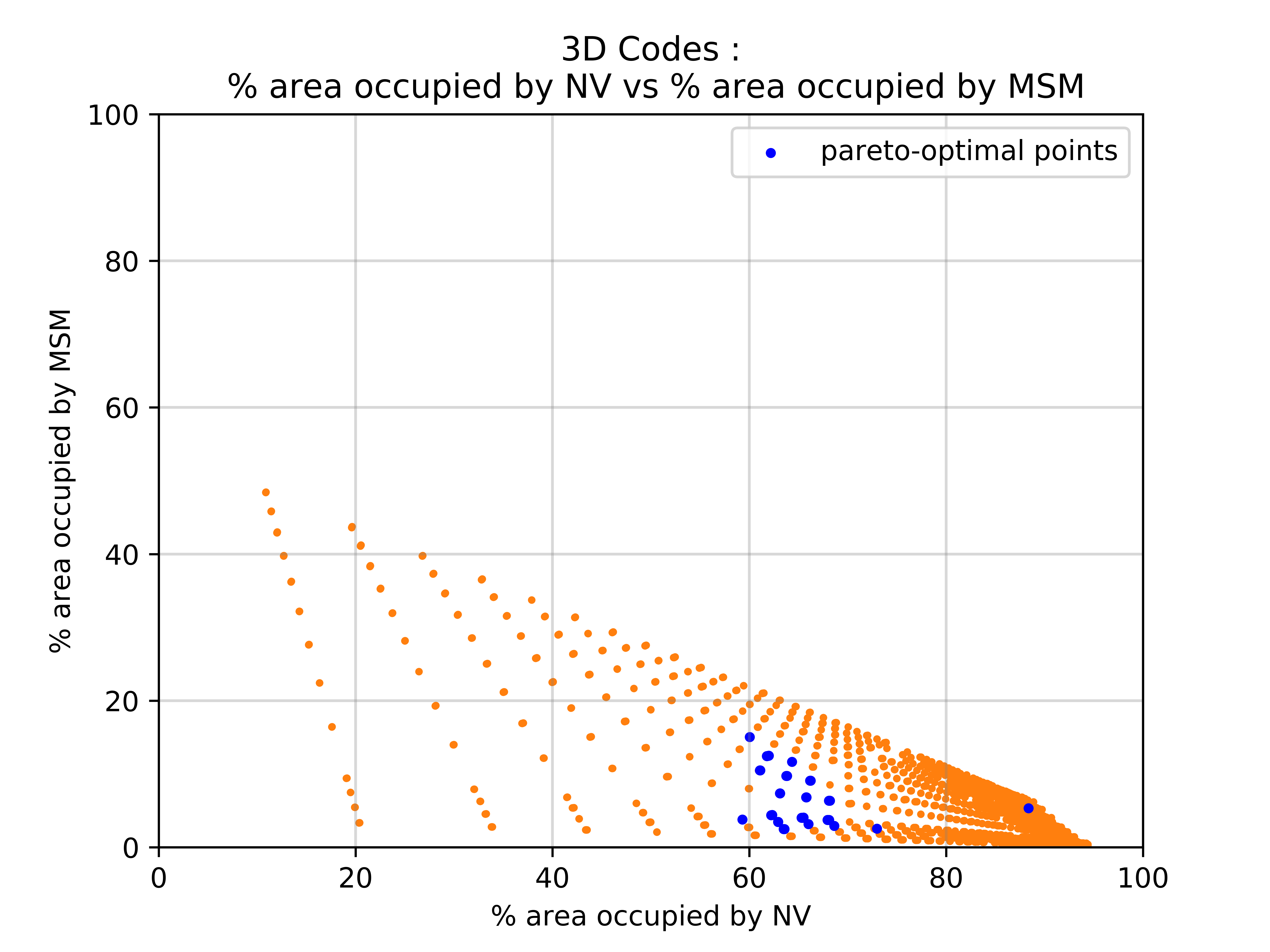
Another interesting perspective is seen in Figure 4 which plots the same design space as in Figure 3 but this time the axes are different, showing the relative percentages of the chip area devoted to memory, and to vector units. We notice the that optimal designs (blue points lie in a relative cluster. This phenomenon is even more marked for 3D stencils. At present, we do not have a clear explanation for why the points are clustered in this manner, an we plan to mine this data to determine patterns in the data.
V-D Discussion
The designer can choose to fix some parameters and optimize for others. Given an application, if the architecture parameters are fixed, the designer can use our approach to optimize for compiler parameters. On the other hand, if only some of the architecture parameters are fixed, if the number of vector units and the size of memories is fixed, then the designer can use our approach to tune for the number of SMs.
One limitation of our current model is register usage. It is known to be critical for performance, e.g., the size of the register file constrains the optimal tile sizes. Currently, the register file size is a fixed constant in the area model and does not appear in the execution time model. Modeling these effects analytically is an ongoing effort.
One must, however, take this with a grain of salt. Our models are approximate and there are other parameters that can play an important role in the design process. For instance, the designer might be interested in optimizing for both execution time as well as power simultaneously. Our approach can be extended to consider energy/power consumption into account. If the energy consumption details of the individual components of the architecture are known, then the objective function can be updated to be the argmin of the weighted execution times and energy components where we seek to maximize the performance. Such an optimization function can be formulated to solve power-gating problems where the designer wants to turn off certain parts of the chip.
Finally, we want to note two important aspects of this work. First, our area model is relatively simplistic, and second, the workload that we have chosen is rather artificial. Nevertheless, we have seen interesting patterns. We expect that designers in the field that have more precise (and probably proprietary) information about their specific context could easily add precision to our model and gather much more sophisticated conclusions.
VI Related work
Our research draws upon prior work in three distinct areas.
VI-A Chip Reverse Engineering and Area Modeling
Chip area modeling can be formally considered a branch of semiconductor reverse engineering, which is a well researched subject area. Torrence et. al. [35] gives an overview of the various techniques used for chip reverse engineering. The packaged chips are usually decapped and the wafer die within is photographed layer by layer. The layers are exposed in the reverse order after physical or chemical exfoliation. Degate [5], for example, is a well known open source software that can help in analyzing die photographs layer by layer. The reverse engineering process can be coarse-grained to identify just the functional macro-blocks. Sometimes, the process can be very fine-grained, in order to identify standard-cell interconnections, and hence, actual logic-gate netlists. Degate is often used in association with catalogs of known standard cell gate layouts, such as those compiled by Silicon Zoo [33]. Courbon et. al. [4] provides a case study of how a modern flash memory chip can be reverse engineered using targeted scanning electron microscope imagery. For chip area modeling, one is only interested in the relatively easier task of demarcating the interesting functional blocks within the die.
VI-B Performance Modeling
There have been various works on time modeling and performance optimization.
Polymage [23] provides a stencil graph DSL and pairs it it with a simple analytical performance model for the automatic computation of optimal tile sizes and fusion choices. With MODESTO [17] an analytical performance model has been proposed that allows to model multiple cache levels and fusion strategies for both GPUs and CPUs as they arise in the context of Stella. For stencil GPU code generation strategies that use redundant computations in combination with ghost zones an analytical performance model has been proposed [21] that allows to automatically derive “optimal” code generation parameters. Yotov et. al [39] showed already more than ten years ago that an analytical performance model for matrix multiplication kernels allows to generate code that is performance-wise competitive to empirically tuned code generated by ATLAS [37], but at this point no stencil computations have been considered. Shirako et al. [32] use cache models to derive lower and upper bounds on cache traffic, which they use to bound the search space of empirical tile-size tuning. Their work does not consider any GPU specific properties, such as shared memory sizes and their impact on the available parallelism. In contrast to tools for tuning, Hong and Kim [18] present a precise GPU performance model which shares many of the GPU parameters we use. It is highly accurate, low level, and requires analyzing the PTX assembly code. For stencil GPU code generation strategies that use redundant computations in combination with ghost zones an analytical performance model has been proposed [21] that allows to automatically derive “optimal” code generation parameters.
VI-C Hardware/Software Codesign
Application codesign is is a well established discipline and has seen active research for well over two decades [28, 38, 2, 6, 34]. The essential idea is to start with a program (or a program representation, say in the form of a CFDG—Control Data Flow Graph) and then map it to an abstract hardware description, often represented as a graph of operators and storage elements. The challenge that makes codesign significantly harder than compilation is that the hardware is not fixed, but is also to be synthesized. Most systems involve a search over a design space of feasible solutions, and various techniques are used to solve this optimization problem: tabu search and simulated annealing [10, 11] integer linear programming [24].
There is some recent work on accurately modeling the design space, especially for regular, or affine control programs [26, 40, 41]. However, all current approaches solve the optimization problem for a single program at a time. To the best of our knowledge, no one has previously considered the generalized application codesign problem, seeking a solution for a suite of programs.
There are multiple publications on codesign related to exascale computing, but they focus on different aspects. For instance, Dosanji et a. [8] focus on methodological aspects of exploring the design space, including architectural testbeds, choice of mini-applications to represent applications codes, and tools. The ExaSAT framework [36] was developed to automatically extract parameterized performance models from source code using compiler analysis techniques. Performance analysis techniques and tools targeting exascale and codesign are discussed in [31].
VII Conclusion
We develop a framework for software-hardware codesign that allows the simultaneous optimization of software and hardware parameters. It assumes having analytical models for performance, for which we use execution time, and cost, for which we choose the chip area. We make use of the execution time model from Prajapati et al [27] that predicts the execution times of a set of stencil programs. For the chip area, we develop an analytical model that estimates the chip area of parameterized designs from the Maxwell GPU architecture. Our model is reasonably accurate for estimating the total die area based on individual components such as the number of SMs, the number of vector units, the size of memories, etc.
We formulate a codesign optimization problem using the time model and our area model for optimizing the compiler and architecture parameters simultaneously. We predict an improvement in the performance of 2D stencils by (104% and 69%) and 3D stencils by (123% and 126%) over existing Maxwell (GTX980 and Titan X) architectures.
The main focus of this paper is not on making specific design recommendations, but rather on the methodology; specifically, to develop a software-hardware codesign framework and to illustrate how models built using it can be used for efficient exploration of the design space for identifying Pareto-optimal configurations and analyzing for design tradeoffs. The same framework, possibly with some modifications, could be used for codesign on other type of hardware platforms (instead of GPU), other type of software kernels (instead of the set of stencils we chose, or even non-stencil kernels), and other kind of performance and cost criteria (e.g., energy as cost). Also, with work focused on the individual elements of the framework, the execution time and the chip area models we used could possibly be replaced by ones with better features in certain aspects or scenarios.
Despite this caveat, the analyses from this paper indicate the following accelerator design recommendations, for the chosen performance, cost criteria, and application profile:
-
•
Remove caches completely and
-
•
Use the area (previously devoted to caches) to add more cores on the chip.
-
•
The more precise the workload characterization and the specific area model parameters, the more useful the conclusions drawn from the study.
References
- [1] Bonmin Project Page. https://projects.coin-or.org/Bonmin, 2015 (accessed March 11, 2016).
- [2] Karam S. Chatha and Ranga Vemuri. MAGELLAN: Multiway hardware-software partitioning and scheduling for latency minimization of hierarchical control-dataflow task graphs. In Proceedings of the Ninth International Symposium on Hardware/Software Codesign, CODES ’01, pages 42–47, New York, NY, USA, 2001. ACM.
- [3] C. Chen, J. Chame, and M. Hall. Chill: A framework for composing high-level loop transformations. Technical Report TR-08-897, USC Computer Science Department, June 2008.
- [4] Franck Courbon, Sergei Skorobogatov, and Christopher Woods. Reverse engineering flash eeprom memories using scanning electron microscopy. In Proceedings of International Conference on Smart Card Research and Advanced Applications, CARDIS 2016: Smart Card Research and Advanced Applications, LNCS Volume 10146, pages 57–72, 2016.
- [5] Degate. http://www.degate.org/documentation/.
- [6] R. P. Dick and N. K. Jha. MOGAC: A multiobjective genetic algorithm for hardware-software cosynthesis of distributed embedded systems. Trans. Comp.-Aided Des. Integ. Cir. Sys., 17(10), November 2006.
- [7] Hristo Djidjev. Codesign mapping and optimization algorithms. Technical Report LA-UR-11-10169, Los Alamos National Laboratory, 2011.
- [8] S. S. Dosanjh, R. F. Barrett, D. W. Doerfler, S. D. Hammond, K. S. Hemmert, M. A. Heroux, P. T. Lin, K. T. Pedretti, A. F. Rodrigues, T. G. Trucano, and J. P. Luitjens. Exascale design space exploration and co-design. Future Gener. Comput. Syst., 30:46–58, January 2014.
- [9] S. Eidenbenz, K. Davis, A. Voter, H. Djidjev, L. Gurvitz, C. Junghans, S. Mniszewski, D. Perez, N. Santhi, and S. Thulasidasan. Optimization principles for codesign applied to molecular dynamics: Design space exploration, performance prediction and optimization strategies. In Proceedings of the U.S. Department of Energy Exascale Research Conference, pages 64–65, 2012.
- [10] Petru Eles, Zebo Peng, Krzysztof Kuchcinski, and Alexa Doboli. System level hardware/software partitioning based on simulated annealing and tabu search. Trans. on Design Automation for Embedded Systems, 2(1):5–32, January 1997.
- [11] C. Erbas, S. Cerav-Erbas, and A. D. Pimentel. Multiobjective optimization and evolutionary algorithms for the application mapping problem in multiprocessor system-on-chip design. IEEE Transactions on Evolutionary Computation, 10(3):358–374, September 2006.
- [12] P. Feautrier. Dataflow analysis of array and scalar references. International Journal of Parallel Programming, 20(1):23–53, Feb 1991.
- [13] Paul Feautrier. Some efficient solutions to the affine scheduling problem. Part I. one-dimensional time. Int. J. of Par. Prog., 21(5):313–347, 1992.
- [14] Paul Feautrier. Some efficient solutions to the affine scheduling problem. Part II. multidimensional time. Int. J. of Par. Prog., 21(6):389–420, 1992.
- [15] Fritzchens Fritz’s collection of nvidia die photographs. https://www.flickr.com/photos/130561288@N04, 2017. Accessed: 2017-April-07.
- [16] Tobias Grosser, Albert Cohen, Justin Holewinski, P. Sadayappan, and Sven Verdoolaege. Hybrid hexagonal/classical tiling for GPUs. In CGO, page 66, Orlando, FL, Feb 2014.
- [17] Tobias Gysi, Tobias Grosser, and Torsten Hoefler. Modesto: Data-centric analytic optimization of complex stencil programs on heterogeneous architectures. In Proc. of the 29th ACM on Int. Conf. on Supercomputing, ICS ’15, pages 177–186, New York, NY, USA, 2015. ACM.
- [18] Sunpyo Hong and Hyesoon Kim. An analytical model for a gpu architecture with memory-level and thread-level parallelism awareness. In Proc. of the 36th Annual Int. Symposium on Computer Architecture, ISCA ’09, pages 152–163, New York, NY, USA, 2009. ACM.
- [19] HP Labs Cacti 6.5 sram area and power estimation tool. https://github.com/HewlettPackard/cacti, 2014. Accessed: 2017-May-31.
- [20] Robin Lee, Jung-Ping Yang, Chia-En Huang, Chih-Chieh Chiu, Wei-Shuo Kao, Hong-Chen Cheng, Hong-Jen Liao, and Jonathan Chang. A 28nm high-k metal-gate sram with asynchronous cross-couple read assist (ac2ra) circuitry achieving 3x reduction on speed variation for single ended arrays. In Proc., IEEE VLSIC 2012, pages 64–65, 2012.
- [21] Jiayuan Meng and Kevin Skadron. Performance modeling and automatic ghost zone optimization for iterative stencil loops on gpus. In Proceedings of the 23rd International Conference on Supercomputing, ICS ’09, pages 256–265, New York, NY, USA, 2009. ACM.
- [22] Susan M. Mniszewski, Christoph Junghans, Arthur F. Voter, Danny Perez, and Stephan J. Eidenbenz. Tadsim: Discrete event-based performance prediction for temperature-accelerated dynamics. ACM Trans. Model. Comput. Simul., 25(3):15:1–15:26, April 2015.
- [23] Ravi Teja Mullapudi, Vinay Vasista, and Uday Bondhugula. Polymage: Automatic optimization for image processing pipelines. In Proceedings of the Twentieth International Conference on Architectural Support for Programming Languages and Operating Systems, ASPLOS ’15, pages 429–443, New York, NY, USA, 2015. ACM.
- [24] Ralf Niemann and Peter Marwedel. An algorithm for hardware/software partitioning using mixed integer linear programming. Design Automation for Embedded Systems, 2(2):165–193, 1997.
- [25] NVidia GeForce GTX-980 photomicrograph. http://international.download.nvidia.com/geforce-com/international/images/geforce-gtx-980-970-feature-article/Maxwell_Die_FlatShade_colorA.jpg, 2014. Accessed: 2016-April-08.
- [26] Louis-Noel Pouchet, Peng Zhang, P. Sadayappan, and Jason Cong. Polyhedral-based data reuse optimization for configurable computing. In Proc. of the ACM/SIGDA Int. Symp. on Field Programmable Gate Arrays, FPGA ’13, pages 29–38, New York, NY, USA, 2013. ACM.
- [27] Nirmal Prajapati, Waruna Ranasinghe, Sanjay Rajopadhye, Rumen Andonov, Hristo Djidjev, and Tobias Grosser. Simple, accurate, analytical time modeling and optimal tile size selection for gpgpu stencils. In Proceedings of the 22nd ACM SIGPLAN Symposium on Principles and Practice of Parallel Programming, pages 163–177. ACM, 2017.
- [28] S. Prakash and A. C. Parker. Synthesis of application-specific multiprocessor systems including memory components. In Proc. of the Int. Conf. on Application Specific Array Processors, pages 118–132, Aug 1992.
- [29] P. Quinton and V. Van Dongen. The mapping of linear recurrence equations on regular arrays. J. of VLSI Signal Processing, 1(2), 1989.
- [30] S. V. Rajopadhye, S. Purushothaman, and R. M. Fujimoto. On synthesizing systolic arrays from recurrence equations with linear dependencies. In Proceedings, Sixth Conference on Foundations of Software Technology and Theoretical Computer Science, pages 488–503, New Delhi, India, December 1986. Springer Verlag, LNCS 241.
- [31] Martin Schulz, Jim Belak, Abhinav Bhatele, Peer Timo Bremer, Greg Bronevetsky, Marc Casas, Todd Gamblin, Katherine E. Isaacs, Ignacio Laguna, Joshua Levine, Valerio Pascucci, David Richards, and Barry Rountree. Performance analysis techniques for the exascale co-design process, volume 25 of Advances in Parallel Computing, pages 19–32. Elsevier, 2014.
- [32] Jun Shirako, Kamal Sharma, Naznin Fauzia, Louis-Noël Pouchet, J. Ramanujam, P. Sadayappan, and Vivek Sarkar. Analytical bounds for optimal tile size selection. In Proc. of the 21st Int. Conf. on Compiler Construction, pages 101–121, Berlin, Heidelberg, 2012. Springer.
- [33] Silicon Zoo open source standard cell catalog. http://www.siliconzoo.org, 2017. Accessed: 2017-April-07.
- [34] J. Teich. Hardware/software codesign: The past, the present, and predicting the future. Proc. of the IEEE, 100:1411–1430, May 2012.
- [35] Randy Torrance and Dick James. The State-of-the-Art in IC Reverse Engineering. In Proceedings of Cryptographic Hardware and Embedded Systems Conference (CHES), LNCS Volume 5747, pages 363–381, 2009.
- [36] Didem Unat, Cy Chan, Weiqun Zhang, Samuel Williams, John Bachan, John Bell, and John Shalf. Exasat: An exascale co-design tool for performance modeling. The International Journal of High Performance Computing Applications, 29(2):209–232, 2015.
- [37] R. Clint Whaley, Antoine Petitet, and Jack J. Dongarra. Automated empirical optimizations of software and the ATLAS project. Parallel Computing, 27(1–2):3–35, 2001.
- [38] Wayne Wolf and Jorgen Staunstrup. Hardware/Software CO-Design: Principles and Practice. Kluwer, Norwell, MA, USA, 1997.
- [39] Kamen Yotov, Xiaoming Li, Gang Ren, Michael Cibulskis, Gerald DeJong, Maria Garzaran, David Padua, Keshav Pingali, Paul Stodghill, and Peng Wu. A comparison of empirical and model-driven optimization. In Proc. of the ACM SIGPLAN Conf. on Programming Language Design and Implementation, pages 63–76, New York, NY, USA, 2003. ACM.
- [40] Wei Zuo, Warren Kemmerer, Jong Bin Lim, Louis-Noël Pouchet, Andrey Ayupov, Taemin Kim, Kyungtae Han, and Deming Chen. A polyhedral-based systemc modeling and generation framework for effective low-power design space exploration. In Proceedings of the IEEE/ACM International Conference on Computer-Aided Design, ICCAD ’15, pages 357–364, Piscataway, NJ, USA, 2015. IEEE Press.
- [41] Wei Zuo, Peng Li, Deming Chen, Louis-Noël Pouchet, Shunan Zhong, and Jason Cong. Improving polyhedral code generation for high-level synthesis. In Proc. of the Ninth IEEE/ACM/IFIP Int. Conf. on Hardware/Software Codesign and System Synthesis, CODES+ISSS ’13, pages 15:1–15:10, Piscataway, NJ, USA, 2013. IEEE Press.