Open-Access Full-Duplex Wireless
in the ORBIT Testbed
Abstract
In order to support experimentation with full-duplex (FD) wireless, we recently integrated an open-access FD transceiver in the ORBIT testbed [1]. In this report, we present the design and implementation of the FD transceiver and interfaces, and provide examples and guidelines for experimentation. In particular, an ORBIT node with a National Instruments (NI)/Ettus Research Universal Software Radio Peripheral (USRP) N210 software-defined radio (SDR) was equipped with the Columbia FlexICoN Gen-1 customized RF self-interference (SI) canceller box. The RF canceller box includes an RF SI canceller that is implemented using discrete components on a printed circuit board (PCB) and achieves RF SI cancellation across bandwidth. We provide an FD transceiver baseline program and present two example FD experiments where and overall SI cancellation is achieved for a simple waveform and PSK modulated signals across both the RF and digital domains. We also discuss potential FD wireless experiments that can be conducted based on the implemented open-access FD transceiver and baseline program.
I Introduction
Due to its potential to double network capacity at the physical (PHY) layer and to provide many other benefits at higher layers, full-duplex (FD) wireless has drawn significant attention [2, 3, 4]. The major challenge associated with FD is the extremely strong self-interference (SI) on top of the desired signal, requiring more than of self-interference cancellation (SIC) across both the RF and digital domains.
Our work on FD transceivers/systems within the Columbia FlexICoN project [5] focuses on integrated circuit (IC) implementations that are appropriate for mobile and small-form-factor devices [4, 6, 7]. In [8], we presented the FlexICoN Gen-1 FD transceiver and an FD wireless link, featuring RF SIC across . The implemented Gen-1 RF SI canceller emulates its RFIC counterpart that we presented in [6] and modeled and analyzed in [9].
However, there is no existing open-access wireless testbed with FD-capable nodes, which is crucial for experimental evaluations of FD-related algorithms at the higher layers. Therefore, to facilitate research in this area and to allow the broader community to experiment with FD wireless, we integrated an improved version of the Gen-1 RF canceller presented in [8] with a National Instruments (NI)/Ettus Research USRP N210 SDR in the open-access ORBIT wireless testbed [1]. Since interfacing an RFIC canceller with an SDR presents numerous technical challenges, we implemented the RF canceller on a printed circuit board (PCB) to facilitate the cross-layered experiments with an SDR platform.
In this technical report, we present our cross-layered (hardware and software) implementation of an open-access FD transceiver integrated with the ORBIT testbed, including the design and implementation of the customized Gen-1 RF canceller box and an FD transceiver baseline program. We also present two example FD experiments that run remotely in the ORBIT testbed, where SIC is performed across both the RF and digital domains, demonstrating the FD capability in the ORBIT testbed. The first example is based on UHD [10], where overall SIC is achieved for a simple waveform. The second example is based on GNU Radio [11], where overall SIC is achieved for PSK modulated signals. The code for the baseline program and a tutorial for the FD transceiver are available at [12, 13]. The implemented FD transceiver and the baseline program, which can be further extended to more complicated communication networking scenarios, can allow the broader community to experiment with FD wireless.
II The FlexICoN Gen-1 RF Canceller Box
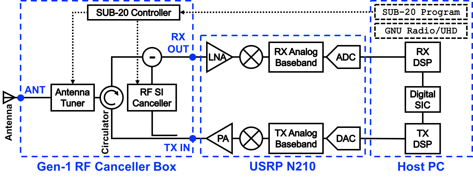
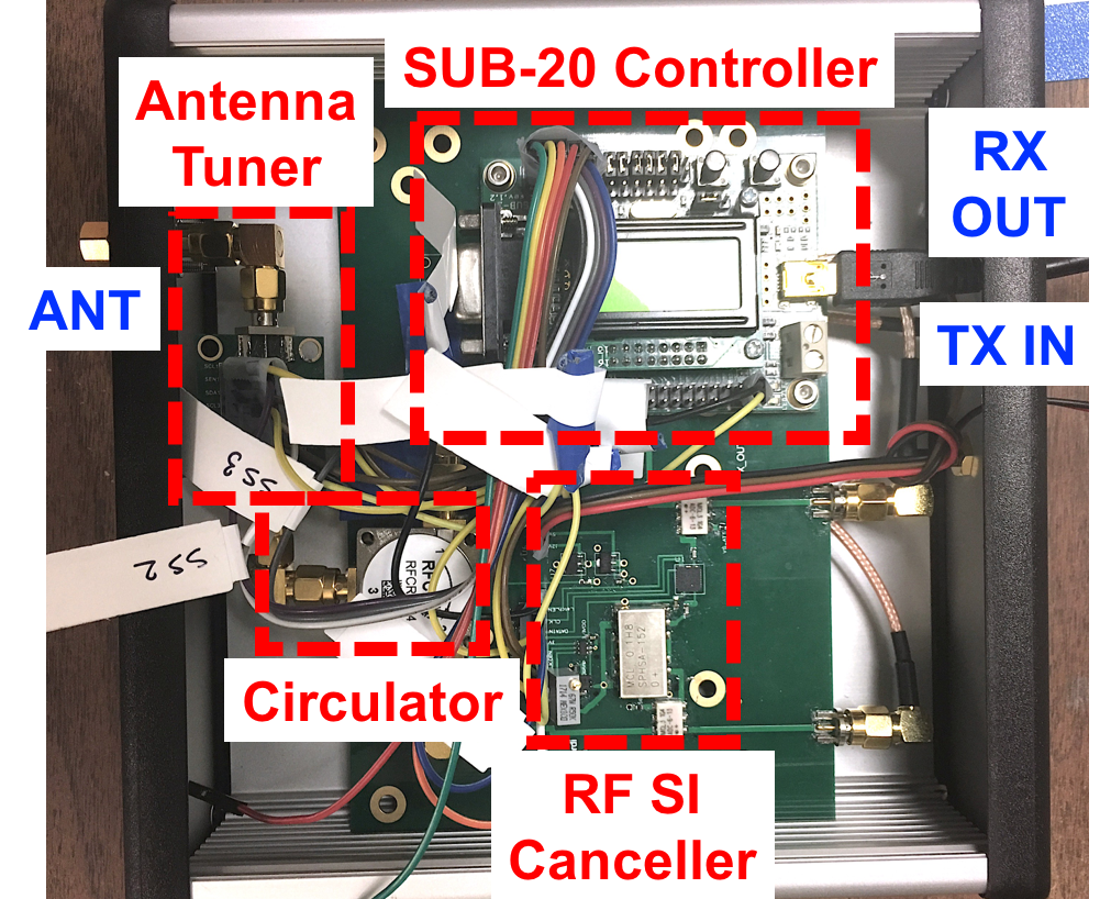
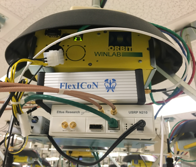
Fig. 1 shows the block diagram of the implemented FD transceiver, in which a Gen-1 RF canceller box (as depicted in Fig. 2LABEL:sub@fig:orbit-node-canc) is connected to an Apex II multi-band antenna (at the ANT port) and a USRP (at the TX IN and RX OUT ports). Fig. 2LABEL:sub@fig:orbit-node-sdr shows the FD transceiver installed in the ORBIT testbed. Specifically, a circulator is used at the antenna interface so that a single antenna can be shared between the TX and RX. To alleviate the RX front-end linearity and the analog-to-digital converter (ADC) dynamic range requirements, sufficient SI isolation and cancellation in the RF domain are needed before digital SIC is engaged.
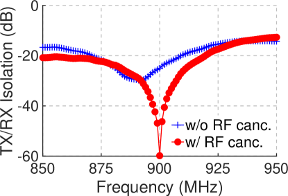
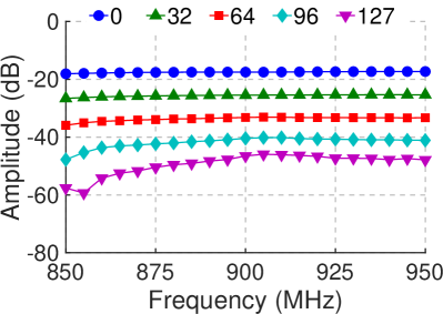
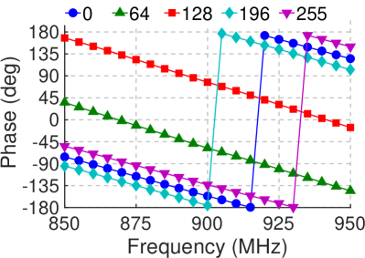
In the FD transceiver, the RF SI suppression is achieved by the circulator and the RF SI canceller in the Gen-1 RF canceller box, where the circulator has a TX/RX isolation of around and the RF SI canceller can provide - RF SIC. As Fig. 2LABEL:sub@fig:orbit-node-canc shows, the RF canceller box contains four components: (i) a frequency-flat amplitude- and phase-based RF canceller, which is an improved version of that presented in [8]111The implemented RF canceller includes a variable gain attenuator with higher resolution and an SPI compared with that presented in [8]., (ii) a coaxial circulator, (iii) a custom-designed antenna tuner, and (iv) a SUB-20 controller. Fig. 3 shows an example of the measured TX/RX isolation (measured between TX IN and RX OUT ports of the canceller box), where RF SIC is achieved across bandwidth.
II-A The Amplitude- and Phase-based RF Canceller
The amplitude- and phase-based RF canceller is implemented using discrete components on a PCB and is optimized around operating frequency.222In this implementation, we select operating frequency but this approach can be easily extended to other frequencies (e.g., ). The RF canceller taps a reference signal from the output of the power amplifier (PA) at the TX side (through a Mini-Circuits ADC-6-13+ directional coupler) and adjusts its amplitude and phase. Then, SIC is performed at the input of the low-noise amplifier (LNA) at the RX side.
For amplitude adjustment, a -bit SKY12343-364LF digital attenuator [14] is used, in which the attenuation can be adjusted within a range with a resolution of . As a result, the RF canceller has an amplitude tuning range between and . For phase adjustment, a Mini-Circuits passive SPHSA-152+ phase-shifter [15] is used, which covers full and is controlled by an -bit TI-DAC081S101 digital-to-analog converter (DAC) [16]. Both the attenuator and phase shifter are programmed through the SUB-20 controller serial-to-parallel interface (SPI) with code values ATT (ATTuation) and PS (Phase Shift), respectively, and the parameter configuration ranges are
The attenuator and DAC have supply voltage and the phase shifter has a reference voltage of .
II-B The Coaxial Circulator
An RF-CI RFCR3204 coaxial circulator is used, whose operating frequency is between -.
II-C The Programmable Antenna Tuner
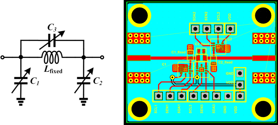
In order for the circulator to better match with varying impedance of the antenna due to environmental changes (around operating frequency), we also designed and implemented a programmable antenna tuner. Fig. 5 shows the circuit diagram and the PCB implementation of the antenna tuner. In particular, a -network with lossless inductor () and digitally tunable capacitors () is used for impedance transformation. In our implementation, we use a fixed chip inductor with inductance and the Peregrine Semiconductor -bit PE64909 digitally tunable capacitors [17] for (). By programming the capacitors with code values CAPi (), different antenna interface impedance matching can be achieved. The corresponding configuration ranges of the tunable capacitors are
II-D The SUB-20 Controller
As Fig. 1 shows, a DIMAX SUB-20 multi-interface USB adapter [18] connected to the host PC is used to program the attenuator and DAC (on the RF SI canceller) and the capacitors (on the antenna tuner) through SPI. The SUB-20 SPI is configured to operate at the maximal master clock of . At this clock rate, programming one ATT or PS value (a -byte word including the address fields, etc.) takes , and programming one CAPi value (a -byte word) takes . We note that other controller platforms with higher SPI clock rates can also be used to improve the performance.
III Integration with the ORBIT Testbed
and an FD Transceiver Baseline Node Image
An ORBIT node equipped with the Gen-1 RF canceller box is depicted in Fig. 2LABEL:sub@fig:orbit-node-sdr. We use node11-10 in the ORBIT main grid with a USRP N210 SDR. In particular, the RF canceller box TX IN/RX OUT ports are connected to the USRP TX/RX ports, respectively, and the RF canceller box ANT port is connected to an Apex II multi-band antenna (see Figs. 1 and 2). We developed an FD transceiver baseline node image, which contains two example FD experiments running on the host PC (i.e., the yellow box in Fig. 2LABEL:sub@fig:orbit-node-sdr): (i) a UHD-based example with a simple waveform, and (ii) a GNU Radio-based example with modulated signals using Phase-Shift Keying (PSK) modulation scheme. Throughout the experiments, the USRP has a receiver noise floor of .333This USRP receiver noise floor is limited by the existence of environmental interference at frequency. The USRP has a true noise floor of around at the same receiver gain setting, when not connected to an antenna.
To facilitate the experiments with the RF canceller box and FD wireless, the customized FD transceiver baseline node image named flexicon-orbit-v2.ndz with the required software was created and stored in the ORBIT testbed. The code for the FD transceiver baseline program is available at https://github.com/Wimnet/flexicon_orbit. The detailed tutorial and instructions containing the steps for running the example FD experiments can be found at [13, 12].
IV An Example FD Experiment based on UHD
In this section, we present an example FD experiment using the FD transceiver and the baseline program, where the FD transceiver transmits and receives simultaneously at carrier frequency with sampling rate. Different from regular UHD programs that are designed for half-duplex applications, the FD UHD program includes three parallel threads for performance optimization: the TX/RX streaming threads running on the same frequency channel and a third thread for executing the digital SIC algorithm. In particular, the digital SIC algorithm is based on Volterra series and a least-square problem and is similar to that presented in [3, 7]. Moreover, the Eigen C++ library is included for computations in the digital SIC algorithm (e.g., matrix operations and FFT).
In this example FD experiment, the FD transceiver (node11-10) sends a single tone with frequency offset at TX power level. Fig. 6 shows an example output of the FD transceiver SUB-20 program, where the RF canceller box is configured with parameters
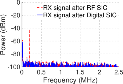
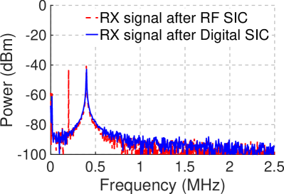
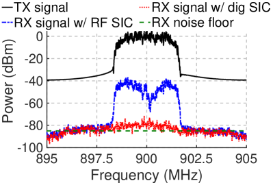
through the C program rf_canc_gen1_config.444The optimal configuration of the RF canceller box may change due to factors such as antenna being re-tightened or rotated. Please refer to the detailed tutorial [13] for updates. Fig. 3 shows the TX/RX isolation of the RF canceller box under this configuration. Fig. 7 shows an example output of the FD transceiver UHD program where overall SIC is achieved, where is from the RF domain and is from the digital SIC algorithm, and the SI signal is canceled to the receiver noise floor. Fig. 8 shows the power spectrum of the residual SI after RF and digital SIC through an offline MATLAB script.
In addition, another ORBIT node (node13-8) serves as a second radio that sends a single tone with frequency offset using the UHD tx_waveforms program [10], i.e.,
Fig. 8 presents the power spectrum of the signal received at the FD transceiver after RF and digital SIC. As Fig. 8 shows, the SI at the FD transceiver (with frequency offset ) is canceled to the receiver noise floor after SIC in both the RF and digital domains, and the digital SIC algorithm introduces minimal SNR loss to the desired signal (with frequency offset ).
V An Example FD Experiment based on GNU Radio
In this section, we present another example FD experiment based on GNU Radio, where the FD transceiver transmits a wideband PSK-modulated signals. Compared with the UHD-based example, GNU Radio provides both user-friendly implementation and a graphical user interface (GUI) but it also has performance limitations, as will be explained below.
To integrate the RF canceller configuration with the main GNU Radio program, we implemented a customized GNU Radio out-of-tree (OOT) SUB-20 module. Given the relatively stable wireless environment in the ORBIT testbed, the OOT SUB-20 module is implemented with fixed555Users can change CAPi using the SUB-20 C program (see Section IV). , , and users can vary the values of ATT and PS to observe different RF SIC performance. This example FD experiment contains three parts:
-
1.
Data Generation: The baseband samples encoding raw bits modulated using an PSK scheme (e.g., BPSK and QPSK) are generated using gen_data_psk;
-
2.
Data Transmission and RF SIC: The FD transceiver transmits the modulated samples and receives samples over-the-air using usrp_txrx_psk. The RF canceller can be configured in real-time to observe different RF SIC performance;
-
3.
Digital SIC: The digital SIC is performed offline using dig_sic_on and the received baseband samples.
Due to the software and timing limitations of GNU Radio, baseband samples are recorded using the file option and digital SIC is performed offline (part 3). We remark that other implementations (e.g., UHD- or FPGA-based) may be able to support digital SIC in real-time.
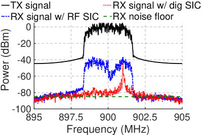
A GNU Radio-based example experiment was demonstrated in [19] where the FD transceiver (node11-10) transmits a QPSK signal stream with QPSK modulation scheme at sampling rate and average TX power level. Fig. 9LABEL:sub@fig:exp-psk-node shows the power spectrum of the received signal at the FD transceiver, where overall SIC is achieved, where is from the RF domain and is from the digital domain. The SI signal is canceled to the USRP receiver noise floor at TX power. Another ORBIT node (node13-8) is then used to serve as a second radio that transmits a single tone with a frequency offset of . As Fig. 9LABEL:sub@fig:exp-psk-link shows, the desired signal is recoved after the SIC (in both the RF and digital domains) is performed at the FD transceiver.
VI Other Potential FD Wireless Experiments
Some potential FD experiments that can be conducted using the presented FD transceiver are listed below:
-
-
Hands-on experiments with FD wireless on an SDR platform in a teaching/lab course;
-
-
Studying different RF SIC performance and its relation to the antenna interface response by tuning the RF canceller box (the SUB-20 C program or the OOT SUB-20 module);
-
-
Studying the performance of the digital SIC algorithm by tuning its parameters (digital SIC part of the GNU Radio/UHD program);
-
-
Development and evaluation of different digital SIC algorithms (digital SIC part of the GNU Radio/UHD program);
-
-
Incorporation of modulated signals, such as OFDM, with different bandwidth (the GNU Radio/UHD program);
-
-
Experimentation and evaluation of medium access control (MAC) algorithms in a heterogeneous network with an FD access point/client (e.g., modifying the GNU Radio/UHD program and adding a MAC layer).
VII Conclusion
In this report, we presented our cross-layered (hardware and software) design and implementation of the first open-access remotely-accessible FD transceiver which is integrated with the ORBIT wireless testbed. An FD transceiver baseline program and an example FD experiment were provided to facilitate the experimentation with the FD transceiver. We discussed other potential FD experiments that can be developed and conducted using the FD transceiver.
Our future work includes the integration of the Gen-2 canceller box in both the ORBIT testbed and the PAWR COSMOS testbed. In particular, we demonstrated the Gen-2 RF canceller in [20], which can achieve wideband RF SIC via the technique of frequency-domain equalization. The Gen-2 RF SI canceller implemented on a PCB emulates its RFIC counterpart we presented in [21]. We plan to install more FD transceivers in the ORBIT and COSMOS testbeds with both Gen-1 and Gen-2 RF canceller boxes. Our future work also includes developing more advanced FD-related software and applications.
Acknowledgments
This work was supported in part by NSF grants ECCS-1547406 and CNS-1827923, DARPA RF-FPGA program, DARPA SPAR program, a Qualcomm Innovation Fellowship, Texas Instruments, Intel, and a National Instruments Academic Research Grant. We thank Steven Alfano, Jelena Diakonikolas, Aishwarya Rajen, Jinhui Song, Mingyan Yu for their contributions to various aspects of the project. We thank Ivan Seskar, Jakub Kolodziejski, and Prasanthi Maddala from WINLAB, Rutgers University, for their help on the integration with the ORBIT testbed. We also thank Kira Theuer and Kendall Ruiz from NI and the NI technical support team for their help.
References
- [1] “Open-access research testbed for next-generation wireless networks (ORBIT),” http://www.orbit-lab.org/.
- [2] A. Sabharwal, P. Schniter, D. Guo, D. W. Bliss, S. Rangarajan, and R. Wichman, “In-band full-duplex wireless: Challenges and opportunities,” IEEE J. Sel. Areas Commun., vol. 32, no. 9, pp. 1637–1652, 2014.
- [3] D. Bharadia, E. McMilin, and S. Katti, “Full duplex radios,” in Proc. ACM SIGCOMM’13, 2013.
- [4] J. Zhou, N. Reiskarimian, J. Diakonikolas, T. Dinc, T. Chen, G. Zussman, and H. Krishnaswamy, “Integrated full duplex radios,” IEEE Commun. Mag., vol. 55, no. 4, pp. 142–151, 2017.
- [5] “The Columbia FlexICoN project,” http://flexicon.ee.columbia.edu/.
- [6] J. Zhou, A. Chakrabarti, P. Kinget, and H. Krishnaswamy, “Low-noise active cancellation of transmitter leakage and transmitter noise in broadband wireless receivers for FDD/co-existence,” IEEE J. Solid-State Circuits, vol. 49, no. 12, pp. 1–17, 2014.
- [7] H. Krishnaswamy, G. Zussman, J. Zhou, J. Marašević, T. Dinc, N. Reiskarimian, and T. Chen, “Full-duplex in a hand-held device —- from fundamental physics to complex integrated circuits, systems and networks: An overview of the Columbia FlexICoN project,” in Asilomar’16, 2016.
- [8] T. Chen, J. Zhou, N. Grimwood, R. Fogel, J. Marašević, H. Krishnaswamy, and G. Zussman, “Demo: Full-duplex wireless based on a small-form-factor analog self-interference canceller,” in Proc. ACM MobiHoc’16, 2016.
- [9] J. Marasevic, J. Zhou, H. Krishnaswamy, Y. Zhong, and G. Zussman, “Resource allocation and rate gains in practical full-duplex systems,” IEEE/ACM Trans. Netw., vol. 25, no. 1, pp. 292–305, 2017.
- [10] “USRP Hardware Driver (UHD) software,” https://github.com/EttusResearch/uhd.
- [11] “GNU Radio software,” https://www.gnuradio.org/.
- [12] “The Columbia FlexICoN project: Instructions and code,” https://github.com/Wimnet/flexicon_orbit.
- [13] “Tutorial: Full-duplex wireless in the orbit testbed,” http://www.orbit-lab.org/wiki/Tutorials/k0SDR/Tutorial25, 2017.
- [14] “Skyworks SKY12343-364LF digital attenuator data sheet,” http://www.skyworksinc.com/uploads/documents/201355C.pdf.
- [15] “Mini-Circuits SPHSA-152+ phase shifter data sheet,” https://www.minicircuits.com/pdfs/SPHSA-152+.pdf.
- [16] “Texas Instruments DAC081S101 8-bit digital-to-analog converter data sheet,” http://www.ti.com/lit/ds/symlink/dac081s101.pdf.
- [17] “Peregrine Semiconductor PE64909 digitally tunable capacitor data sheet,” http://www.psemi.com/pdf/datasheets/pe64909ds.pdf.
- [18] “DIMAX SUB-20 user manual,” http://www.xdimax.com/sub20/doc/sub20-man.pdf.
- [19] T. Chen, M. Baraani Dastjerdi, G. Farkash, J. Zhou, H. Krishnaswamy, and G. Zussman, “Demo abstract: Open-access full-duplex wireless in the ORBIT testbed,” in Proc. IEEE INFOCOM’18, 2018.
- [20] T. Chen, J. Zhou, M. Baraani Dastjerdi, J. Diakonikolas, H. Krishnaswamy, and G. Zussman, “Demo abstract: Full-duplex with a compact frequency domain equalization-based RF canceller,” in Proc. IEEE INFOCOM’17, 2017.
- [21] J. Zhou, T.-H. Chuang, T. Dinc, and H. Krishnaswamy, “Integrated wideband self-interference cancellation in the RF domain for FDD and full-duplex wireless,” IEEE J. Solid-State Circuits, vol. 50, no. 12, pp. 3015–3031, 2015.