Tuning Topological Phase Transitions in Hexagonal Photonic Lattices Made of Triangular Rods
Abstract
In this paper, we study topological phases in a 2D photonic crystal with broken time () and parity () symmetries by performing calculations of band structures, Berry curvatures, Chern numbers, edge states and also numerical simulations of light propagation in the edge modes. Specifically, we consider a hexagonal lattice consisting of triangular gyromagnetic rods. Here the gyromagnetic material breaks symmetry while the triangular rods breaks symmetry. Interestingly, we find that the crystal could host quantum anomalous Hall (QAH) phases with different gap Chern numbers () including as well as quantum valley Hall (QVH) phases with contrasting valley Chern numbers (), depending on the orientation of the triangular rods. Furthermore, phase transitions among these topological phases, such as from QAH to QVH and vice versa, can be engineered by a simple rotation of the rods. Our band theoretical analyses reveal that the Dirac nodes at the and valleys in the momentum space are produced and protected by the mirror symmetry () instead of the symmetry, and they become gapped when either or symmetry is broken, resulting in a QAH or QVH phase, respectively. Moreover, a high Chern number () QAH phase is generated by gapping triply degenerate nodal points rather than pairs of Dirac points by breaking symmetry. Our proposed photonic crystal thus provides a platform for investigating intriguing topological phenomena which may be challenging to realize in electronic systems, and also has promising potentials for device applications in photonics such as reflection-free one-way waveguides and topological photonic circuits.
I Introduction
In recent years, electronic and photonic topological insulatorskane10 ; joan14 have attracted enormous attention because these systems exhibit fascinating wave transport properties. In particular, the gapless edge states on the surface or at the interface between these topological insulators are unidirectional and robust against scattering from disorder due to topologically nontrivial properties of their bulk band structures. The electronic quantum anomalous Hall (QAH) phase, first proposed by Haldanehald88 , is a two-dimensional (2D) bulk ferrromagnetic insulator (Chern insulator) with a nonzero topological invariant called Chern number in the presence of spin-orbit coupling (SOC) but in the absence of applied magnetic fields.Weng15 Its associated chiral edge states carry dissipationless unidirectional electric current. Excitingly, this remarkable QAH phase was recently observed in ferromagnetic topological insulator filmsChang13 . Moreover, Haldane and Raghu recently proposed the optical analogs of this intriguing QAH phase in photonic crystals made of time-reversal () symmetry broken materialshald08a ; hald08b . This photonic QAH phase has gapless edge states within each topologically nontrivial bulk band gap, and the number of the edge states is determined by the gap Chern numberhald08b . Such topologically protected edge states are immune to backscattering and are therefore robust against disorder.joan08 ; joan09 Subsequently, the photonic topological phases in a number of gyromagnetic photonic crystals with broken symmetry were proposed joan08 ; he10 ; wang13 ; skir14 and observedjoan09 ; skir15 .
When designing a photonic Chern insulator, one usually starts with a lattice with both symmetry and inversion () symmetry where doubly degenerate Dirac points may exist at some high symmetry points.hald08b In particular, in a 2D lattice with both and symmetries, the stability of the Dirac points is guaranteed by the Wigner-von Neumann theorem. Furthermore, one can find the double degeneracies by varying just one or two system parameters. When symmetry is broken, the Dirac points become gapped, resulting in a QAH phase. Nevertheless, the topological phases in broken symmetry Chern insulators have received much less attention, where different mechanisms would be needed.he15 ; Ono09
Furthermore, majority of the predicted or realized photonic Chern insulators so far have been limited to the Chern number ,joan08 although in principle the Chern number can be any integer values. Consequently, having systems with is of fundamental interest in studying topological phases. Systems with higher Chern numbers also have practical values. For example, they are useful for designing novel topological devices such as one-way photonic circuits.he10 ; wang13 Indeed, it has been recently proposedskir14 and demonstrated skir15 that photonic Chern insulators of large Chern numbers can be realized in 2D square and hexagonal lattices made of cylindrical rods by tuning the radius of the rods. It would be interesting to find other ways to realize photonic Chern insulators with .
Interestingly, recent progress in understanding the novel properties of electronic 2D materials such as graphene and MoS2 monolayer has led to the discovery of a invariant topological phase called qunatum valley Hall (QVH) state in broken symmetry materialsXiao07 ; Niu10 ; Mak14 . In these QVH materials, the energy extrema (or valleys) of the band structure at the and points in their hexagonal Brillouin zone have contrasting properties such as nonzero Berry curvatures of opposite signs due to the absence of symmetry but presence of invariance, although they are energetically degenerate.Xiao07 ; Niu10 ; Mak14 ; Ma16 ; Chen17 This broken valley symmetry results in a number of interesting valley-contrasting phenomena and also a totally new concept of electronics known as valleytronicsXiao07 . Recently, this QVH effect has also been realized in all-dielectric photonic crystalsMa16 ; Chen17 and bianisotropic metamaterialsdong16 , and the valley-protected reflection-free propagation of light in the edge modes of these materials has been demonstrated. This would lead to the fascinating prospect of optical communication devices based on the robust flow of light.
In this paper, we explore possible topological phases in a 2D photonic crystal with broken and symmetries. We consider a hexagonal lattice made of triangular gyromagnetic rods, as illustrated in Fig. 1(a). Here the gyromagnetic material breaks symmetry while the triangular rods breaks symmetry. Interestingly, we find that the crystal hosts QAH phases with different gap Chern numbers including and QVH phases with contrasting valley Chern numbers, depending on the orientation [i.e., the rotation angle in Fig. 1(b)] of the triangular rods. Furthermore, phase transitions among these topological phases, such as from QAH to QVH and vice versa, can be engineered by a simple rotation of angle . Our band theoretical analyses reveal that the Dirac points at the and valleys are produced and protected by the mirror symmetry () instead of the symmetry, and they become topologically gapped when either or symmetry is broken, resulting in a QAH or QVH phase, respectively. Moreover, the high Chern number () QAH phase results from gapping triply degenerate nodal points rather than pairs of Dirac pointsskir14 by breaking symmetry. Thus, our proposed photonic crystal offers a platform for investigating a number of topological phenomena which may be challenging to realize in electronic systems, and also has promising device applications in photonics.
The rest of this paper is organized as follows. First, we introduce the proposed structure and also describe the computational methods in the next section. Then the main results are presented in Sec. III, including the rich topological gap map on the frequency-rod angle plane in Subsec.III.1, the representative bulk band structures in Subsec.III.2, the calculated Berry curvatures in Subsec. III.3, the gapless edge states in Subsec.III.4 and reflection immunne one-way waveguides in III.5 as well as valley Hall edge states and light propagation in Z-shape bends in III.6. Finally, the conclusions drawn from this work are given in Sec. IV.
II Structure and Computational method
Here we consider a 2D photonic crystal consisting of triangular gyromagnetic rods arranged in a hexagonal lattice filled with air, as shown in Fig. 1(a). The symmetry is broken by the gyromagnetic rods used. The permeability tensor of the gyromagnetic material in SI units can be expressed as
| (1) |
Following Ref. [joan08, ], we neglect the small loss and dispersion, and thus set the material parameters , and . Note that these parameter values are close to such real gyromagnetic materials as yttrium-iron-garnet,skir15 ; joan09 which has and at GHz with T static magnetic field.MWbook
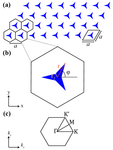
The triangular rods are determined by two geometric parameters and , as indicated in Fig. 1(b). In our numerical simulations, we set and where is the lattice constant. Nevertheless, our conclusions will not be affacted by this perticaular choice of the parameters. The structure will be completely fixed only when the angle () between one of the arms and the -axis is specified [see Fig. 1(b)], and this angle is the principal parameter that one tunes to manipulate the properties of the structure, as will be presented in the next section. The structure has the symmetry with 3 threefold rotations and 3 mirror () reflections, for and . The mirror symmetries contain (reflection plane normal to ) if but include (reflection plane normal to ) if . The Brillouin zone (BZ) is also hexagonal, as shown in Fig. 1(c). However, the irreducbile BZ wedge (IBZW) depends on angle . For example, when , the IBZW is KM since K and K′ are equivalent. In contrast, when , the IBZW is KMK because K and K′ are no longer equivalent [see Fig. 1(c)].
To calculate the band structure of the proposed structure, we solve the Maxwell′s wave equation
| (2) |
where and are the permeability and permittivity tensors, respectively, and is the eigenfrequency. We use the finite-element method implemented in the commercial software COMSOL Multiphysics ®.comsol To examine the topological nature of a band gap in the band structure, we also calculate the band Chern number
| (3) |
where the integral is over the BZ and is the Berry curvature of the th band defined as Niu10
| (4) |
where is the Berry connection and is the th band energy. Here we adopt the efficient numerical algorithm reported in Ref. [Hats05, ] to calculate the band Chern numbers. Note that the Berry curvature and the Chern number are invariant under gauge transformation, while is gauge-dependent. Consequently, one advantage of the algorithm is that we can obtain via Eq. (3) without any gauge-fixing process. Thanks to the efficiency of the algorithm,Hats05 we can obtain the accurate even using a moderate dense -point mesh, and this enables us to perform massive calculations for searching candidate structures or plotting topological gap map such as Fig. 2.skir15
The integer Chern number is the topological invariant of the th energy band. The sum of the Chern numbers of all the bands below a band gap is called the gap Chern number .Hats93 ; skir14 According to the bulk-edge correspondence,Hats93 the number of gapless edge states between two topologically distinct materials equals to the gap Chern number difference across the interface.
III Results and discussion
III.1 Topological gap map
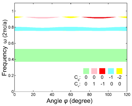
To have an overall picture of the topological phases and phase transitions in the proposed triangular photonic crystal, we construct a topological gap map in the plane of rotation angle and frequency , as displayed in Fig. 2. Since we find that the period of the rotation angle is , we calculate the band gaps as a function of the rotation angle from to with the angle step .
| structure | ||||||
|---|---|---|---|---|---|---|
| gap number | ||||||
| () | 0.16 | 0.056 | 0.021 | 0.16 | 0.041 | 0.018 |
| () | 36 | 7.3 | 2.3 | 35 | 5.2 | 2.0 |
| 0 | -1 | -2 | 0 | -1 | 0 | |
| 0 | 0 | 0 | 0 | 0 | 1 | |
| 0 | 1 | 2 | 0 | 1 | 0 | |
| () | - | 1400 | 6 | - | 23 | - |
Figure 2 shows that there are three band gap regions in the frequency range from 0 to 1 . The topological nature of a band gap in a broken symmetry system can be characterized by the gap Chern number (), which is the sum of the Chern numbers of all the bands below the band gap, as mentioned above in Sec. II. Therefore, the first band gap near 0.5 is topologically trivial because its gap Chern number . The second band gap just below 0.8 is topologically nontrivial and its gap Chern number . Moreover, the band gap is rather large, being around 7 % (0.056 ). Interestingly, when rotationa angle varies from 0 to 120∘, the third band gap experiences a series of topology changes (see Fig. 2). For example, as increases, the topological phase changes from () to () at , and from () to () at . Here is the valley Chern numberNiu10 of the gap (see Subsec. III.4 below). The gap and valley Chern numbers in the vicinity of are and , while they are and () in the region centered at (). Figure 2 thus shows that the angle period is 120∘ rather than 60∘. Although the system has the same Chern number of 0 for and , its valley Chern numbers at these values have opposite signs. Clearly, such a topological gap map provides us useful information for, e.g., designing photonic topological insulators and hence reflection-free one-way waveguides as well as for engineering topological phase transitions. Characteristics of the band gaps for the and cases are listed in Table I.
III.2 Bulk band structures
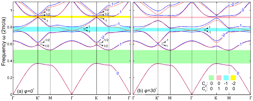
To understand the formation mechanisms of the topological gaps and also other interesting properties of the triangular photonic crystal, we present the calculated band structures for the and cases in Fig. 3(a) and Fig. 3(b), respectively. The TM mode (i.e., ) is considered here. To see how the band structure evolves when dielectric triangular rods are replaced by gyromagnetic rods, both band structures of and are presented. Adding a non-zero off-diagonal element () to the permeability tensor [Eq. (1)] breaks symmetry.
Several observations can be drawn from an examination of Fig. 3. Firstly, when and hence the system has the symmetry, the energy bands (red dotted lines) along the KM and K′M lines are identical [see Fig. 3(a) and Fig. 3(b)]. This is because the symmetry ensures .joanBook Secondly, when and , there are doubly degenerate points (i.e., the Dirac points) at the and points [see red dotted lines near in Fig. 3(a)]. In contrast, the case has no such degenerate points [see red dotted lines in Fig. 3(b)]. This results from the fact that the geometry has 3 mirror reflections (i.e., 3 vertical reflection planes along direction) while the structure lacks such mirror symmetry. In other words, the Dirac points at and points in the structure occur because of the presence of both and symmetries. Thirdly, Figure 3 shows that when , there are doubly degenerate points (i.e., massive Dirac nodes) (see red dotted lines close to ) at the center of the BZ (the point). When the becomes nonzero and hence symmetry is broken, the double degeneracies are lifted and the Dirac nodes become gapped. When these Dirac nodes become gapped due to broken symmetry, the two bands would exchange Berry phase (see Fig. 4), giving rise to a nontrivial gap. Finally, Fig 3 (a) shows that there are triply degenerate nodal points at the and points near . These rare triply degenerate nodal points are caused by the accidental degeneracy of a doubly degenerate Dirac point and a nondegenerate band. Fascinatingly, it was shown that photonic crystals with a triply degenerate nodal point at the point may be used to realize zero-refractive-index metamaterials.Huang11 These interesting three-fold nodal points were recently found in topological phonic crystals.Lu15 More recently, they were also predicted in several electronic topological metalsWeng16 ; Zhu16 and subsequentlty observed in topological semimetal MoPLv17 . All these indicate that the triply degenerate nodal points are attracting increasing attention in the field of electronic, phononic and photonic topological materials.
The topological nature of a band gap in a broken symmetry structure can be characterized by the gap Chern number (), as mentioned before in Sec. II. The calculated band Chern numbers displayed in Fig. 3 indicate that the first band gap with is topologically trivial in both and cases. In contrast, the second band gap is a QAH phase with [see Fig. 3(a) and Fig. 3(b)]. Note that this band gap results from the lifting of the doubly degenerate Dirac nodes at the point by breaking the symmetry, which exist in both and cases. Remarkably, in the case the third band gap is a high Chern number QAH phase with [Fig. 3(a)]. This interesting band gap results from gapping the rare triply degenerate nodal points at the and points by broken symmetry (). Thus, the gap Chern number () is larger than 1. Interestingly, this large Chern number gap would allow us to create multi-mode one-way edge states and hence waveguides.skir14 In the case, on the other hand, the band gap is a QVH phase with valley Chern number [Fig. 3(b)], which will be discussed in the next Subsec. Note that the third gap already occurs when and thus is not caused by broken symmetry [Fig. 3(b)]. Instead, it results from broken mirror symmetry. Nonetheless, when becomes nonzero (e.g., ), this gap at the point becomes larger. Interestingly, in contrast, this gap at the point becomes smaller when becomes nonzero.
Lastly, Fig. 3 shows that when becomes nonzero, there is no direct overlap between bands 2 and 3 in the entire BZ. Note that there is a small gap between bands 2 and 3 at in Fig. 3(b). In other words, there is a continuous gap separating bands 2 and 3 throughout the BZ and hence bands 2 and 3 have a well-defined band Chern number. Furthermore, this gap is topologically nontrivial since it has a nonzero gap Chern number of . Nonetheless, this gap is not marked on the gap map in Fig. 2 simply because it is not a complete gap due to the indirect overlap between bands 2 and 3.
III.3 Berry curvatures
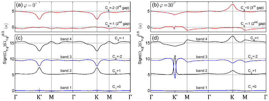
In order to unravel how the numbers exchange between neighboring bands as well as the resultant arises, we calculate the band Berry curvatures for all the four bands below the third band gap (see Fig. 3) and plot these Berry curvatures for and in Fig. 4. Note that in Fig. 4 we plot sign( in order to better reveal the variation of the Berry curvatue with . Here we follow Ref. [Guo08, ] where the band-decomposed spin Berry curvatures helped to reveal the origin of the gigantic spin Hall conductivity in platinum metal. It turns out that gapping the degenerate points at and cause quite different Berry curvatures. We also evaluate the gap Berry curvatures given by
| (5) |
where the summation is over all the band Berry curvature below the gap. An integration of over the BZ gives rise to the gap Chern number .skir14 The calculated for the second and third gaps for and are displayed as a function of in Fig. 4. The contour plots of on the plane for the third gap for and are given in Fig. 5.
Figure 4(a) shows that for bands 2-4, all the band Berry curvatures peak at and . Furthermore, the signs of the peaks for bands 2 and 3 are opposite. As mentioned before, with the symmetry, the nd and rd bands touch at and and thus form the massless Dirac points [Fig. 3(a)]. However, when the symmetry is broken, these Dirac points become gapped and the nd and rd bands exchange Berry phase [Berry phase given by Eq. (3)] and hence . This gives rise to the peaks with opposite signs in at these Dirac points. Interestingly, if both bands are below the gap of interest, their contributions to the gap Chern number cancel each other and thus become diminished. Therefore, in the present case, the main contribution to the gap Berry curvature and hence the gap Chern number of the third gap comes mainly from the 4th band which has the pronounced peaks at and [Fig. 4(a)]. Interestingly, in the case of , bands 2 and 3 have a large peak at but a small peak at . Nevertheless, these two peaks with opposite signs cancel each other and hence the dominant contribution to the gap Berry curvature comes predominantly from band 4. However, the band Berry curvatures of band 4 in the regions centered at and have opposite signs [see Fig. 4(b) and Fig. 5(b)] and consequently, the gap Chern number of the third gap is zero. In contrast, Fig. 4 shows that the of the second gap () varies more smoothly over the BZ, and this could be attributed to the much larger gap openned at the massive Dirac point on the point. Finally, this has a small peak at instead (Fig. 4).
Figures 3 and 4 can also help us to better understand how exchange at the degenerate points when the symmetry is broken. For instance, Fig. 4(c) shows that both and have a peak at the and , but with opposite signs. This suggests that band 2 and band 3 exchange Chern number at and , as illustrated by the black arrows at and in Fig. 3(a). Likewise, and have similar behaviors near the . Here the exchanged Chern numbers have opposite signs and this is because gapping the Dirac point at would result in an exchange of Chern numbers. Indeed, in which band 3 receive from both band 2 and band 4. Interestingly, we find that after gapping the triple degeneracy, the 4th band receives Chern number from the 5th and 6th bands at both and [see Fig. 3(a)] such that where Chern number comes from band 3, being consistent with the negative peaks seen at the and in Fig. 4(a).
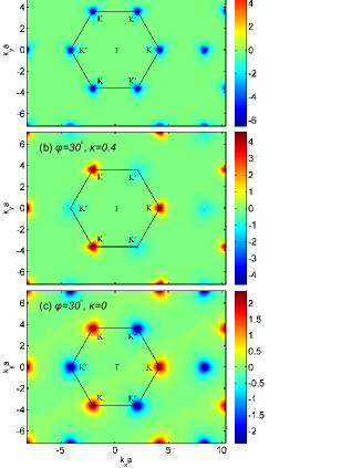
Finally, let us examine the calculated gap Berry curvature over the entire 2D BZ. Figure 5(a) shows clearly that in the case, the of the third gap has six pronounced negative peaks, respectively, at six and points, although it is rather flat with a small negative value of over the rest of the BZ. As mentioned above, these six peaks are caused by the lifting of the triply degenerate nodal points at both and points [see Fig. 3(a)] due to the replacement of the dielectric rods () by the gyromagnetic rods () which breaks the symmetry. These six peaks are identical because the distribution has the symmetry. Therefore, the integration of the gives rise to a nonzero gap Chern number of -2. Thus, the 3rd gap is a high Chern number QAH phase.
Interestingly, Figs. 5(b) and 5(c) reveal that the three negative peaks at the three points in the case become three large positive peaks in the case, caused by a simple rotation of angle from to . The in the rest of the BZ is almost zero. The distribution now has the symmetry. Consequently, the contribution from the three positive peaks at the three points to the cancels that from the three negative peaks at the points, resulting in . Interestingly, this unique pattern is identical to that in the electronic band structure of MoS2 monolayerFeng12 ; Mak14 , and thus is the signature of the QVH phase with nonzero valley Chern number of .Ma16 ; Chen17 Here is defined as the difference between two valley indices and , i.e., .Ma16 ; Chen17 The valley index () can be obtained by integrating the gap Berry curvature over half of the IBZW in the vicinity of the () point. In the case, clearly, this would give rise to and [see Fig. 5(c)], thus leading to . A further rotation of by another would make the system return to the case of , i.e., the cases of and have the same distribution [Thus, the of is not shown here]. Another rotation of by to would lead to a pattern that is identical to that of the case except a swap of and points [Thus, the of is not shown here]. However, the two valley indices would swap signs, thereby resulting in a valley Chern number of . This shows that the properties of the system as a function of has a period of .
III.4 Chiral edge states
The principle of bulk-edge correspondence guarantees that gapless one-way (chiral) edge states occur at the interface between two topologically different bulk insulators and the number of these edge states equals to the difference in the gap Chern numbers of the two insulators. (see, e.g., [joan14, ]). To further study these fascinating edge states, we calculate the edge band diagram, i.e., frequency dispersions for the wave vector along the edge of the photonic crystal for both and , as displayed in Figs. 6(a) and 6(b), respectively. In this calculation, a supercell consisting of one unit cell along the interfacial -direction [also the propagation direction ()] and 20 unit cells of [Fig. 6(a)] and [Fig. 6(a)] photonic crystals along direction with both ends terminated by a perfect electric conductor (PEC). Here the PEC is adopted to mimic a metal in the microwave region.joan08 ; skir14
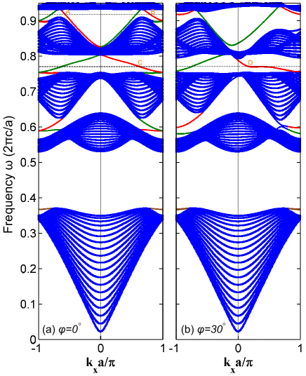
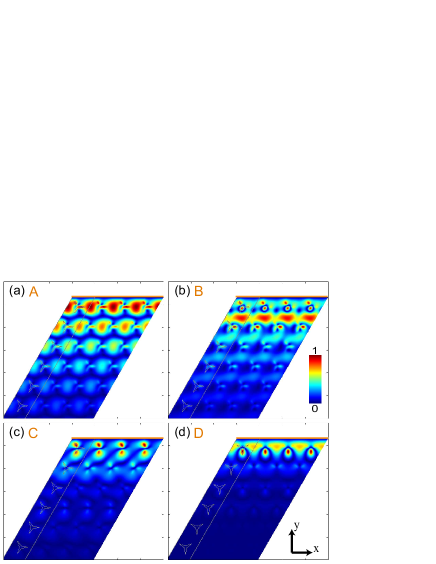
Figure 6 shows that apart from bulk projected bands (blue curves), there are one gapless edge band (red lines) in the 2nd gap region, which agree well with calculated shown in Fig. 3. Similarly, in Fig. 6(a) we can see two edge bands in the 3rd gap (). Note that the slopes of the edge bands indicate the direction of propagation (i.e., their group velocities ). In Fig. 6, the negative slopes of edge bands suggest that the waves would propagate towards the direction. On the other hand, as shown in Fig. 6(b), no gapless one-way edge band is observed in the 3rd gap, being consistent with in Fig. 3. All these observations show that bulk-edge correspondence is satisfied. Moreover, the field profiles of the edge states labelled as , , and are shown in Fig. 7. Clearly, the electric fields of edge states and from the 2nd band gap are more confined to the edge than that of the and states in the 3rd gap (Fig. 7), simply because the 2nd band gap is wider (Table I). Finally, we can also see one chiral edge band in the incomplete gap near 0.6 in Fig. 6, as can be expected from its nonzero gap Chern number of shown in Fig. 3.
III.5 Reflection immune one-way waveguides
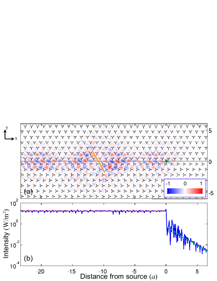
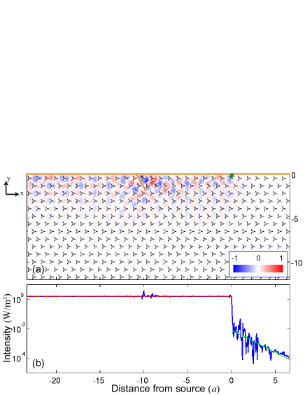
In this subsection, we should demonstrate that topologically protected one-way edge modes propagate at the interface of a Chern photonic crystal with another topologically different material by performing numerical simulations of electromagnetic (EM) wave propagations along the interface. We will also access their application potentials such as reflection free one-way waveguides. Both the second and third topological gaps of the photonic crystal [see Fig. 3(a)] will be considered. Let us first study the interface between two topological distinct photonic crystals, namely, () and (), with the source frequency in the third band gap. As illustrated in Fig. 8(a), the simulation system used consists of the crystal (lower region) and the crystal () (upper region). A point source, which radiates in all directions with frequency in the third gap, is placed at the origin (green star) in the interface. Moreover, as an obstacle to the EM wave propagation, a metallic plate (orange line) of thickness and width is inserted at -11 with the plate surface tilted away from -axis [Fig. 8(a)]. The Re field distribution displayed in Fig. 8(a) demonstrates firstly that the EM wave cannot enter the upper and lower regions because the operating frequency is in the band gap, and secondly that it cannot go right (the direction) because it is forbidden by the topological nature of the edge state. For example, the ratio (/) of the light intensity at -17 to that at 6 is . Such significant difference is the signature of unidirectionality. Therefore, the EM wave effectively can only propagate toward the direction. Furthermore, as expected, the EM wave can circumvent the metallic plate and continue traveling towards the without loss [see the calculated intensity as a function of the distance from the source in Fig. 8(b)]. In particular, the ratio of the transmitted intensities at -17 to that at -7 is 0.990, indicating that the scattering due to the obstacle (the metal plate) is minimal.
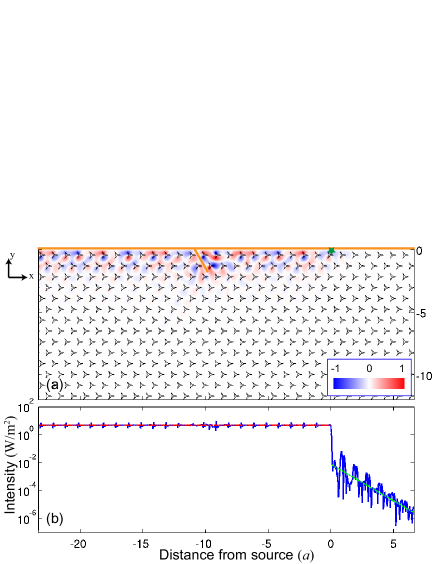
For the application as a waveguide, the surface of a photonic topolical insulator is usually covered with a metal (e.g., copper) wall. Therefore, we also perform similar simulations for the interface between the photonic crystal and a metallic wall which is topologically trivial. In principle, the larger the topological gap, the better the localization of the EM wave in the interfacial region. As a result, from the viewpoint of the application of the edge modes as one-way waveguides, it would be advantegeous to use a larger band gap. Therefore, we consider the photonic crystal with the source frequency being within the third gap (, ) and also within the second gap (, ). The calculated Re field and also the transmission intensity are displayed in Fig. 9 and Fig. 10, respectively. Indeed, Fig. 10(a) shows that the Re field is more confined to the interfacial region compared to that shown in Fig. 9. Moreover, the unidirectionality of the edge mode in the second gap is much better than that of the third gap. This is reflected in the fact that the ratio () of the wave intensity at -17 to that at 6 in Fig. 10 is nearly three orders of magnitude higher than in Fig. 9 (see Table I). Interestingly, Fig. 2 shows that the topological nature of the second gap does not depend on the rotation angle . As a result, the reflection-free one-way waveguiding would be very robust against the disorders such as the imperfect alignments of the triangular rods in the photonic crystal introduced during the waveguide fabrication processes.
The main properties of the band gaps such as the gap sizes, the gap Chern numbers (), the numbers of edge states () and on-and-off edge intensity ratio () are listed in Table. I. Firstly, Table I shows that the second gap sizes () in both and cases are large, being comparable to some well-known designs using circular rods.joan08 ; skir14 Secondly, that comfirms the bulk-edge correspondence, as mentioned before. Lastly, the large magnitudes of especially of for the second gap indicates that the waveguides made of the proposed photonic crystals would have a very high unidirectionality. This unidirectionality also manifests itself as a sharp drop in the intensity at the right-hand side of the point source towards the direction in Figs. 8-10 (b).
III.6 Valley Hall edge states and light propagation in a Z-shape bend
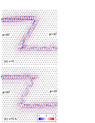
The above examination of the of the third gap over the BZ in Sec. III.3 reveals the interesting QVH phase in both (valley Chern number ) and (valley Chern number ) cases. The occurrence of this QVH phase is caused by a rotation of the triangular rods by from to . In the case where both the symmetry and the mirror symmetry exist, there are six Dirac cones of bands (Fig. 3(a), red curves) at six and points, respectively. When the system is transformed to the case, the mirror symmetry is broken and the Dirac points become gapped (Fig. 3(b), red curves), leading to nonzero Berry curvature with the odd symmetry,Niu10 i.e., [see also Fig. 5(c)]. An integration of over the BZ is zero, as required by the symmetry. As mentioned before, the case has the same pattern as that of the case except a swap of and points, i.e., the third band gap of the case is also a QVH phase but with .
Surprisingly, when symmetry is broken (i.e., ), the gap Berry phase of the third gap remains zero. The topology of bands remains unaltered and this can also be seen by comparing bands in the vicinity of the and points in Fig. 3(b) before (red curves) and after (blue curves) the introduction of the gyromagnetic material. Therefore, the third gap in the and case is also a QVH phase with . Since symmetry is now broken, the QVH phase should be called the pseudo-QVH phase, as for the pseudo-quantum spin Hall phasesChen11 ; Hsu17 . Nonetheless, the profiles of the Berry curvatures at and valleys now become different, as shown in Fig. 5(b).
It is known that the edge states in a QVH photonic topological insulator is valley-dependent and thus the intervalley scattering along the zigzag boundaryshvets13 ; Chen17 is suppressed. This would lead to valley-protected robust wave propagation in a Z-shape bend between two QVH photonic crystals with different valley Chern numbers. Therefore, to explicitly verify the QVH phases in the and crystals, we performed numerical simulations of light propagation along a Z-shape interface between these two topologically distinct crystals, as shown in Fig. 11. Figure 11(a) shows that in the case, the wave can turn around the two sharp corners, thus proving the existence of the QVH edge states at the interface. The same situation also occurs in the case [11(b)], thereby suggesting that the QVH edge states also exist in the interface between the photonic crystals. Therefore, the results of these numerical simulations indicate that the QVH photonic crystal waveguides presented here are not the ordinary photonic crystal waveguides and could have promising applications for, e.g., designng photonic valleytronic devicesMa16 .
IV conclusions
In conclusion, we have carried a comprehensive theoretical study on the topological phases in 2D photonic crystals without and symmetries. As an example, we consider a hexagonal lattice consisting of triangular gyromagnetic rods. Here the gyromagnetic material breaks invarience while the triangular rods breaks symmetry. Remarkably, we discover that the photonic crystal houses QAH phases with different gap Chern numbers () including as well as QVH phases with contrasting valley Chern numbers (). Moreover, phase transitions among these topological phases, such as from QAH to QVH and vice versa, can be realized by a simple rotation of the orientation of the rods. Our band theoretical analyses reveal that the Dirac nodes at the and valleys in the momentum space are produced and protected by the mirror symmetry () instead of the symmetry in the -invariant crystals, and they become gapped when either or symmetry is broken, leading to a QAH or QVH phase, respectively. Furthermore, the high Chern number () QAH phase arises when the rare triply degenerate nodal pointsCTCh12 ; Lu15 rather than pairs of Dirac nodesskir14 are gapped by breaking symmetry. Therefore, our proposed photonic crystal would provide a platform for exploring transitions among intriguing topological phases which may be very difficult to realize in electronic systems.
Our electromagnetic simulations of wave propagation either along the edges of our crystal capped with a metal wall or in the interfaces between two variants of our crystal with different rod orientations, demonstrate reflection-immune one-way light transports in both straight interfaces and Z-shape bends. Furthermore, we find that the second topologically nontrivial gap is not only large but also independent of the orientation of the triangular rods, and thus the topologically protected one-way wave propagation would be very robust against disorders such as misalignments of the triangular rods in the photonic crystal introduced during the fabrication processes. Therefore, our proposed crystal would also have promising potentials for device applications in photonics such as reflection-free waveguides and topological one-way circuits.
Acknowledgements.
This work is supported by the Ministry of Science and Technology, the National Center for Theoretical Sciences, Academia Sinica and the Kenda Foundation of The R.O.C.References
- (1) M. Z. Hasan and C. L. Kane, Colloquium : Topological insulators, Rev. Mod. Phys. 82, 3045 (2010).
- (2) L. Lu, J. D. Joannopoulos, and M. Soljačić, Topological photonics, Nat. Photonics 8, 821 (2014).
- (3) F. D. M. Haldane, Model for a quantum Hall effect without Landau levels: Condensed-matter realization of the ”parity anomaly”, Phys. Rev. Lett. 61, 2015 (1988).
- (4) H. M. Weng, R. Yu, X. Hu, X. Dai and Z. Fang, Quantum anomalous Hall effect and related topological electronic states, Adv. Phys. 64, 227 (2015).
- (5) C.-Z. Chang, J. Zhang, X. Feng, J. Shen, Z. Zhang, M. Guo, K. Li, Y. Qu, P. Wei, L.-L. Wang, Z.-Q. Ji, Y. Feng, S. Ji, X. Chen, J. Jia, X. Dai, Z. Fang, S.-C. Zhang, K. He, Y. Wang, L. Lu, X.-C. Ma and Q.-K., Xue, Experimental observation of the quantum anomalous Hall effect in a magnetic topological insulator, Science 340, 2573 (2013).
- (6) F. D. M. Haldane and S. Raghu, Possible realization of directional optical waveguides in photonic crystals with broken time-reversal symmetry, Phys. Rev. Lett. 100, 013904 (2008).
- (7) S. Raghu and F. D. M. Haldane, Analogs of quantum-Hall-effect edge states in photonic crystals, Phys. Rev. A 78, 033834 (2008).
- (8) Z. Wang, Y. D. Chong, J. D. Joannopoulos, and M. Soljačić, Reflection-free one-way edge modes in a gyromagnetic photonic crystal, Phys. Rev. Lett. 100, 013905 (2008).
- (9) Z. Wang, Y. Chong, J. D. Joannopoulos, and M. Soljačić, Observation of unidirectional backscattering-immune topological electromagnetic states, Nature 461, 772 (2009).
- (10) S. A. Skirlo, L. Lu, and M. Soljačić, Multimode one-way waveguides of large Chern numbers, Phys. Rev. Lett. 113, 113904 (2014).
- (11) C. He, X.-L. Chen, M.-H. Lu, X.-F. Li, W.-W. Wan, X.-S. Qian, R.-C. Yin, and Y.-F. Chen, Tunable one-way cross-waveguide splitter based on gyromagnetic photonic crystal, Appl. Phys. Lett. 96, 111111 (2010).
- (12) Z. Wang, L. Shen, Z. Yu, X. Zhang, and X. Zheng, Highly efficient photonic-crystal splitters based on one-way waveguiding, J. Opt. Soc. Am. B 30, 173 (2013).
- (13) S. A. Skirlo, L. Lu, Y. Igarashi, Q. Yan, J. Joannopoulos, and M. Soljačić, Experimental observation of large Chern numbers in photonic crystals, Phys. Rev. Lett. 115, 253901 (2015).
- (14) T. Ochiai and M. Onoda, Photonic analog of graphene model and its extension: Dirac cone, symmetry, and edge states, Phys. Rev. B 80, 155103 (2009).
- (15) W.-Y. He and C. T. Chan, The emergence of Dirac points in photonic crystals with mirror symmetry, Scientific Reports 5, 8186 (2015).
- (16) D. Xiao, M.-C. Chang, and Q. Niu, Berry phase effects on electronic properties, Rev. Mod. Phys. 82, 1959 (2010).
- (17) D. Xiao, W. Yao and Q. Niu, Valley-contrasting physics in graphene magnetic moment and topological transport, Phys. Rev. Lett. 99, 236809 (2007).
- (18) K. F. Mak, K. L. McGill, J. Park and P. L. McEuen, The valley Hall effect in MoS2 transistors, Science 344, 1489 (2014).
- (19) T. Ma and G. Shvets, All-Si valley-Hall photonic topological insulator, New J. Phys. 18, 025012 (2016).
- (20) X.-D. Chen, F.-L. Zhao, M. Chen, and J.-W. Dong, Valley-contrasting physics in all-dielectric photonic crystals: Orbital angular momentum and topological propagation, Phys. Rev. B 96, 020202 (2017).
- (21) J.-W. Dong, X.-D. Chen, H. Zhu, Y. Wang, and X. Zhang, Valley photonic crystals for control of spin and topology, Nat. Mater. 16, 298 (2017).
- (22) D. M. Pozar, Microwave Engineering, 2nd ed. (Wiley, New York, 1997).
- (23) https://www.comsol.com
- (24) T. Fukui, Y. Hatsugai, and H. Suzuki, Chern numbers in discretized Brillouin zone: Efficient method of computing (Spin) Hall Conductances, J. Phys. Soc. Jpn. 74, 1674 (2005).
- (25) Y. Hatsugai, Chern number and edge states in the integer quantum Hall effect, Phys. Rev. Lett. 71, 3697 (1993).
- (26) J. D. Joannopoulos, S. G. Johnson, J. N. Winn, and R. D. Meade, Photonic Crystals: Molding the Flow of Light, 2nd ed. (Princeton University Press, Princeton, 2008).
- (27) X. Huang, Y. Lai, Z. H. Hang, H. Zheng and C. T. Chan, Dirac cones induced by accidental degeneracy in photonic crystals and zero-refractive-index materials, Nat. Mater. 10, 582 (2011).
- (28) P. Wang, L. Lu, and K. Bertoldi, Topological phononic crystals with one-way elastic edge waves, Phys. Rev. Lett. 115, 104302 (2015).
- (29) H. Weng, C. Fang, Z. Fang, X. Dai, Topological semimetals with triply degenerate nodal points in -phase tantalum nitride, Phys. Rev. B 93, 241202 (2016).
- (30) Z. Zhu, G. W. Winkler, Q. S. Wu, J. Li and A. A. Soluyanov, Triple point topological metals, Phys. Rev. X 6, 031003 (2016).
- (31) B. Q. Lv, Z.-L. Feng, Q.-N. Xu, X. Gao, J.-Z. Ma, L.-Y. Kong, P. Richard, Y.-B. Huang, V. N. Strocov, C. Fang, H.-M. Weng, Y.-G. Shi, T. Qian and H. Ding, Observation of three-component fermions in the topological semimetal molybdenum phosphide, Nature 546, 627 (2017).
- (32) G. Y. Guo, S. Murakami, T.-W. Chen and N. Nagaosa, Intrinsic spin Hall effect in platinum: First-principles calculations, Phys. Rev. Lett. 100, 096401 (2008).
- (33) W. Feng, Y. Yao, W. Zhu, J. Zhou, W. Yao and D. Xiao, Intrinsic spin Hall effect in monolayers of group-VI dichalcogenides: A first-principles Study, Phys. Rev. B 86, 165108 (2012).
- (34) T.-W. Chen, Z.-R. Xiao, D.-W. Chiou and G.-Y. Guo, High Chern number quantum anomalous Hall phases in graphene with Haldane orbital coupling, Phys. Rev. B 84, 165453 (2011).
- (35) H.-C. Hsu, M.-J. Jhang, T.-W. Chen and G.-Y. Guo, Topological phase transitions in an inverted InAs/GaSb quantum well driven by titled magnetic fields, Phys. Rev. B 95, 195408 (2017).
- (36) A. B. Khanikaev, S. Hossein Mousavi, W.-K. Tse, M. Kargarian, A. H. MacDonald, and G. Shvets, Photonic topological insulators, Nat. Mater. 12, 233 (2013).
- (37) J. Mei, Y. Wu, C. T. Chan, and Z.-Q. Zhang, First-principles study of Dirac and Dirac-like cones in phononic and photonic crystals, Phys. Rev. B 86, 035141 (2012).