Piezoelectric field, exciton lifetime, and cathodoluminescence intensity at threading dislocations in GaN{0001}
Abstract
The strain field of a dislocation emerging at a free surface is partially relaxed to ensure stress free boundary conditions. We show that this relaxation strain at the outcrop of edge threading dislocations in GaN{0001} gives rise to a piezoelectric volume charge. The electric field produced by this charge distribution is strong enough to dissociate free excitons at distances over 100 nm from the dislocation line. We evaluate the impact of this effect on cathodoluminescence images of dislocations.
Cathodoluminescence (CL) maps of GaN{0001} surfaces reveal threading dislocations as dark spots, directly demonstrating that they act as centers of nonradiative recombination of excitons.Rosner et al. (1997); Sugahara et al. (1998); Speck and Rosner (1999); Pauc et al. (2006) The nonradiative recombination process is commonly presumed to take place at the dislocation core. The size of the dark spots, typically some 100 nm in diameter, is understood to be a result of exciton diffusion, and intensity profiles across the dislocation have been used frequently to extract quantitative information on the exciton diffusion length.Rosner et al. (1997); Sugahara et al. (1998); Speck and Rosner (1999); Shmidt et al. (2002); Nakaji et al. (2005); Pauc et al. (2006); Yakimov, Borisov, and Zaitsev (2007); Ino and Yamamoto (2008); Yakimov (2010, 2015); Sabelfeld et al. (2017)
Wurtzite GaN is a pyroelectric (and thus piezoelectric) crystal. Uniform strain produces a piezoelectric polarization, and strain variations generate a piezoelectric field that may dissociate excitons. In bulk GaN, neither -type edge nor -type screw dislocations with the line direction along cause piezoelectric fields,Smirnova (1974); Shi, Asbeck, and Yu (1999) in contrast to dislocations with other line directions. When these dislocations reach a surface, a polarization charge is created due to the discontinuity of the piezoelectric polarization as well as of the spontaneous polarization. In a previous work, this charge was presumed to be screened by free charges in surface states, and it was concluded that the piezoelectric fields of threading dislocations have a minimal effect on the electric and optical properties of GaN{0001}.Shi, Asbeck, and Yu (1999)
These considerations were based on the strain field of a straight dislocation in bulk GaN, which does not vary along the axis. However, the strain field of the dislocation changes in the vicinity of the surface to produce a stress-free boundary.Yoffe (1961); Lothe (1992) The resulting three-dimensional electric field at the dislocation outcrop in GaN{0001} was calculated numerically by a finite element approachTaupin et al. (2014) as an illustration of the computational method, but the consequences of this field were not considered.
In the present work, we calculate the distribution of the piezoelectric field that arises due to elastic strain relaxation at the surface around the outcrops of threading dislocations in GaN{0001}. This field drastically reduces the exciton lifetime close to the dislocation outcrop. We calculate the CL image of the dislocation in the absence of exciton diffusion, with exciton dissociation as the only reason for a variation of the CL signal near the dislocation. The widths of the CL intensity profiles thus obtained can approach the widths of the profiles observed experimentally.
A rigorous calculation of the piezoelectric field requires to take into account both the direct (polarization caused by strain) and the converse (stress caused by electric field) piezoelectric effects, necessitating a selfconsistent solution of the coupled equations of elasticity and electrostatics.Nye (1957); Landau and Lifshitz (1960); Auld (1973); Nowacki and Alshits (2007); Lew Yan Voon and Willatzen (2011) The relative contributions of the two effects and the need for the rigorous solution is examined in the following by order of magnitude estimates. In the next two paragraphs, the orientational dependencies and the indices of the respective tensors are omitted and the sign means “on the order of”.
The direct effect results in a polarization , where and are the characteristic magnitudes of the piezoelectric constants and the strain, respectively. The converse effect produces a stress with the electric field and the same piezoelectric constants as for the direct effect. This stress is added to the stress caused by elastic strain (here is the characteristic magnitude of the elastic moduli). As a first approximation, the electric field can be taken to be equal to that induced by the direct effect, , where is the vacuum permittivity and is the relative permittivity of GaN. Substituting this field results in a stress of , where is the electromechanical coupling constant (in a precise definition, this constant is expressed through the components of the involved tensors and depends on directions in the crystalAuld (1973)). This dimensionless quantity controls the ratio of the converse to direct piezoelectric effects. Taking for the estimate C m-2 with the elementary charge and the lattice constant , and GPa, we arrive at . This estimate agrees with the impact of the converse piezoelectric effect in planar heteroepitaxial structures.Lew Yan Voon and Willatzen (2011)
In addition to the piezoelectric effect, the spatially varying strain field of a dislocation gives rise to a polarization due to the flexoelectric effect. This effect takes place in all dielectric materials and induces a polarization (see Refs. Maranganti and Sharma, 2009; Hong and Vanderbilt, 2013; Yudin and Tagantsev, 2013 and references therein). With the characteristic magnitude of the flexoelectric constants and the dislocation strain (where is the Burgers vector and is the distance from the dislocation line), the ratio of the flexoelectric and piezoelectric effects is . Hence, at distances from the dislocation large in comparison with the atomic distances, the flexoelectric effect can be neglected.
Given the fact that the converse piezoelectric and the flexoelectric effects result in corrections of only a few percent, much less than the uncertainty introduced by the low accuracy with which the piezoelectric constants are known, we do not include them in the following calculations. In this case, the piezoelectric polarization caused by strain in a crystal with the wurtzite structure has the components
| (1) |
where , , and are the piezoelectric constants of the wurtzite structure and are the components of the strain tensor. The axis is directed along the [0001] direction. Using analytical expressions for the displacement field of an edge dislocation normal to the surfaceYoffe (1961); Lothe (1992) and calculating the corresponding components of the strain tensor, the components of the polarization vector, and the polarization charge density , we obtain
| (2) |
where and
| (3) | |||||
| (4) |
with the Poisson ratio . We restrict our calculations to the elastically isotropic case. The expressions for the displacement field of an edge dislocation far from the surface, written for an isotropic medium, remain valid for an edge dislocation in the elastically anisotropic hexagonal crystal with the dislocation line along the axis, if the Poisson ratio is taken as , where the are the elastic moduli.A. Yu. Belov (1992) With the elastic moduli of GaN,Polian, Grimsditch, and Grzegory (1996) we obtain . We use this value also for the relaxation displacement field.
For the piezoelectric constants of GaN, we take the values C m-2 and C m-2.Winkelnkemper, Schliwa, and Bimberg (2006) For we assume, as proposed in Ref. Schulz et al., 2011, . With the Burgers vector of an a-type edge dislocation nm, we obtain the values C m-1 and C m-1.
We have performed the same calculation for the charge density for a -type screw dislocation. The strain relaxation at the free surface gives rise to a non-zero piezoelectric polarization , but the charge density is equal to zero. Hence, screw threading dislocations do not generate a piezoelectric field. Since the equations of both elasticity and electrostatics are linear, mixed (-type) dislocations produce the same piezoelectric field as -type edge dislocations.
To obtain the piezoelectirc field associated with the charge density (2), we consider first the case of undoped GaN, so that free charges in the bulk are absent and the electric potential is the solution of the Poisson equation
| (5) |
We assume that the surface charges are screened by free charges, so that the boundary condition for Eq. (5) reads .
The solution of Eq. (5) for a point charge with the equipotential boundary condition is the Coulomb potential plus that of the image (of the opposite sign) with respect to the surface . Integrating the point charge solution with the charge distribution (2), we arrive at the potential
| (6) |
where and . We do not present the details of the derivation since the result can be directly verified by differentiating expression (6) and checking that Eq. (5) is satisfied with the charge density (2).
With the numerical values of the material parameters of GaN given above, we find V and . Taking , Eq. (6) simplies to
| (7) |
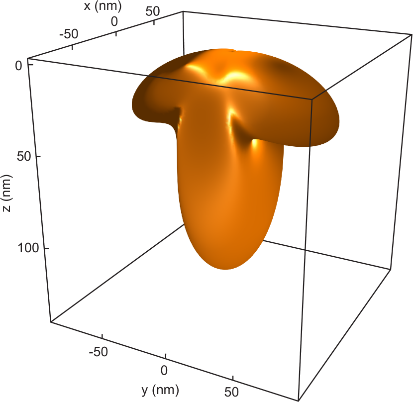
The piezoelectric field is given by . Since the exciton lifetime depends on the magnitude of the electric field rather than its direction, we visualize the field distribution in Fig. 1 by plotting an iso-field surface. The shape of this surface does not depend on and scales with its value, since . The three-dimensional surface of constant electric field at kV/cm shown in the figure extends to distances of about 70 nm from the dislocation line, and to a depth up to 140 nm from the surface.
The dissociation rate of the free exciton in the electric field is calculated analogously to the ionization probability (per unit time) of the hydrogen atom.Landau and Lifshitz (1977); Yamabe, Tachibana, and Silverstone (1977); Banavar, Coon, and Derkits, Jr. (1979) It can be expressed as
| (8) |
where the frequency and the electric field are given in terms of the exciton binding energy as and . Here is the reduced Planck constant, is the Bohr radius, is the reduced mass of the exciton (equal to 0.18 electron masses for the free A exciton in GaN). The exciton binding energy is . We thus obtain meV, s-1, and kV/cm. As an example, for the electric field kV/cm shown in Fig. 1, the characteristic dissociation time of the exciton is ns, i. e., notably smaller than the typical effective exciton lifetime in epitaxial GaN layers. Since electrons and holes are rapidly separated by the piezoelectric field, and one carrier type will be driven toward the dislocation, this process constitutes an effectively nonradiative decay channel by dissociating excitons already at distances of about 100 nm from the dislocation line. Equation (8) is derived for small electric fields such that . This condition does not restrict our considerations since, when becomes comparable with , the lifetime is so small that the dissociation process can be considered as being instantaneous.
To demonstrate the effect of the electric field displayed in Fig. 1 on exciton recombination in the absence of exciton diffusion, we calculate a CL image around an edge threading dislocation intersecting the GaN{0001} surface. Electron-hole pairs are generated by the primary electron beam with an acceleration voltage of 3 kV. The spatial distribution of these pairs, which is assumed to correspond to the distribution of free A excitons with wavevector , is obtained with the help of the free software CASINO.Drouin et al. (2007) The effective exciton lifetime including exciton dissociation by the piezoelectric field is calculated according to
| (9) |
where and are the radiative and nonradiative lifetimes far from the dislocation, respectively, and is given by Eq. (8). We take ns and ns, neglecting any dependence of these values on the electric field. The CL intensity is calculated then as a convolution
| (10) |
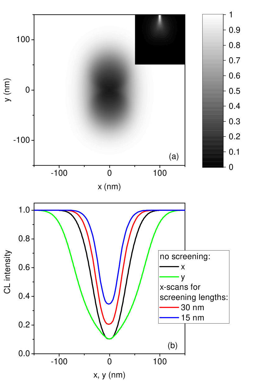
The calculated CL map and the intensity profiles along ( direction) and perpendicular to ( direction) the Burgers vector of the dislocation are presented in Figs. 2(a) and 2(b). Longer nonradiative lifetimes would produce profiles with somewhat larger width. The dependence of the width on the lifetime is, however, rather weak since sharply varies with the distance from dislocation.
The inset in Fig. 2(a) shows, on the same scale as the CL map, the spatial distribution of the electron-hole pairs generated by the electron beam. The figure shows the projection of the three-dimensional distribution on the plane. The majority of electron-hole pairs is generated in a region with a lateral width of only a few nm, so that the spatial extension of the dislocation image in Fig. 2 is entirely determined by the piezoelectric field. This width of about 100 nm is on the same order as the one observed in experimentally recorded CL images.Rosner et al. (1997); Sugahara et al. (1998); Speck and Rosner (1999); Shmidt et al. (2002); Nakaji et al. (2005); Pauc et al. (2006); Yakimov, Borisov, and Zaitsev (2007); Ino and Yamamoto (2008); Yakimov (2010, 2015); Sabelfeld et al. (2017) The image is notably extended in the direction (the direction of the extra half-plane of the dislocation). This asymmetry is expected to be smoothed out, at least partially, by diffusion of excitons.
Unintentionally doped GaN layers usually exhibit an -type background doping due to the incorporation of the shallow donors O and Si. These free electrons will screen the fields induced by the piezoelectric polarization charges. We follow the Debye-Hückel approximation for piezoelectric semiconductorsMerten (1966); Faivre and Saada (1972); Shintani (1991) and include in the Poisson equation (5) an additional free charge distribution , where is the electron density, is the Boltzmann constant and is the temperature. Then, after expansion over up to the linear term, Eq. (5) is replaced with
| (11) |
where the inverse screening length is given by . For an electron density cm-3 at room temperature, the Debye screening length is nm.
The solution of Eq. (11) for a point charge, that ensures the equipotential surface , is the screened Coulomb potential plus that of its image (of the opposite sign) with respect to the surface . To calculate the convolution integral of the charge distribution (2) with the point charge solution, we represent the charge distribution (2) as a Fourier integral
| (12) |
and arrive at the potential
This solution can be directly verified by differentiating the potential (Piezoelectric field, exciton lifetime, and cathodoluminescence intensity at threading dislocations in GaN{0001}) and checking that the screened Poisson equation (11) is satisfied with the charge distribution (12). In the limit , the potential (Piezoelectric field, exciton lifetime, and cathodoluminescence intensity at threading dislocations in GaN{0001}) reduces to Eq. (6).
Figure 2(b) shows that the screening of the piezoelectric field reduces both the width of the dislocation image and its contrast. The region of the electric field, large enough to dissociate excitons, decreases due to screening both laterally and in depth. The reduction in lateral direction results in a narrowing of the dislocation image. Its reduction in depth decreases the probability of nonradiative recombination for excitons created at larger depths and hence reduces the contrast of the dislocation image. The effect of the piezoelectric field reduces with increasing acceleration voltage of the electron beam, since the piezoelectric field is restricted in depth while the excitons are produced deeper in the crystal. Then, the nonradiative recombination at the dislocation core, along the whole dislocation line, becomes the primary mechanism of the dislocation contrast.
To summarize and conclude, the strain field of an edge threading dislocation relaxes at the surface to achieve a stress-free boundary. The resulting strain field causes an inhomogeneous distribution of piezoelectric polarization charges which, in turn, induces a volume electric field around the dislocation outcrop. Excitons dissociate in this electric field, thus reducing the exciton lifetime. Even in the absence of exciton diffusion, dislocations in undoped GaN give rise to dark spots in CL maps with diameters up to 100 nm. The Debye-Hückel screening of the piezoelectric field by free carriers reduces the image diameter. However, its width remains significant when compared to experimentally recorded CL intensity profiles of dislocations. Thus, the exciton diffusion length may be notably smaller than it is usually inferred from CL images of dislocations. We will study the effect of exciton diffusion in the presence of the piezofield at the dislocation outcrop in a forthcoming work.
The authors thank Alexander Tagantsev, Alexander Belov, and Vladimir Alshits for useful discussions and Uwe Jahn for a critical reading of the manuscript. K.K.S. acknowledges the support of the Russian Science Foundation under grant N 14-11-00083.
References
- Rosner et al. (1997) S. J. Rosner, E. C. Carr, M. J. Ludowise, G. Girolami, and H. I. Erikson, Appl. Phys. Lett. 70, 420 (1997).
- Sugahara et al. (1998) T. Sugahara, H. Sato, M. Hao, Y. Naoi, S. Kurai, S. T. K. Yamashita, K. Nishino, L. T. Romano, and S. Sakai, Jpn. J. Appl. Phys. 37, L398 (1998).
- Speck and Rosner (1999) J. S. Speck and S. J. Rosner, Physica B 273, 24 (1999).
- Pauc et al. (2006) N. Pauc, M. R. Phillips, V. Aimez, and D. Drouin, Appl. Phys. Lett. 89, 161905 (2006).
- Shmidt et al. (2002) N. M. Shmidt, O. A. Soltanovich, A. S. Usikov, E. B. Yakimov, and E. E. Zavarin, J. Phys.: Condens. Matter 14, 13285 (2002).
- Nakaji et al. (2005) D. Nakaji, V. Grillo, N. Yamamoto, and T. Mukai, J. Electron Microscopy 54, 223 (2005).
- Yakimov, Borisov, and Zaitsev (2007) E. B. Yakimov, S. S. Borisov, and S. I. Zaitsev, Semiconductors 41, 411 (2007).
- Ino and Yamamoto (2008) N. Ino and N. Yamamoto, Appl. Phys. Lett. 93, 232103 (2008).
- Yakimov (2010) E. B. Yakimov, Appl. Phys. Lett. 97, 166101 (2010).
- Yakimov (2015) E. B. Yakimov, J. Alloys Compounds 627, 344 (2015).
- Sabelfeld et al. (2017) K. K. Sabelfeld, V. M. Kaganer, C. Pfüller, and O. Brandt, J. Phys. D: Appl. Phys. 50, 405101 (2017).
- Smirnova (1974) I. S. Smirnova, Sov. Phys. – Solid State 15, 1543 (1974).
- Shi, Asbeck, and Yu (1999) C. Shi, P. M. Asbeck, and E. T. Yu, Appl. Phys. Lett. 74, 573 (1999).
- Yoffe (1961) E. H. Yoffe, Philos. Mag. 6, 1147 (1961).
- Lothe (1992) J. Lothe, in Elastic Strain Fields and Dislocation Mobility, edited by V. L. Indenbom and J. Lothe (North-Holland, Amsterdam, 1992) Chap. 5, sec. 6.3.
- Taupin et al. (2014) V. Taupin, C. Fressengeas, P. Ventura, M. Lebyodkin, and V. Gornakov, J. Appl. Phys. 115, 144902 (2014).
- Nye (1957) J. F. Nye, Physical Properties of Crystals (Clarendon Press, Oxford, 1957).
- Landau and Lifshitz (1960) L. D. Landau and E. M. Lifshitz, Electrodynamics of Continuous Media (Pergamon Press, London, U.K., 1960).
- Auld (1973) B. A. Auld, Acoustic Fields and Waves in Solids, Vol. I (Wiley, N.Y., 1973) Chap. 8.
- Nowacki and Alshits (2007) J. P. Nowacki and V. I. Alshits, in Dislocations in Solids, Vol. 13, edited by F. R. N. Nabarro and J. P. Hirth (Elsevier, Amsterdam, 2007) Chap. 72, pp. 47–79.
- Lew Yan Voon and Willatzen (2011) L. C. Lew Yan Voon and M. Willatzen, J. Appl. Phys. 109, 031101 (2011).
- Maranganti and Sharma (2009) R. Maranganti and P. Sharma, Phys. Rev. B 80, 054109 (2009).
- Hong and Vanderbilt (2013) J. Hong and D. Vanderbilt, Phys. Rev. B 88, 174107 (2013).
- Yudin and Tagantsev (2013) P. V. Yudin and A. K. Tagantsev, Nanotechnology 24, 432001 (2013).
- A. Yu. Belov (1992) A. Yu. Belov, in Elastic Strain Fields and Dislocation Mobility, edited by V. L. Indenbom and J. Lothe (North-Holland, Amsterdam, 1992) Chap. 6, sec. 2.5.
- Polian, Grimsditch, and Grzegory (1996) A. Polian, M. Grimsditch, and I. Grzegory, J. Appl. Phys. 79, 3343 (1996).
- Winkelnkemper, Schliwa, and Bimberg (2006) M. Winkelnkemper, A. Schliwa, and D. Bimberg, Phys. Rev. B 74, 155322 (2006).
- Schulz et al. (2011) S. Schulz, M. A. Caro, E. P. O’Reilly, and O. Marquardt, Phys. Rev. B 84, 125312 (2011).
- Landau and Lifshitz (1977) L. D. Landau and E. M. Lifshitz, Quantum Mechanics (Pergamon Press, Oxford, UK, 1977) §77, problem 1.
- Yamabe, Tachibana, and Silverstone (1977) T. Yamabe, A. Tachibana, and H. J. Silverstone, Phys. Rev. A 16, 877 (1977).
- Banavar, Coon, and Derkits, Jr. (1979) J. R. Banavar, D. D. Coon, and G. E. Derkits, Jr., Appl. Phys. Lett. 34, 94 (1979).
- Drouin et al. (2007) D. Drouin, A. R. Couture, D. Joly, X. Tastet, and V. Aimez, Scanning 29, 92 (2007).
- Merten (1966) L. Merten, Z. Naturforsch. A 21, 793 (1966).
- Faivre and Saada (1972) G. Faivre and G. Saada, Phys. Stat. Sol. B 52, 127 (1972).
- Shintani (1991) K. Shintani, J. Appl. Phys. 69, 8119 (1991).