Visualization of electronic topology in ZrSiSe by scanning tunneling microscopy
Abstract
As emerging topological nodal-line semimetals, the family of ZrSiX (X = O, S, Se, Te) has attracted broad interests in condensed matter physics due to their future applications in spintonics. Here, we apply a scanning tunneling microscopy (STM) to study the structural symmetry and electronic topology of ZrSiSe. The glide mirror symmetry is verified by quantifying the lattice structure of the ZrSe bilayer based on bias selective topographies. The quasiparticle interference analysis is used to identify the band structure of ZrSiSe. The nodal line is experimentally determined at 250 meV above the Fermi level. An extra surface state Dirac point at 400 meV below the Fermi level is also determined. Our STM measurement provides a direct experimental evidence of the nodal-line state in the family of ZrSiX.
The topology of electronic bands is closely correlated with intrinsic symmetries in topological materials chiu2016classification . The three dimensional (3D) Dirac semimetals host a fourfold degenerate Dirac point, which is protected by spatial inversion symmetry, time reversal symmetry and additional threefold or fourfold rotational symmetry along the -axis liu2014discovery ; wang2012dirac . If one symmetry is broken, the spin-doublet degeneracy of the bands is removed and the Dirac point is changed to the twofold degenerate Weyl point, leading to a Weyl semimetal weng2015weyl ; lv2015experimental ; xu2015discovery ; inoue2016quasiparticle . In contrast, the topological nodal-line semimetals host a loop of Dirac points in the momentum space, which has recently been predicted theoretically and verified experimentally xu2015two ; bian2016topological ; hu2016evidence . The formation of a nodal line requires extra symmetries, such as mirror reflection symmetry bian2016topological or glide mirror symmetry xu2015two . The appearance of Dirac or Weyl points near the Ferimi level gives rise to exotic electronic properties, such as large magnetoresistance ali2016butterfly ; wang2016evidence ; lv2016extremely ; singha2017large , high carrier density hu2017nearly and mobility wang2016evidence ; ali2016butterfly ; sankar2017crystal . The nodal-line semimetals are thus good candidates of spintronics for both fundamental research and future applications.
In a previous study, a nodal line was observed in the band structure of PaTaSe2 bian2016topological . Due to interference of other bands, the investigation of nodal-line Dirac fermions is difficult around the Fermi level. In a different family of ZrSiX (X = O, S, Se, Te) semimetals with glide mirror symmetry, the nodal line is theoretically predicted xu2015two . The calculation shows that the Dirac cone is linearly dispersed in a large energy range ( 2 eV), without interference of other bands. Through the measurement of the band structure below the Fermi level, angle-resolved photoemission spectroscopy (ARPES) has probed the linear band dispersions of ZrSiS and ZrSiSe schoop2016dirac ; neupane2016observation ; hosen2017tunability . However, the theoretical prediction of the nodal line is above the Fermi level so that ARPES cannot make a direct measurement. Instead, scanning tunneling microscope (STM) is a powerful tool to detect both the topography and local density of states (LDOS), which provides a transparent view of microscopic properties. A quasiparticle interference (QPI) technique can be used to extract the band structure in a broad energy above and below the Fermi level hoffman2002imaging . The previous STM measurements on ZrSiS however did not really determine the nodal-line state due to their limitations in data acquisition and analysis lodge2017observation ; butler2017quasiparticle .
In this paper, we take the STM measurement on ZrSiSe. Our study resolves a bias selective topography and precisely identifies an atomic shift between Zr and Se sublattices, giving an evidence of the glide mirror symmetry in ZrSiSe. The QPI analysis visualizes the linear band dispersion, which determines a nodal line located at meV above the Fermi level and a Dirac point located at meV below the Fermi level. Our measurement is thus the first STM determination of the nodal-line state in the family of ZrSiX.
High-quality single crystals of ZrSiSe in our experiment are grown by the chemical vapor transport method. STM measurements are carried out in a commercial ultra-high vacuum system zheng2017study . The samples are cleaved in situ at liquid nitrogen temperature and immediately inserted into the STM head. An electrochemically etched tungsten tip is treated with the field emission on a single crystalline of Au(111) surface. All data are acquired at liquid helium temperature ( 4.5 K).
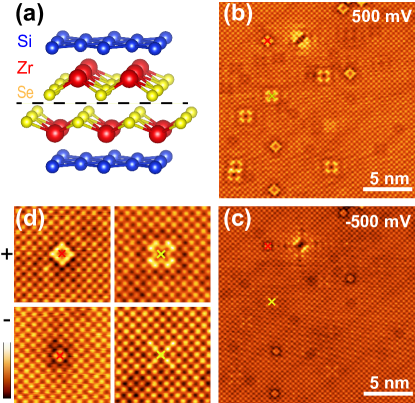
The crystal structure of ZrSiSe is in the space group of 4/ xu2015two . As shown in Fig. 1(a), each Si square layer is sandwiched by two sets of ZrSe bilayers. The crystal is cleaved in between two adjacent ZrSe bilayers and a Se square layer is exposed to be the surface plane. Figures 1(b) and 1(c) display topographies under two opposite bias voltages in the same field of view (FOV). The detected lattice is shifted from the top to hollow sites when the bias voltage is switched. As an illustration, we present enlarged images of two defects in Fig. 1(d). Under the positive bias voltage [Fig. 1(d), upper panels], the centers of the diamond and cross shaped defects are at the top and hollow sites, respectively. Under the negative bias voltage [Fig. 1(d), lower panels], these two centers are switched to their opposite sites. Two different sublattices are detected in the STM, each selected by a specific bias voltage polarity.
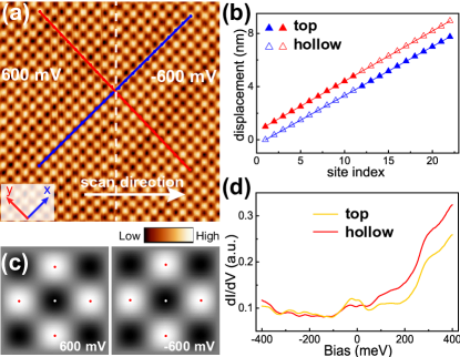
To further explore the atomic structure of ZrSiSe, we perform a designed experiment on a clean surface. As shown in Fig. 2(a), the topography is scanned along the left-to-right direction. The applied bias voltage is initially positive and suddenly switched to a negative value at an intermediate position [Fig. 2(a), dashed line]. With respect to this switching line, the left and right topographies are shifted due to the change of the bias voltage. Two linecuts (blue and red) along the - and -directions are selected as a demonstration. The red line crosses the top sites under the positive bias and then the hollow sites under the negative bias. In Fig. 2(b), we record the sequence of these sites and plot their relative displacements, which are in a perfect linear relation with the site index. The same behavior is observed for the sites along the blue line. The hollow sites under the negative bias are thus extended from the top sites under the positive bias, and vice versa.
For each of the left and right topographies, a ‘supercell’ technique lawler2010intra ; fujita2014simultaneous ; zeljkovic2015dirac is applied to extract an averaged image with a significantly reduced error. The (, ) spatial displacement with the lattice constant 3.62 Å is precisely determined between neighboring top and hollow sites for both topographies [Fig. 2(c)]. Under a given bias voltage, the top and hollow sites form two different sublattices, attributed to two planes of the ZrSe bilayer. To identify their components, we average the spectra over the top and hollow sites separately. The local density of unoccupied states at the hollow sites is consistently larger than that at the top sites [Fig. 2(d)]. The 5 orbitals of Zr atoms are highly unoccupied while the 4 orbitals of Se atoms are highly filled. Thus, the sublattices of the top and hollow sites with the negative bias correspond to the Se and Zr layers, respectively. The opposite result can be obtained for the positive bias. Our topography measurement visualizes the atomically resolved structure of the ZrSe bilayer, which obeys a key requirement of the glide mirror symmetry in ZrSiSe.
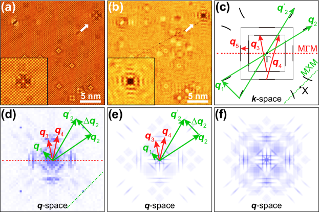
The Fourier transformed scanning tunneling spectroscopy (FT-STS) is next employed to detect the electronic topology of ZrSiSe, which is resulted directly from its structural symmetry. With a bias voltage of 500 mV, the topography of a new FOV is displayed in Fig. 3(a), in which a specific cross-shaped impurity is found on the top right corner. The conductance map simultaneously taken under the same bias voltage is drawn in Fig. 3(b). This specific cross-shaped impurity induces a strong elastic scattering, which mixes the electronic eigenstates of different wavevectors ( and ) but the same energy. The QPI is signalled by a standing wave in the LDOS around the impurity, as shown by an enlarged image in the inset of Fig. 3(b). The Fourier transform of this local conductance map is drawn in Fig. 3(d). The QPI patterns in the momentum -space can be used to identify the wavevector difference before and after the elastic scattering (), which helps building the contour of constant energy (CCE). As shown in Fig. 3(d), the centrally symmetric QPI patterns can be mainly partitioned into three groups: a diamond, two concentric squares, and four sets of triplet lines. For these pattern groups, we assign their typical scattering wavevectors, labelled from to in different colors. Other QPI patterns cannot be ruled out due to the resolution of our FT-STS map. In addition, the structure of QPI patterns changes with the scattering impurity and more discussions are provided in Supplementary Materials.
To interpret the three groups of QPI patterns, we propose a model CCE with two groups of patterns in Fig. 3(c). The first group includes four pairs of short arcs around four X points, contributing to the diamond () and triplet ( and ) QPI patterns. The diamond pattern results from scattering between the arcs of the same pair, while the triplet pattern results from scattering between the arcs at the diagonal corners. The second group consists of two concentric squares of , contributing to the concentric squares of the QPI patterns ( and ). The two groups of CCE patterns are similar to those observed in ARPES hosen2017tunability . However, a key difference is that only the occupied states below the Fermi level are detected in ARPES. To reproduce the experimental QPI patterns, we introduce a selection rule that the elastic scattering only occurs between the CCE patterns of the same group. The physical mechanism behind this selection rule is that the two CCE groups belong to the surface and bulk bands separately schoop2016dirac . The QPI map calculated based on the CCE model and the selection rule [Fig. 3(e)] shares the same major features as those from the experimental measurement [Fig. 3(d)]. As a comparison, the calculation without the selection rule [Fig. 3(f)] clearly deviates from the experimental result.
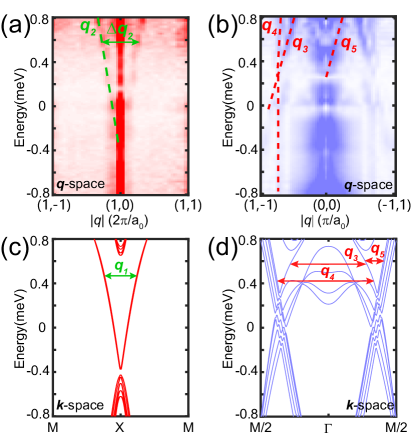
Next we measure the energy dependent conductance maps around this impurity and study the energy dispersion relations. Figure 4(a) presents the result of along the green line in the -space [Fig. 3(d)]. The triplet QPI pattern [Fig. 3(d)] is gradually compressed as the energy approaches the Fermi level from above. A linear energy dispersion of the scattering wavevectors, and , is observed. Their difference, , vanishes roughly at the bias voltage of mV, indicating a Dirac cone in the electronic band structure. Due to the scattering within the same CCE group, a simple relation, , holds. The energy dispersion of (not shown) follows the same behavior of , further confirming the existence of the Dirac cone. In Fig. 4(c), we provide the density functional theory (DFT) calculation of the slab band structure along the M-X-M direction in the -space. The predicted Dirac point, if ignoring the small gap due to the spin-orbital coupling (SOC), is consistent with our experimental measurement. In addition, this Dirac cone is a surface derived state since it is not observed in the DFT calculation of the bulk ZrSiSe.
Figure 4(b) presents the result of along the red line in the -space [Fig. 3(d)]. As the energy approaches the Fermi level from above, the sizes of the two concentric QPI squares [Fig. 3(d)] are both enlarged, but with different speeds. These two squares are merged into a single square, indicating the appearance of a nodal line. The linear energy dispersion is also found for the scattering wavevectors, and . As the amplitude of is increased fast than that of , the crossing point of these two wavevectors leads to an estimation of the nodal line at the energy of meV above the Fermi level. In our CCE model, arises from the scattering within the inner square, while arises from the scattering between the two opposite sides of the inner and outer squares [Fig. 3(c)]. A possibility causing the change of the and is that the inner square is expanded and the outer square is shrunk with the decrease of energy. In Fig. 4(d), we present the DFT calculation of the slab band structure along the M--M direction in the -space. The above conjecture of the dispersion relation of the two bands is confirmed theoretically. In addition to and , another scattering wavevector is also observed due to the scattering between the same sides of the inner and outer CCE squares [Fig. 3(c)]. The dispersion relation of [Fig. 4(b)] confirms the nodal line at the same energy level as that estimated from the mergence of and . Compared to the surface derived Dirac point at the X point, this nodal line is attributed to the bulk band structure, as shown by the DFT calculation. An interesting phenomenon is that the QPI pattern due to the scattering within the outer CCE square is missing, which is possibly due to the impurity sensitivity on the band scattering.
In summary, we perform a sophisticated STM experiment on a novel 3D topological semimetal, ZrSiSe. The bias selective topographies allow us to identify the lattice structure of the ZrSe bilayer with a sub-atomic resolution, which confirms the glide mirror symmetry in ZrSiSe. The QPI technique in the FT-STS measurement is further applied to extract the electronic structure of ZrSiSe. By analyzing QPI patterns with assistance of the CCE model and DFT calculation, we determine the nodal line in the bulk band, at 250 meV above the Fermi level. In addition, a Dirac point is also determined at 400 meV below the Fermi level. Compared to an indirect determination in previous ARPES studies, our STM measurement directly visualizes the topological nodal-line state in ZrSiSe. This method can be generalized to other nodal-line semimetals in the same family, including two dimensional films.
Acknowledgements.
This work was supported by the National Basic Research Program of China (2014CB921203 and 2015CB921004), the National Natural Science Foundation of China (NSFC-11374260), and the Fundamental Research Funds for the Central Universities in China. F.C., X.L. and Y.S. thank the support of the National Key Research and Development Program (2016YFA0300404) and the National Nature Science Foundation of China (NSFC-11674326) and the Joint Funds of the National Natural Science Foundation of China and the Chinese Academy of Sciences’ Large-Scale Scientific Facility (U1432139). K.B. and Y.F. contribute equally to this work.References
- (1) C.-K. Chiu, J. C. Y. Teo, A. P. Schnyder, and S. Ryu, Rev. Mod. Phys. 88, 035005 (2016).
- (2) Z. J. Wang, Y. Sun, X.-Q. Chen, C. Franchini, G. Xu, H. M. Weng, X. Dai, and Z. Fang, Phys. Rev. B 85, 195320 (2012).
- (3) Z. K. Liu, B. Zhou, Y. Zhang, Z. J. Wang, H. Weng, D. Prabhakaran, S.-K. Mo, Z.-X. Shen, Z. Fang, X. Dai, Z. Hussain, and Y. L. Chen, Science 343, 864 (2014).
- (4) H. M. Weng, C. Fang, Z. Fang, B. A. Bernevig, and X. Dai, Phys. Rev. X 5, 011029 (2015).
- (5) B. Q. Lv, H. M. Weng, B. B. Fu, X. P. Wang, H. Miao, J. Ma, P. Richard, X. C. Huang, L. X. Zhao, G. F. Chen, Z. Fang, X. Dai, T. Qian, and H. Ding, Phys. Rev. X 5, 031013 (2015).
- (6) S.-Y. Xu, I. Belopolski, N. Alidoust, M. Neupane, G. Bian, C.L. Zhang, R. Sankar, G. Q. Chang, Z. J. Yuan, C.-C. Lee, S.-M. Huang, H. Zheng, J. Ma, D. S. Sanchez, B. K. Wang, A. Bansil, F. C. Chou, P. P. Shibayev, H. Lin, S. Jia, and M. Z. Hasan, Science 349, 613–617 (2015).
- (7) H. Inoue, A. Gyenis, Z. J. Wang, J. Li, S. W. Oh, S. Jiang, N. Ni, B. A. Bernevig, and A. Yazdani, AAAS 351, 1184–1187 (2016).
- (8) G. Bian, T.-R. Chang, R. Sankar, S.-Y. Xu, H. Zheng, T. Neupert, C.-K. Chiu, S.-M. Huang, G. Chang, I. Belopolski, D. S. Sanchez, M. Neupane, C. Liu, B. Wang, C.-C. Lee, H.-T. Jeng, C. Zhang, Z. Yuan, S. Jia, A. Bansil, F. Chou, H. Lin, and M. Z. Hasan, Nat. Commun. 7, 10556 (2016).
- (9) Q. Xu, Z. Song, S. Nie, H. Weng, Z. Fang, and X. Dai, Phys. Rev. B 92, 205310 (2015).
- (10) J. Hu, Z. J. Tang, J. Y. Liu, X. Liu, Y. L. Zhu, D. Graf, K. Myhro, S. Tran, C. N. Lau, J. Wei, and Z. Q. Mao, Phys. Rev. Lett. 117, 016602 (2016).
- (11) M. N. Ali, L. M. Schoop, C. Garg, J. M. Lippmann, R. Lara, B. Lotsch, and S. S. P. Parkin, Sci. Adv. 2, e1601742 (2016).
- (12) X. F. Wang, X. C. Pan, M. Gao, J. H. Yu, J. Jiang, J. R. Zhang, H. K. Zuo, M. H. Zhang, Z. X. Wei, W. Niu, Z. C. Xia, X. G. Wan, Y. L. Chen, F. Q. Song, Y. B. Xu, B. G. Wang, G. H. Wang, and R. Zhang, Adv. Electron. Mater. 2, (2016).
- (13) Y.-Y. Lv, B.-B. Zhang, X. Li, S.-H. Yao, Y. B. Chen, J. Zhou, S.-T. Zhang, M.-H. Lu, and Y.-F. Chen, Appl. Phys. Lett. 108, 244101 (2016).
- (14) R. Singha, A. K. Pariari, B. Satpati, and P. Mandal, Proc. Natl. Acad. Sci. 114, 2468 (2017).
- (15) J. Hu, Z. J. Tang, J. Y. Liu, Y. L. Zhu, J. Wei, and Z. Q. Mao, Phys. Rev. B 96, 045127 (2017).
- (16) R. Sankar, G. Peramaiyan, I. P. Muthuselvam, C. J. Butler, K. Dimitri, M. Neupane, G. N. Rao, M.-T. Lin, and F. C. Chou, Sci. Rep. 7, 40603 (2017).
- (17) L. M. Schoop, M. N. Ali, C. Straßer, A. Topp, A. Varykhalov, D. Marchenko, V. Duppel, S. S. P. Stuart, B. V. Lotsch, and C. R. Ast, Nat. Commun. 7, (2016).
- (18) M. Neupane, I. Belopolski, M. M. Hosen, D. S. Sanchez, R. Sankar, M. Szlawska, S.-Y. Xu, K. Dimitri, N. Dhakal, P. Maldonado, P. M. Oppeneer, D. Kaczorowski, F.-C. Chou, M. Z. Hasan, and T. Durakiewicz, Phys. Rev. B 93, 201104 (2016).
- (19) M. M. Hosen, K. Dimitri, I. Belopolski, P. Maldonado, R. Sankar, N. Dhakal, G. Dhakal, T. Cole, P. M. Oppeneer, D. Kaczorowski, F.-C. Chou, M. Z. Hasan, T. Durakiewicz, and M. Neupane, Phys. Rev. B 95, 161101 (2017).
- (20) J. E. Hoffman, K. McElroy, D.-H. Lee, K. M. Lang, H. Eisaki, S. Uchida, and J. C. Davis, Science 297, 1148 (2002).
- (21) C. J. Butler, Y.-M. Wu, C.-R. Hsing, Y. Tseng, R. Sankar, C.-M. Wei, F.-C. Chou, and M.-T. Lin, Phys. Rev. B 96, 195125 (2017).
- (22) M. S. Lodge, G. Chang, C. Y. Huang, B. Singh, J. Hellerstedt, M. T. Edmonds, D. Kaczorowski, M. M. Hosen, M. Neupane, H. Lin, M. S. Fuhrer, B. Weber, and M. Ishigami, Nano. Lett. 17, 7213 (2017).
- (23) Y. Zheng, Y. Fei, K. L. Bu, W. H. Zhang, Y. Ding, X. J. Zhou, J. E. Hoffman, and Y. Yin, Sci. Rep. 7, 8059 (2017).
- (24) M. J. Lawler, K. Fujita, J. Lee, A. R. Schmidt, Y. Kohsaka, C. K. Kim, H. Eisaki, S. Uchida, J. C. Davis, J. P. Sethna, and E.-A. Kim, Nature 466, 347 (2010).
- (25) K. Fujita, C. K. Kim, I. Lee, J. Lee, M. H. Hamidian, I. A. Firmo, S. Mukhopadhyay, H. Eisaki, S. Uchida, M. J. Lawler, E.-A. Kim, and J. C. Davis, Science 344, 612 (2014).
- (26) I. Zeljkovic, Y. Okada, M. Serbyn, R. Sankar, W. Raman, D. Walkup, W. Zhou, J. Liu, G. Chang, Y. J. Wang, M. Z. Hasan, F. C. Chou, H. Lin, A. Bansil, L. Fu, and V. Madhavan, Nat. Mater. 14, 318 (2015).