Characterizing Germanium Junction Transistors
Abstract
Transistors have provided the basis of modern electronics. Being relatively intricate devices, and often exhibiting intense parameter variation, this type of electronic devices has motivated much research interest especially regarding their characterization and modeling. In this work, we apply a recently reported modeling methodology, based on the Early effect, for characterizing new old stock NPN and PNP small signal germanium junction transistors and comparing them to more modern silicon bipolar junction devices. The Early approach is special in the sense that its two parameters, namely the Early voltage and a proportionality parameter , are fixed and independent of transistor operation. Remarkable results are obtained, including the fact that the four considered groups, namely NPN and PNP germanium and silicon devices, occupy mostly non-overlapping regions in the Early parameter space, with PNP devices presenting larger parameter variability in both cases. Surprisingly, the considered germanium devices exhibited smaller parameter variability than observed for the silicon counterparts. When mapped into the more traditional space defined by the current gain and output resistance parameters, the four transistor groups exhibited much larger overlaps and yielded a clustering structure much less organized than allowed by the Early mapping. This result suggest that the Early representation of transistors is more compatible and inherently related to the structure of amplifying devices such as those considered in this work. In addition, it was verified that the center of mass of each of the NPN-PNP pairs of germanium and silicon devices are crossed by respective -isolines for gains of 130 and 250, respectively. Germanium devices were also characterized as having smaller output resistance and smaller magnitudes of Early voltage.
“The only thing we know about the future is that it will be different.”
Peter F. Drucker
I Introduction
It is not so often realized that most of modernity has been supported, and to some extent even defined, by electronics. Though the analogue is frequently said about computing, this important area itself relies strongly on electronics. As the development of modern electronics started with the transistor invention in 1947 riordan:1997 , the above sentence could be rephrased as modernity, ultimately, being induced by the transistor. As a matter of fact, any cell phone or personal computer, not to say the myriad of other electronic devices and systems that permeate our lives, rely critically on millions of transistors – it remains an interesting question to estimate the number of transistors involved in the Internet. Though most of these devices employ silicon as basic semiconductor material, the first transistors employed germanium, which was dominant from 1947 to the mid 50’s riordan:1997 and used until the 60’s and even 70’s. While MOSFET technology mostly predominates in modern analog electronics, point contact, grown junction, alloy junction and surface barrier were employed from 1947 to mid 50’s.
Both germanium (Ge) and silicon (Si) are semiconductor materials, characterized by increase of conductivity with temperature as free carriers are transferred from the valence to the conduction bands (e.g. parker:2004 ; sze:1969 ; jones:1995 ). However, as summarized in Table 1, these two semiconductor materials have quite distinct physical and electronic properties. In particular, the substantially larger mobility of germanium has great influence on the electronic properties of respectively derived transistors. Though this would represent, in principle, an advantage for germanium devices, there are some shortcomings potentially constraining the electronic applications of these devices relatively to silicon counterparts. These include the fact that more free electrons are available at room temperature in germanium than in silicon, implying considerably smaller current cut-off () for silicon devices. Germanium-based transistors are also characterized by smaller peak inverse voltage () than silicon devices, averaging and , respectively. In addition, the typical working temperature for germanium is only about for germanium, being much larger (about ) for silicon. Such issues contributed to the progressive shift from germanium to silicon as the basic semiconductor material adopted for industrialized transistors.
| Property | Silicon | Germanium |
|---|---|---|
| Electron mobility | 1500 | 3900 |
| Hole mobility | 470 | 1900 |
| Electron effective mass | 300 | 500 |
| Band gap | 1.1 | 0.67 |
| Dielectric constant | 11.9 | 16.0 |
| Melting point | 1415 | 937 |
| 2 | ||
| 1000 | 350 | |
| Typical working temperature | 160 | 70 |
Except for , the germanium relative limitations are more critical only for given applications and circumstances, remaining a viable choice for many important usages, such as in many small signal and low power linear circuits, especially when special attention is given to temperature management and circuit design. So, germanium remains a potentially interesting choice in transistor electronics. Some important issues that could impact on the eventual use of germanium devices in linear electronics concern their electronic parameters (e.g. stewart:1956 ; jaeger:1997 ; sedra:1998 ; boylestad:2008 ; jaeger:1997 ), such as the current gain and output resistance , as well as frequency features such as . Relatively little can be found in the literature regarding the more systematic characterization of real-world germanium devices. Actually, even the available data is often of relatively limited assistance because both and tend to vary largely with and during normal circuit operation, while the given parameter values are typically limited to averages or specific to given operation points. A substantially more comprehensive characterization of the electronic properties of a transistor can be achieved by considering the whole region of operation in the characteristic space, where and stand for the collector voltage and current, respectively. In addition, even when taken from the very same lot, transistors tend to present largely varying parameters, implying several devices to be considered so as to achieve statistical significance.
The fact that germanium transistors have some potentially interesting physical features, especially higher mobilities, while their other limitations do not completely undermine their applications in many practical circuits and circumstances, entails the interesting prospect of verifying, in a more systematic and comprehensive way, how germanium transistors behave electronically. In particular, it would be interesting to compare small signal germanium and silicon devices, so as to try to identify their respective relative main pros and cons. These issues motivate the present work. This is a timely endeavor because, with the with the advances in instrumentation and information technology, more systematic, stable and comprehensive approaches to transistor characterization have become available. In particular, we resource to the Early effect-related method reported in costaearly:2017 ; costaearly:2018 , as well as the systematic approach to characterization of transistors described in costafeed:2017 .
The application of these methodologies, while considering new old stock germanium junction transistors, led to several remarkable results, which are presented and discussed in this work. Of particular relevance is the fact that the distribution of the devices resulted much more definite and organized than that obtained in the more traditional and electronically intuitive space defined by the current gain and the collector, or output resistance . This important result paves the way to more systematic characterization studies aimed at mapping several types of amplifying devices in the Early space, so as to assist the analysis and design of electronic devices and circuits.
This article starts by revising the theoretic-experimental-numeric Early characterization approach costaearly:2017 ; costaearly:2018 and proceeds by presenting and discussing the results obtained with respect to three types of germanium junction transistors as well as a comparison with results previously costaearly:2018 obtained for 7 complementary types of silicon transistors.
II Early Modeling and Characterization
In 1952, an interesting electronic effect taking place in junction semiconductors was reported by J. M. Early, in which the width of the charge carrier portion of the base varies with the base-collector voltage. In typical transistor configurations, this implies that, for a fixed current base , the collector voltage will not be zero for , but rather would take a negative value (the Early voltage), were it possible to cross over to negative values of . This is illustrated in Figure 1, which also shows the chosen region of operation (defined by and ) and the load line defined by a chosen load resistance L and considering a simplified common emitter configuration in which the load is attached between the voltage supply and the collector. It should be taken into account that, for simplicity’s sake, all voltages and currents for the PNP devices are taken in absolute values in this work.
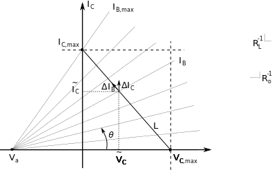
The angle has been experimentally found costaearly:2017 ; costaearly:2018 , at least for the devices considered in that work, to be directly proportional to the base current, i.e. . The Early voltage and the proportionality parameter constitute the two parameters of the Early modeling. This linear relationship turns out to be of great importance for deriving and applying the Early model, as it considerably simplifies the respective calculations and contributes to the simplicity of the approach and for the derivation of several analytical relationships. Observe that the Early model is also special in the sense that its two just mentioned parameters do not vary with either or , as it happens with the large majority of the more traditionally adopted junction transistors models. The more commonly adopted parameters known as current gain () and output resistance (), also illustrated in Figure 1, are defined (e.g. stewart:1956 respectively as:
| (1) | |||
| (2) |
In this more traditional parametrization, we have that both and are functions of the two collector variables, i.e. and . So, at a given point , needs to be approximated as , while (and ) remains constant along the whole space. Still, and are also required, because they correspond to more intuitive electronic properties of the transistors. Fortunately, it is possible to derive relationships costaearly:2018 between the Early parameters and the values of and , both averaged along the region of operation and , which are given costaearly:2018 as
| (3) | |||
| (4) |
where is the maximum collector voltage considered (in this work, ), is the minimum collector current needed to be taken into account so as to avoid divergence in Equation 4 (here, ), and is the maximum considered collector voltage (henceforth taken as ). In this way, the relative advantages of the two parametrizations can be combined.
The Early parameters and of a real-world transistor can be numerically estimated by applying the following three steps costaearly:2017 ; costaearly:2018 : (i) the values of , , and are obtained experimentally by scanning the device with a succession of values (note that other schemes can be used); (ii) a Hough transform accumulation (or voting) scheme is employed to identify the point in the space where the isolines (obtained by linear regression) intercept, leading to the estimation of ; and (iii) linear regression is applied in order to obtain from the parameters and , the latter corresponding to the tangent of the angular coefficient of the respective isolines.
The above outlined methodology has been applied with encouraging success for the experimental characterization of BJT NPN-PNP complementary pairs costaearly:2018 , yielding several interesting results including the identification of two almost non-overlapping groups defined respectively by these two types of devices, each with well-defined specific electronic properties. In addition, all the considered devices were found to populate a relatively narrow curved band in the Early space, with varying from 100 to 400. The main distinction between the PNP and NPN groups was that the former presents intrinsic larger parameter variation, as well as smaller magnitudes of and larger values of . A prototypical Early space was outlined in costaearly:2018 , which provides a reference for comparison with other families or types of transistors and other amplifying devices. In the current work, the group of Germanium semiconductors is included into that Early prototype space.
II.1 Results for Germanium Devices
The experimental data considered in the present work derives from three types of small signal germanium junction transistors, 2 NPN and 1 PNP. All used germanium transistors are of alloy junction type. Ten samples of each were selected from homogeneous respective new old stocks. The acquisition, pre-processing and analysis of the respectively derived signals followed the methodology described in costaearly:2017 ; costaearly:2018 .
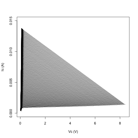
Figure 2 illustrates one of the obtained sets of indexed isolines as acquired, without any smoothing or pre-processing, which indicates a good signal to noise level. Observe the increasing slope of the isolines as goes from (bottom) to (top), which is an intrinsic characteristic of the Early effect. Next, each of these sets of isolines is slightly smoothed through an average filter (11 points wide) and resampled so as to have the same number of isolines in all cases costaearly:2017 ; costaearly:2018 .
The Hough transform-inspired voting (or accumulating) scheme used for numeric estimation of typically resulted in sharp, well-defined peaks such as that illustrated in Figure 3. Observe that only a region of the space, corresponding to where the isolines tend to intersect, needs to be considered in the Hough mapping and voting. The coordinate (-axis) of the peak is taken as the most likely value of for each transistor. Observe that the peak of isolines intersections in the space does not occur exactly on the axis, with a small offset in the order of one being obtained in the peak coordinates. The use of the Hough transform-inspired voting allows eventual isolines diverging too much from the others not to be considered.
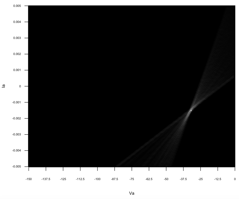
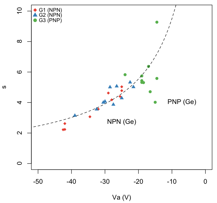
Figure 4 presents the obtained distributions of germanium NPN and PNP junction transistors in the Early space . The two NPN types, namely and resulted with very similar Early parameters, therefore exhibiting great overlap in the Early space in Figure 4. This means that these two types of NPN germanium transistors have very similar electronic properties, at least considering the adopted samples/configurations and non-reactive loads. The PNP group, identified as in this figure, resulted with distinctively higher values (smaller magnitudes), and also larger values of the proportionality parameter than the devices in the two NPN groups. The two groups have their centers of mass (averages) very near to the isoline defined for , which is shown by the dashed curve in this figure.
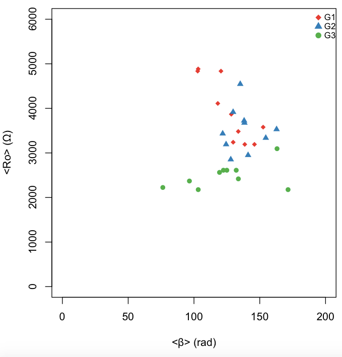
The scatterplot derived by the adopted Early methodology for the more traditional and electronically intuitive parameters and is depicted in Figure 5. As in the Early mapping, the two NPN groups largely overlap one another, and are also less separated from the PNP than in that other space. Similar levels of parameter variations are observed in this space for any of the three types of germanium transistors. In addition, the PNP devices yielded smaller values.
II.2 Comparison with Silicon BJTs
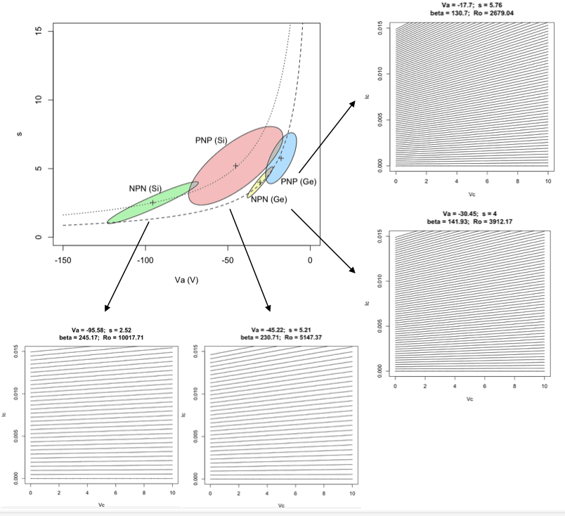
It would be particularly interesting if the electronic characteristics obtained for germanium junction transistors could be compared with those of more modern silicon bipolar junction transistors – BJTs. Fortunately, this can be done by using recently obtained results costaearly:2018 regarding the latter type of transistors. A total of 14 types of small signal BJTs (7 NPN and 7 PNP), each represented by 10 samples, were characterized in that work by using the same Early approach adopted here. Figure 6 presents the mean and dispersion (Mahalanobis ellipses johnson:2002 ) obtained for the four groups — NPN (Ge), PNP (Ge), NPN (Si) and PNP (Si) – in the Early space. Each ellipse was obtained from the respective covariance matrices by considering unit Mahalanobis distance johnson:2002 , specifying the same number of samples to comprised, in the average, inside each respective ellipse. The means of each group are marked by the “” sign. The isolines corresponding to and are also represented by the dotted and dashed lines, respectively. The prototypical characteristic surfaces respectively induced in the transistor operation space are also shown in the separated plots, providing a direct graphic representation of the typically expected electronic properties for each of the considered groups.
Several remarkable results can be inferred from Figure 6. First, we have that the NPN-PNP groups obtained for germanium look like the silicon pairs scaled so as to have smaller magnitude and slightly higher values of . Interestingly, the elongation of all groups tend to be mostly aligned with the tangent of the respective isolines at their respective centers of mass. More specifically, the germanium and silicon pairs have, in the average, respectively and . Thus, the silicon devices tend to have, in the average, twice as much current gain and smaller magnitude values, implying larger magnitudes. The average values obtained for the germanium NPN and PNP transistors were smaller than those obtained for the two silicon groups. PNP devices tended to present larger parameter variability for both germanium and silicon, but germanium transistors were – surprisingly – characterized by smaller absolute parameter variations than those observed for silicon counterparts.
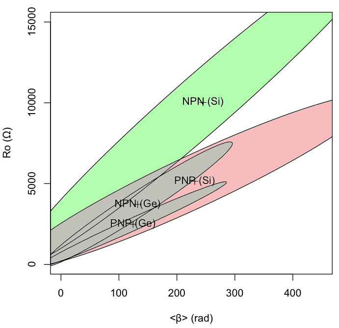
Figure 7 depicts the four transistor groups in the more traditional parameter space defined by and , also including the respective unit Mahalanobis ellipses. Unfortunately, the relative properties of the considered transistor groups can hardly be discerned in this space, as many ellipses overlap strongly. In addition, the relative features of the transistor groups, so evident in Figure 6, can hardly be inferred from this parametric representation. This striking contrast of results can be understood as corroborating the efficacy and naturality of the Early space with respect to the more traditional parametrization induced by and . The latter space, however, is underlain by more intuitive electronic interpretation, especially when analyzing/designing circuits. So, it may be interesting to consider the twin representation of transistors in the Early as well as in more traditional parametric spaces, the former being more discriminative and inherently compatible with the geometry of transistor operation and the latter being electronically more intuitive.
III Concluding Remarks
The advances of electronics since the development of the transistor have been so impressive and continuous that the critical importance that germanium devices played from the 50’s to the 60’s tends to be overlooked. The present work reported a brief excursion into the origins of modern electronics. More specifically, new old stock germanium junction transistors were characterized by a recently introduced theoretic-experimental-numerical approach based on the Early effect, as well as on image processing/analysis and pattern recognition concepts and methods. Two types of NPN and one type of PNP new old stock small signal germanium transistors were scanned electronically and the obtained signals were used to derive the respective characterization in the Early, as well as in the more traditional and electronically intuitive space.
Remarkable results were obtained with respect to both the main reported investigations, namely the characterization of germanium junction transistors and their comparison with more modern silicon BJT devices. Perhaps the principal contribution of this work is the characterization of the considered four groups of devices — NPN (Ge), PNP (Ge), NPN (Si) and PNP (Si) — in both the Early and the more traditional spaces. This characterization was performed in terms of the center of mass (average) and dispersion (Mahalanobis distance, derived from the respective covariance matrices), as well as -indexed isolines. A surprisingly well-defined distribution of the transistor types resulted in the Early space, with the NPN devices exhibiting greater parametric variation for both silicon and germanium. Yet and remarkably, unlike it is sometimes believed, the old germanium devices presented substantially smaller parameter variation than the considered modern silicon devices. The four groups of transistors also resulted remarkably separated, with little overlap between them, indicating that, at least for the adopted devices, these groups have well-defined specific characteristics. Germanium devices tended to have smaller magnitude (hence smaller ), while yielding values comparable to those of silicon devices, and was found to be about half of their silicon counterparts.
At the same time, the mapping of the four groups of transistors in the more traditional and electronically intuitive space yielded largely overlapping groups to a level that substantially undermines the identification of interesting relationships observed for the Early mapping. It is believe that, because of their complementary features, these two spaces could be used jointly while analyzing and designing devices and circuits.
It should be reminded that the reported results are specific to the devices, methods and configurations adopted in this and previous works costaearly:2018 . In particular, a limited number of new old stock alloy junction transistors were used, so that distinct results can be eventually obtained for other technologies (e.g. grown junction) and even for other models of alloy junction devices. Additional research is needed to complement the characterization under other circumstances and for additional device types. In addition, it is important to bear in mind that the reported results were derived from new old stock devices from the 50’s and 60’s, so that it becomes difficult to identify if the obtained characteristics derive from germanium material itself or from the fabrication methods and technology used in the 50’s and 60’s. It remains an interesting question to verify how modern junction germanium transistors would compare to the here obtained results for new old stock. It would also be worth investigating further the influences of the features observed for the considered devices in typical circuit applications, including the determination of gains, input and output resistances, distortion, and other properties. Of particular interest would be to perform AC analysis of the devices and circuits, as the present work was limited to DC estimation of the transistor features, as it is known that reactive components of transistors can strongly influence AC circuit operation. Yet, the features obtained for the considered new old stock germanium transistors are interesting themselves, especially in the sense that they tend to populate areas of the Early space not well covered by silicon devices, therefore providing valuable design alternatives regarding distinct and features. As a matter of fact, it would be of great potential value to have prototypes of additional devices (such as optocoupler, high frequency and high power transistors, MOSFET, silicon-germanium heterojunction, Darlington, etc.) incorporated into the obtained Early space, so as to achieve a kind of general atlas that could be used to assist electronic analysis and design. A possible reason why such maps have not become widely available is the fact that the parametric mapping of devices into more traditional spaces, as hinted by the here considered and reported cases, tend to imply larger overlap between the groups. The neat separation obtained in the Early space seems to substantiates this approach as providing a more natural and inherently effective means for mapping and studying junction transistors, as well as other similar devices.
Acknowledgments.
Luciano da F. Costa thanks CNPq (grant no. 307333/2013-2) for sponsorship. This work has been supported also by FAPESP grants 11/50761-2 and 2015/22308-2.
References
- (1) L. da F. Costa. Characterizing complementary bipolar junction transistors by Early modelling, image analysis, and pattern recognition, 2018. arXiv preprint arXiv:1801.06025v2.
- (2) L. da F. Costa, F. N. Silva, and C. H. Comin. Negative feedback, linearity and parameter invariance in linear electronics. Electrical Engineering, (3):1139, 2017.
- (3) L. da F. Costa, F.N. Silva, and C.H. Comin. An Early model of transistors and circuits, 2017. arXiv preprint arXiv:1701.02269v2.
- (4) R. C. Jaeger and T. N. Blalock. Microelectronic Circuit Design. McGraw-Hill New York, 1997.
- (5) R. A. Johnson and D.W. Wichern. Applied multivariate statistical analysis. Prentice Hall, 2002.
- (6) M. H. Jones. A Practical Introduction to Electronic Circuits. Cambridge University Press, 1969.
- (7) Boylestad R. L and L. Nashelsky. Electronic Devices and Circuit Theory. Pearson, 2008.
- (8) G Parker. Introductory Semiconductor Device Physics. Taylor & Francis, 2004.
- (9) M. Riordan and L. Hoddeson. Crystal Fire – The Birth of the Information Age. W. W. Norton & Co., 1997.
- (10) A. Sedra and K. Carless Smith. Microelectronic circuits. Oxford University Press, New York, 1998.
- (11) J. L. Stewart. Circuit Theory and Design. John Wiley & Sons, 1956.
- (12) S. M. Sze. Circuit Theory and Design. Wiley-Interscience, 1969.