Twelve Inequivalent Dirac Cones in Two-Dimensional ZrB2
Abstract
Theoretical evidence of the existence of 12 inequivalent Dirac cones at the vicinity of the Fermi energy in monolayered ZrB2 is presented. Two-dimensional ZrB2 is a mechanically stable d- and p-orbital compound exhibiting a unique electronic structure with two Dirac cones out of high-symmetry points in the irreducible Brillouin zone with a small electron-pocket compensation. First-principles calculations demonstrate that while one of the cones is insensitive to lattice expansion, the second cone vanishes for small perturbation of the vertical Zr position. Internal symmetry breaking with external physical stimuli, along with the relativistic effect of SOC, is able to remove selectively the Dirac cones. A rational explanation in terms of d- and p-orbital mixing is provided to elucidate the origin of the infrequent amount of Dirac cones in a flat structure. The versatility of transition metal d-orbitals combined with the honeycomb lattice provided by the B atoms yields novel features never observed in a two-dimensional material.
I Introduction
In the search of the materials of tomorrow’s technology, graphene was considered early on as a promising candidate for development and innovationNovoselov et al. (2004). The combination of an electronic band structure hosting the so-called massless Dirac fermions, together with a weak spin-orbit coupling (SOC), enable electrons to travel at relativistic speed over very long distances at room temperature. Governed by the Dirac equation, Dirac fermions emerge at isolated points in the irreducible Brillouin zone (iBZ), where an upper band touches a lower one. In undoped graphene, two Dirac cones are centered around the two non-equivalent K and K’ points with a perfect electron-hole symmetry at the Fermi level. Each Dirac cone is therefore three-fold degenerate since they are shared by three contiguous BZ, namely a BZ contains the equivalent to two inequivalent cones.
Experimental results confirmed the ability of other two-dimensional (2D) group IV materials (siliceneVogt et al. (2012); Grazianetti et al. (2016), germaneneDávila et al. (2014); Acun et al. (2015), staneneZhu et al. (2015)) for hosting Dirac states, and theoretical predictions suggested new compounds with similar properties (graphynesMalko et al. (2012), 8-pmmn boropheneLopez-Bezanilla and Littlewood (2016)). In most cases, 2D honeycombed lattices with Dirac cones are composed of a single type of element. Although binary compositions usually yield gapped electronic structures (BNKim et al. (2012), MoS2Mak et al. (2010)), branching away from the single-element material and search for multi-atom compounds may yield similar benefits.
More recently, the fabrication of a diverse array of 2D B monolayers has captivated a growing community of scientific experts focusing on their large list of exceptional physical propertiesMannix et al. (2015); Feng et al. (2016). B-based materials with additional electron-rich elements are potential candidates to expand the number of compounds with similar properties to the group IV materials. The discovery of high Tc superconductivity in MgB2 Nagamatsu et al. (2001) caused an immediate interest to find B-based superconductors. The viability of this compound, similar to other planar diboridesHall and Compton (1965) such as B2O and B2Be, relies in that it is unsymmetrical isoelectronic to C, with four valence electrons per atom in average. 2D B-monolayers incorporating elements with larger principal quantum numbers may benefit of the richness of d orbitals. Thus, first-principles calculations predicted the existence of massless fermions in monolayered TiB2 Zhang et al. (2014). Polymers containing both boron and transition metals atoms have been prepared, proving a high degree of delocalization via boron and metal atomsMatsumi et al. (2001).
In this paper the potential scope of diborides is expanded by describing the electronic properties of metal diboride monolayered ZrB2. Free-standing ZrB2 is triangular borophene with Zr atoms in substitutional doping, and is predicted to exhibit 12 non-degenerate Dirac cones in the vicinity of Fermi level with a small compensated electron-hole pocket. This material features an infrequent property in a hexagonal lattice such as the displacement of the Dirac cones to lines joining two high-symmetry points of the iBZ. Both hexagonal -graphyneMalko et al. (2012) and TiB2Zhang et al. (2014) have been reported to exhibit six low symmetry Dirac points in the first BZ, and the use of Rashba SOC has been proposedvan Miert and Smith (2016) for splitting them into 12. Instead of resorting to the spin degree of freedom, we propose the interplay of p and d orbitals to generate six groups of two inequivalent Dirac cones in the low energy spectrum of a P6mm space group material. Zr atom d-orbitals yield the formation of the Dirac cones with some contribution from the B pz orbitals. For the sake of clarity, it must be noted that the 12 cones refer to both the 12 upper and 12 lower cones that in pairs are created in the vicinity of the Fermi level.
Contrary to the current trend of identifying new materials with improved functionalities by means of high-throughput screening of thousands of compounds, here we present a one-at-a-time material study to provide a detailed analysis of a nanostructure designed upon examination of the physico-chemical properties of its constituents.
II Computational Methods
Calculations were performed with the SIESTA code. A double- polarized basis set was used and the radial extension of the orbitals had a finite range with a kinetic energy cutoff of 50 meV. Electron exchange and correlation was described within the Perdew, Burke, and Ernzerhof Kresse and Furthmüller (1996) scheme of the generalized gradient approximation. The integration in the k-space was performed using a 32321 Monkhorst-Pack Monkhorst and Pack (1976) k-point mesh centered at -point. To determine accurately the location of the Fermi level, a set of 3203201 k-points were used in a single-energy point calculation. Lattice constants and atomic coordinates were fully relaxed until the residual forces were smaller than 10-3 eV/Å. Phonon diagram dispersion was calculated with the PHONOPY code Togo and Tanaka (2015) using the force-constant method, and the dynamical matrices were computed using the finite differences method in large supercells. Single-energy point SOC calculations were carried out with Elk codeElk with similar effective parameters.
III Results and Discussion
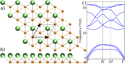
In 2D ZrB2, the honeycomb lattice of B atoms exhibits a B-B distance of 1.85Å, and the Zr atoms sit over the hexagon hole at 1.48Å (see Figure 1a and b). The lattice parameter is 3.17Å. With its vacant pz orbital, three-fold coordinated B is an electron deficient atom and a strong p-electron acceptor.
Before inspecting the electronic properties of the free-standing ZrB2 monolayer, it is worth analyzing their origin from the bulk configuration. Vertical AA stacking of single hexagonal layers yields bulk ZrB2, a ceramic material with a hexagonal covalent structure possessing good thermal and electrical conductivities. The crystal structure belongs to the space group P6/mmm, where the Zr atoms sit in between two hexagons of two B honeycombed network. Temperature dependent resistivity and high frequency susceptibility measurements in ZrB2 revealed a superconducting transition at 5.5 KGasparov et al. (2001). Thin films of ZrB2 can be grown by chemical vapour epitaxy on Si wafers, to additionally provide an electrically conductive substrate for GaNKinoshita et al. (2001), or the synthesis of monolayered materials Gill et al. (2017).
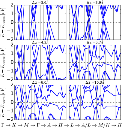
The series of electronic band diagrams in Figure 2 shows the evolution of the electronic states of ZrB2, from bulk to monolayer, with successive increases of the distance between stuck layers with no geometric optimization of the atomic positions. The origin of the good bulk conducting properties are clearly explained by the numerous metallic bands, including some band-crossing forming Dirac cones at the vicinity of the Fermi level, such in the line and lines. For a small increase of Å, a first gap appears in the line at 0.4 eV, while in the vicinity of the point new lines cross the Fermi level and a Dirac cones is defined. This cone lowers in energy at Å, and backs up at Å while the cone in the line vanishes. At a Å interlayer separation only four metallic bands remain, and for Å the Dirac cones defining the properties of monolayered ZrB2 are finally defined.
Isolating a single layer reduces the symmetry to P6/mm, and the BZ of interest is the area delimited by the , , and points in the hexagonal reciprocal lattice. The monolayer is dynamically stable as verified by the absence of negative frequencies in the phonon spectrum shown in Figure 1c. Only one of the acoustic modes undergoes a tiny deviation towards negative frequencies close to the point. 9 modes are extended over a frequency range of 21 THz. The in-plane acoustic branches are characterized by linear dispersions at low momentum near the center of the BZ. The out-of-plane phonon branches exhibit non-linear energy dispersions at the zone edge. While most acoustic modes exhibit 6 eV dispersive branches in the lower quarter of the spectrum, a frequency gap separates optical modes in the upper half, which are equally dispersive spanning altogether a range of 10 THz.
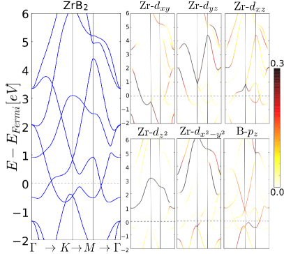
The band structure of the hexagonal 2D lattice is displayed in the left panel of Figure 3. Two bands form a Dirac cone in the line slightly above the Fermi level creating a small electron pocket. To compensate the lack of electrons, a similar hole pocket is formed upon two bands creating a second Dirac cone slightly below the Fermi energy level in the line.
In the hexagonal pyramid configuration, monolayered ZrB2 belong to the C6v point group. According to this symmetry representation, the five Zr d-orbitals are grouped in three groups, where two in-plane orbitals are degenerate (e2), two out-of-plane orbitals also form a degenerate pair (e1), and d remains non-degenerate (a1). To corroborate this picture and elucidate the origin of each Dirac cone, we resort to color-resolved projected density of state (PDoS) diagrams, which allow to visualize the independent contribution of each atomic orbital to the electronic states. At point two band-crossing occur with a difference in energy of 1.29 eV. In the valence band, the dxy and the d orbitals intersect in a two-fold degenerate point (e2), while a Dirac cone at 0.87 eV in the conduction band is created upon the dyz and the dxz Zr orbitals meet in a degenerate pair (e1). The d orbital stands alone at 3.13 eV (a1). Note that the intensity of the lines depends on the contribution but also on the normalization factor and, although some states may appear weakly represented, the presence with light colors at the Fermi level guarantees their contribution to the Dirac cones.
The PDoS show evidence that the Dirac cone at the Fermi energy is created predominantly by the combination of Zr d-orbitals, whereas in the cone B pz orbitals have a greater contribution. The former derives from the dxy, dxz, and dyz orbitals, while the latter is mainly composed of dxz and dyz states hybridized with the B atom pz orbital. A reminiscence of the boron honeycomb lattice is evident in the contribution of the B pz orbitals to the Dirac cone at the point located at 0.9 eV, in whose formation the dyz for the upper cone and the dxz for the lower one also participate. The two d and d orbitals form anti-bonding states at high energy levels and do not contribute in any case to the formation of any Dirac cone. However, and as discussed below in more detail, although B atoms are crucial in the formation of the Dirac points, each cone presents different sensitivity to hybridization changes.
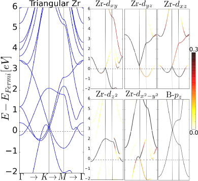
To further support this picture of d- and p-hybridized derived Dirac states, the band diagram of the triangular lattice formed uniquely by Zr atoms at fixed positions, and with all B atoms removed, is plotted in Figure 4. A single panel showing the band developed by the lateral superposition of B atom pz orbitals with no Zr atoms sitting on the hexagons is included. Interestingly, bands are shifted in energy and conserve the main features of the complete lattice, except the Dirac cones at the high-symmetry lines. The same group of four bands crossing at the point are distinguishable although within a much reduced energy range of 0.16 eV. In the line, the band intersection observed at 0.17 eV is composed of the dxz orbital for the running up band, and of the dxy and d orbitals at the bending region of the running low band. Upon introducing the B atoms, pz orbitals mix with low-energy d orbitals in this region of the BZ and allow the formation of the Dirac cone. Similarly, in the first half of the line, there is no running up band that may yield the Dirac cone observed in the diborade lattice, other than the d derived band which is known from the diboride diagram to not mix with any other state. Furthermore, the dxz state is developed from 0.43 eV down to -0.37 eV across that region, contrary to the observation in Figure 3, where it is developed from to with positive gradient. Such a change in the slope of the band can be ascribed to the presence of the B atom pz orbitals when they enter the formation of the diboride lattice, which also causes the d and d orbital derived bands to shift up in energy. This proves that the Zr-B orbitals interplay is crucial in the formation and strength of both Dirac cones, allowing the Zr-B hybridization to locate both Dirac points in the vicinity of the Fermi level, and the electronic delocalization over the complete unit cell.
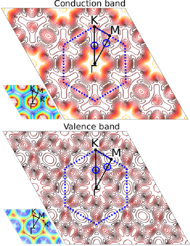
Applying the symmetry operations of the C6v point group to the iBZ, two dimensional ZrB2 exhibits 12 inequivalent Dirac cones, which is a remarkable difference with respect to any previously described hexagonal material. This is displayed in the contour line plots of both the valence and conduction band shown in Figure 5, where the same bands of graphene have been included for comparison. Indeed, rotating the iBZ six times to complete the whole BZ of the hexagonal lattice (pointed out by the dashed hexagons), six groups of two Dirac points are reproduced. Note that applying the same operations on the graphene BZ yields three groups of a pair of K and K’ points hosting the corresponding cones.
Due to the large size of the Zr atom, SOC is susceptible to introduce some changes in the electronic states. SOC was checked and the resulting band diagram is shown in Figure 6b. meV large band gaps are noticeable at all band crossing, while the rest of the electronic states barely differs from the non-relativistic band structure. It is worth noting that electron-hole pockets are preserved and the band splitting causes a distortion of the Dirac cone in the line that closes effectively an, in principle, small gap by overlapping the bands, as shown in detail in the zoom-in inset.
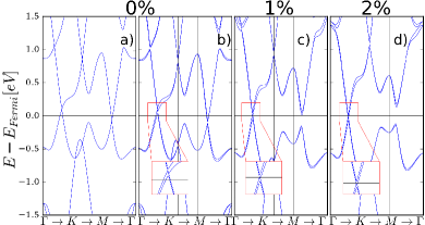
Despite both types of Dirac cones derive from the Zr d-orbitals, the stronger hybridization with the B atoms exhibited by the cone on the line makes it very sensitive to relative distance variations. External tensile strain expands the lattice and the Zr atom adjusts its vertical distance to the honeycomb lattice, and is able to vanish the Dirac point. Figure 6 shows the evolution of the ZrB2 electronic states with SOC under increasing tensile strain up to 2%. The vertical distance to the center of the hexagon is progressively reduced from the original 1.48Å down to 1.44, 1.41, 1.37, and 1.33Å for an enlargement of the hexagonal unit vectors from 1% to 2%, 3% , and 4% respectively. Although the hexagons expand, providing more room to accommodate the Zr atom, the Zr-B bond length is barely modified. The main effect leading to the Dirac cone vanishing can be ascribed to the difference in the pz - d orbital hybridization as a result of the bonding angle modification. These structural changes, that leave the triangular geometry of the Zr atom intact, preserve the Zr-derived Dirac cone in the line. Although the cone is created with the participation of the B atoms that turn over the slope of the dxz derived band, it is less sensitive to hybridization effects. With no other metallic band to compensate the hole pocket, the Dirac point shifts to exactly the Fermi energy. Similarly, the cones at the point are separated by a slightly larger gap.
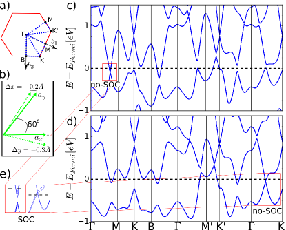
A distinctive feature of graphene low-energy spectrum is that the Dirac cones at and ’ points are protected by symmetry and from any perturbation that does not violate parity and time reversal symmetries. The metallic character of graphene electronic structure is thus insensitive to deformations such as external stress. On the contrary, the hexagonal network of ZrB2 is highly sensitive to shear stress which reduces the symmetry of the unit cell and causes the vanishing of either the or Dirac points, depending on the direction of the external force. Figure 7a displays the shape of the BZ after symmetry reduction. The modification of the unit cell is realized by modifying one unit cell vector component at a time, as shown in Figure 7b, where the angle between in-plane unit cell vectors is increased. Figure 7c shows the electronic band diagram of ZrB2 obtained upon applying an external force acting parallel to the x-axis that subtract 0.2 Å to the x-component of the unit cell vector. Dirac cones in the -M line split due to the SOC (see inset) and are preserved despite the symmetry reduction, while the Dirac point in the line vanishes. Band degeneracy at the and points is also removed. Similarly, decreasing by 0.3 Å the y-component of the vector, a force acting along the y-axis is mimicked. As a result, only the Dirac cone in the line remains unaffected.
IV Conclusions
The existence of twelve inequivalent Dirac cones in the low spectrum diagram of a hexagonal lattice can be realized, without resorting to Rashba SOC or twisted bilayer of triangular latticesvan Miert and Smith (2016). Owing to the formation of monolayered ZrB2 Dirac cones in the lines joining high symmetry points, the cones are not shared with any neighbouring BZ. The twelve Dirac cones are divided in six groups of two non-symmetry-related cones with a slight electron-pocket compensation. First-principles calculations allowed to unveil the separate contribution of each d-orbital of the transition metal atom, and their hybridization with the B atomic orbitals. A color-scheme enabled to assign the formation of the cones to the Zr dxy, dxz, and dyz orbitals with a contribution from B pz orbitals as a result of atomic orbital hybridization.
Dirac cones are modified under external physical stimuli differently as a result of the unidentical participation of the B pz orbitals in the formation of the cones. Owing to the strong Zr-B atoms hybridization, small perturbations in the bonding angle lead to one cone vanishing. Ignoring SOC, internal symmetry breaking leads to a selective Dirac cone disruption at Fermi level depending on the direction of applied distortion, showing that not all cones are protected by symmetry. SOC induces complete Dirac point vanishing depending on the direction of the external force. These findings suggest that the interplay between d and p orbitals of different atoms, together with the relativistic effect of SOC, creates an environment that offers new avenues to electronics, and may provide a platform that outdoes the capabilities of other 2D materials with Dirac states.
It is worth mentioning that one key issue of monolayered ZrB2 with a view to its implementation in electronic applications is the robustness of the electronic properties against the disorder introduced by intrinsic or extrinsic defects, such as atomic vacancies and external functional groups. Both short and long range disorder are known to limit the charge transport ability of 2D compoundsRoche et al. (2012) and, therefore, a systematic analysis of the possible role of defects in an energy-dependent charge mobility framework is proposed for future studies. From our results, where minute network deformations were shown to lead inevitably to drastic changes, the electronic properties of monolayered ZrB2 can be anticipated as extremely sensitive to network changes. Thus, sensor applications by monitoring electrical changes in the nano-structure upon interaction with foreign species could be expected as a potential technological use of the material. Advanced approaches accounting for the strongly correlated Zr electrons must be considered to study the formation of localized magnetic moments upon composition changes.
V Acknowledgments
This work was supported by the U.S. Department of Energy, Office of Science, Basic Energy Sciences, Materials Science and Engineering Division. I acknowledge the computing resources provided on Blues and Bebop, the high-performance computing clusters operated by the Laboratory Computing Resource Center at Argonne National Laboratory. I thank P.B. Littlewood for fruitful discussions and support.
References
- Novoselov et al. (2004) K. S. Novoselov, A. K. Geim, S. V. Morozov, D. Jiang, Y. Zhang, S. V. Dubonos, I. V. Grigorieva, and A. A. Firsov, Science 306, 666 (2004), http://science.sciencemag.org/content/306/5696/666.full.pdf .
- Vogt et al. (2012) P. Vogt, P. De Padova, C. Quaresima, J. Avila, E. Frantzeskakis, M. C. Asensio, A. Resta, B. Ealet, and G. Le Lay, Phys. Rev. Lett. 108, 155501 (2012).
- Grazianetti et al. (2016) C. Grazianetti, E. Cinquanta, and A. Molle, 2D Materials 3, 012001 (2016).
- Dávila et al. (2014) M. E. Dávila, L. Xian, S. Cahangirov, A. Rubio, and G. L. Lay, New Journal of Physics 16, 095002 (2014).
- Acun et al. (2015) A. Acun, L. Zhang, P. Bampoulis, M. Farmanbar, A. van Houselt, A. N. Rudenko, M. Lingenfelder, G. Brocks, B. Poelsema, M. I. Katsnelson, and H. J. W. Zandvliet, Journal of Physics: Condensed Matter 27, 443002 (2015).
- Zhu et al. (2015) F.-f. Zhu, W.-j. Chen, Y. Xu, C.-l. Gao, D.-d. Guan, C.-h. Liu, D. Qian, S.-C. Zhang, and J.-f. Jia, NATURE MATERIALS 14, 1020+ (2015).
- Malko et al. (2012) D. Malko, C. Neiss, F. Viñes, and A. Görling, Phys. Rev. Lett. 108, 086804 (2012).
- Lopez-Bezanilla and Littlewood (2016) A. Lopez-Bezanilla and P. B. Littlewood, Phys. Rev. B 93, 241405 (2016).
- Kim et al. (2012) K. K. Kim, A. Hsu, X. Jia, S. M. Kim, Y. Shi, M. Dresselhaus, T. Palacios, and J. Kong, ACS Nano 6, 8583 (2012), pMID: 22970651, http://dx.doi.org/10.1021/nn301675f .
- Mak et al. (2010) K. F. Mak, C. Lee, J. Hone, J. Shan, and T. F. Heinz, Phys. Rev. Lett. 105, 136805 (2010).
- Mannix et al. (2015) A. J. Mannix, X.-F. Zhou, B. Kiraly, J. D. Wood, D. Alducin, B. D. Myers, X. Liu, B. L. Fisher, U. Santiago, J. R. Guest, M. J. Yacaman, A. Ponce, A. R. Oganov, M. C. Hersam, and N. P. Guisinger, Science 350, 1513 (2015), http://science.sciencemag.org/content/350/6267/1513.full.pdf .
- Feng et al. (2016) B. Feng, J. Zhang, Q. Zhong, W. Li, S. Li, H. Li, P. Cheng, S. Meng, L. Chen, and K. Wu, Nat Chem 8, 563 (2016).
- Nagamatsu et al. (2001) J. Nagamatsu, N. Nakagawa, T. Muranaka, Y. Zenitani, and J. Akimitsu, NATURE 410, 63 (2001).
- Hall and Compton (1965) H. T. Hall and L. A. Compton, Inorganic Chemistry 4, 1213 (1965), http://dx.doi.org/10.1021/ic50030a027 .
- Zhang et al. (2014) L. Z. Zhang, Z. F. Wang, S. X. Du, H.-J. Gao, and F. Liu, Phys. Rev. B 90, 161402 (2014).
- Matsumi et al. (2001) N. Matsumi, Y. Chujo, O. Lavastre, and P. H. Dixneuf, Organometallics 20, 2425 (2001), http://dx.doi.org/10.1021/om010258d .
- van Miert and Smith (2016) G. van Miert and C. M. Smith, Phys. Rev. B 93, 035401 (2016).
- Kresse and Furthmüller (1996) G. Kresse and J. Furthmüller, Phys. Rev. B 54, 11169 (1996).
- Monkhorst and Pack (1976) H. J. Monkhorst and J. D. Pack, Phys. Rev. B 13, 5188 (1976).
- Togo and Tanaka (2015) A. Togo and I. Tanaka, Scr. Mater. 108, 1 (2015).
- (21) Elk is an all-electron full-potential linearized augmented plane wave with local orbitals [FP-(L) APW+lo] code, available free of charge at http://elk.sourceforge.net.
- Gasparov et al. (2001) V. A. Gasparov, N. S. Sidorov, I. I. Zver’kova, and M. P. Kulakov, Journal of Experimental and Theoretical Physics Letters 73, 532 (2001).
- Kinoshita et al. (2001) H. Kinoshita, S. Otani, S. Kamiyama, H. Amano, I. Akasaki, J. Suda, and H. Matsunami, Japanese Journal of Applied Physics 40, L1280 (2001).
- Gill et al. (2017) T. G. Gill, A. Fleurence, B. Warner, H. Prüser, R. Friedlein, J. T. Sadowski, C. F. Hirjibehedin, and Y. Yamada-Takamura, 2D Materials 4, 021015 (2017).
- Roche et al. (2012) S. Roche, N. Leconte, F. Ortmann, A. Lherbier, D. Soriano, and J.-C. Charlier, Solid State Communications 152, 1404 (2012), exploring Graphene, Recent Research Advances.
1